Design of Automatic Timing Verification Tool for FPGA Systems
Abstract
Speeding up verification is a significant issue on development of FPGA systems. During pre-simulation phase, the simulator only generates stimulus and response with behavior of circuits. However, simulation and debugging steps in designing a complex system require extremely long and time-consuming test sequences. In this work, we propose an efficient verification method to automatically verify between golden data and simulation results on bus transaction in FPGA systems.
Additionally, we also develop and integrate an enhanced FPGA verification tool with graphic user interface to verify user’s design. Finally, a simple CPU design example will be demonstrated to show the feasibility of proposed tool.
Keyword: FPGA system, Bus transaction, Timing verification
1. Introduction
Nowadays, with millions of gate counts design is often development in consumer electronics. While considering cost-down issue of verification, FPGA is the cheapest prototyping platform to combine design to stimulus. However, some verification tools are provided by CAD/EDA companies FPGA vendors for system design. But some verification issues are still lack the valid method to solve such as time consuming, exploded transitions and enormous test patterns.
ModelSim 6.1f software is a well-known simulation tool that is developed by Mentor Graphics.
After Xilinx ISE synthesizes VHDL or Verilog design, designer can further edit testbench waveform file by Xilinx ISE by for behavioral simulation. The other tool known as ChipScope Pro software is so called
“software logic analyzer”. It makes verification of FPGA platform analyzable and investigable by JTAG interface which defined IEEE 1149.1 standard and communicates status with external/internal signals.
According to ChipScope Pro design flow, designer can firstly use ChipScope Pro core inserter to set
probe points on external/internal signals. Next, both design and set probe points will be synthesized, placed and routed in order by Xilinx ISE. Finally, designer downloads the executing program of bit stream into FPGA and observes waveforms of probe signals.
For complex system design, designers often use module-based design. A complex system design is partitioned into several modules. These modules are IPs or custom designs with correct functionality.
However, a complex system design may work abnormally due to bus transaction errors between modules. To find bugs, designer often observes timing diagram in simulator to debug. The debugging will cost much time and effort. Testbench only records stimulus and response. Analysis between testbench and golden data is an artificial task. Such task may not find out bugs due to carelessness. Therefore, verification of bus transaction has been studied due to the practical importance in the FPGA system design.
In this work, we propose an algorithm and develop a verification tool that automatically detects the differences between golden data and testbench of simulation result.
The remainder of this paper is organized as follows. Section 2 presents preliminaries of this paper.
In Section 3, we propose a method to solve the verification for bus transaction. In Section 4, we present the design of user graphic interface.
Experimental results are shown in Section 5. Finally, the conclusion is given in Section 6.
2. Preliminaries
Advanced fabrication process technology drives the capacity of FPGA to hundred of millions logic elements or more. Verification in FPGA of high capacity must be a time-consuming and hard work. In 2001, Rashinkar et al. [1] estimate the cost of verification in 40% to 70%. In order to reduce efforts and time-consuming, some researchers have been investigated on verification of FPGA in recent years.
With fast hardware/software co-verification, Nakamura et al. [2] propose the simulation of hardware/software interface which used sharing communication register (SCR) as a bridge between Trong-Yen Lee1, Chou-Chuan Yao1, Yang-Hsin Fan1,2, Chia-Chun Tsai3, Rong-Shue Hsiao1
1Dept.of Electronic Engineering and Institute of Computer and Communication Engineering, National Taipei University of Technology, Taipei, Taiwan, R.O.C.
2Information System Division of Library, National Taitung University, Taitung, Taiwan, R.O.C.
3Dept. of Computer Science and Information Engineering, Nanhua University, Chia-Yi, Taiwan, R.O.C.
1{tylee, t5418069, rshsiao}@ntut.edu.tw, 2yhfan@nttu.edu.tw, 3chun@mail.nhu.edu.tw
simulator and emulator. Moreover, peripheral component interconnect (PCI) local bus is also used to communicate with simulator and emulator in their research. Lin et al. [3] also design dynamic and static monitoring methods to modify embedded software even the system is running. In 2004, Chuang et al. [4]
use “snapshot” method to record status of internal registers of a FPGA. Next, they replay the signals in a software simulator to debug. For emulating issue, Oh et al. [5] use four Xilinx Virtex-1000 FPGAs to combine an emulator for functional verification of multi-media processor. They also insert debugging module for trap debugging in each FPGA. For their propose method, the emulator provides virtual wires to overcome the problem, but even physical wires are not enough. In bus transaction verification, Huang et al. [6] propose language-based methodology to generate transaction extractors for on-chip buses.
They state that their approach can reduce verification time of internal interfaces between IPs.
In our previous work, we have developed a tool, namely FVT (Functional Verification Tool) [7], to automatically verify among the user definition specification file, output testbench waveform file and testing waveform file which is generated by ModelSim and Xilinx ChipScope Pro, respectively.
3. Verification Method for Bus Transaction
Normally, a timing diagram is used for debugging in a system design. However, designer spends much effort to check between the golden data and testbench.
Designer may make mistakes while checking between the golden data and testbench. This work proposes a method to compare golden data and testbench for bus transaction automatically. Therefore, proposed method reduces mistakes due to carelessness and speeds up verification time of bus transaction for FPGA systems.
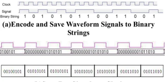
Control signal such as write signal waveform can be encoded and saved as binary string per clock.
Figure 1(a) illustrates an example that waveform is encoded to binary string as 101010110011001. Unlike control signal, bus signal can be saved multi bits per clock such as Fig. 1(b). Therefore, we save control and bus signal into arrays and perform verification algorithm for bus transaction.
If control signal is input, proposed method compares the first digit and the 8th in golden data and testbench. If the result is true, hush function from the first digit to 8th digit will be calculated. Hash values of testbench and golden data are compared. If they are equal, other digits between the golden data and testbench will be compared. Next, golden data will be shift right 1 bit and repeat above process. Fig. 2(a) shows the detail process for our proposed method.
Figure 2(b) shows detail verification process for bus signal. Golden data are compared with corresponding testbench and then the comparison of results will be output.
(a)Encode and Save Waveform Signals to Binary Strings
(b)Save Bus Signal per Clock
Fig. 1 Saving Format for Two Types of Signals
… Testbench
Golden Data, hash value=p
1 0 1 1 1 1
1 1 1 1 1
0 0
0 0 0
1 0 1 0 1 0 1 1
(hash value of testbench = q)
… Testbench
q
(hash value of golden data=p)
q = p ?
true
1 1 1 1 1
0 0
0 0
0 0 0 0 0
true
… Testbench equal? equal?
equal?
1 0 1 0 1 0 1 1 Golden Data
… Testbench
1 1 1 1 1
1 1 1 1
0 0 0 0 0
0 0 0 0
equal? equal?
Golden Data true, output answer and shift right 1 bit
repeat above process
false
false false
Shift right 1 bit
(simulation result)
(simulation result)
(a) Process of Control Signal Verification
00100101
00100101 01010101
01010101 01010101
01010101 10101010
10101010 10101010
10101010 01011010
01011010 01011010
01011010
… Testbench
Golden Data output answer and golden data shift right 1 bit
… Testbench equal?
00100101 01010101 01010101101010101010101001011010 01011010
00100101 01010101 01010101 10101010 10101010 10101010 10101010 equal?
Golden Data (simulation result)
(simulation result)
(b) Process of Bus Signal Verification Fig. 2 Process of Verification Method
TABLE I Bus Verification Algorithm
Table I shows the verification algorithm for bus transaction that consists of 11 steps. If we verify control signals such as write signal, step 3 will be performed. Hash value of golden data is calculated by hash function. In step 4, the first digit of golden data and ith digit of testbench will be compred. The mth digit of golden data and the [i+m-1]th comparison will also be performed in this step. Both of above answers are true, hash value of testbench from i to i+m-1 will be calculated in step 5. In step 6 and 7, if hash value of golden data pattern equals current testbench, other digits between golden data pattern and current testbench will be compared. Step 8 may not be run if the result of step 7 is false. Step 4 to 8 will be performed repeatedly until for loop running completely.
If we verify bus signals such as address bus, step 10 will be performed. Step 10 compares golden data and testbench. Step 11 may not be run if the result of step 10 is false. Step 10 to 11 will be performed repeatedly until for loop running completely.
4. User Graphic Interface Design
We not only present verification method for bus transaction but also design a friendly graphical user interface (GUI) for designer. Fig. 3 shows the GUI which is used to verify the design between user given golden data and testbench. The GUI and verification algorithm are integrated in a tool, namely EFVT (Enhanced FPGA Verification Tool) for verification of FPGA system. EFVT is developed under Microsoft
Fig. 3 The Integrated Verification Tool: EFVT
Fig. 4 Process Flow of EFVT Visual Basic 6.0.
Figure 4 shows the process flow of EFVT.
Testbench file is generated by ModelSim and the golden data is produced by C, C++ or designer definition. Testbench reader and golden data reader not only reads testbench file and golden data, respectively but also builds data in memory. Next, testbench and golden data is inputted to BUS verification algorithm separately. Finally, program outputs verification results that include timing information and pattern occurring position in testbench.
Testbench reader builds data according to information such as signal name and timing record listed on testbench file. Functionality of golden data reader is the same as testbench reader. Nevertheless, format of golden data file is different from testbench file. Interpretation method between golden data reader and testbench reader are different.
5. Experimental Results
For demonstration our proposed tool, we design and implement a simple CPU design example that includes an ALU, buses and memory as shown in Fig.
5. ALU computes data and store result into memory.
Besides, we add function of bus control into ALU;
therefore the role of ALU is also a bus controller. This ALU operates adding, subtraction, multiplying and Verification Algorithm for Bus Transaction
(testbench[1..n],golden_data[1..m]) 1 Select Case;
2 Case: Control Signal
3 h_golden_data=hash(golden_data[1..m]) for(i=1; i<=n-m+1; i++)
{
4 if (testbench[i]=golden_data[1]) and (testbench[i+m-1]=goden_data[m]) then 5 h_testbench=hash(testbench[i..i+m-1]) 6 if h_golden_data=h_testbench then 7 if testbench[i+1..i+m-2]=
golden_data[2..m-1] then 8 print “occurs on” i “to” i+m-1 end if;
end if;
end if;
}
9 Case: Bus Signal for(i=1; i<=n; i++) {
10 if testbench[i..i+m-1]=
golden_data[1..m] then 11 print “occurs on” i “to” i+m-1 end if;
} End Case;
End Select;
Output verification results
input Golden Data input Testbench
EFVT
Testbench file generated by ModelSim
Golden Data produced by designer
Golden Data reader Testbench reader
Running BUS verification algorithm
TABLE II Operation of Instruction Code Instruction Code Operation
000 Adding 001 Subtraction 010 Multiplying 011 XOR 100 AND 101 OR 110 Write data to result memory
111 Move data from source memory A to result memory
ALU/BUS Controller
Instruction Memory
Source Memory A
Source Memory B
Result Memory Instruction bus
3
8 8
16 Data Bus A Data Bus B
Result Data Bus
Fig. 5 A Simple CPU Architecture
logical functions such as AND, OR, XOR and data moving. Two input data buses and one output result data bus are 8 bits and 16 bits, respectively.
Instruction bus and data buses are isolated. ALU runs program sequentially and not support jump instruction.
ALU also fetches operands sequentially.
There are four memories in the system, such as instruction memory, source memory A, source memory B and result memory. Instruction memory stores instructions such as adding, subtraction, multiplying, AND, OR and data moving. Source memory stores operands and test patterns. Once ALU operates data moving instruction, data will move from source memory to result memory. Result memory also stores arithmetic and logical operation results.
Instruction codes are listed summary as Table II.
The environment of experiments includes personal computer (PC), Xilinx ISE 8.2i, and ModelSim SE 6.1f. The PC is running on Pentium IV 2.8GHz with HT (hyper-threading technology) and 1GB RAM. We design and implement the simple CPU by VHDL and synthesis tool by Xilinx ISE 8.2i. Testbench file and golden data file is generated by ModelSim 6.1f and designer, respectively.
We divide the experiments in two phases. In the first phase, the simple CPU performs arithmetic (or logical) operation and writing operation. We generate operands in source memory A and B randomly.
Instruction code is also generated from 000 to 101 randomly. After each arithmetical (or logical) operation, ALU writes answer to result memory. Such sequences will performs 100 times. Testbench file is generated by ModelSim 6.1f. Next, we inputted golden data and testbench file into EFVT.
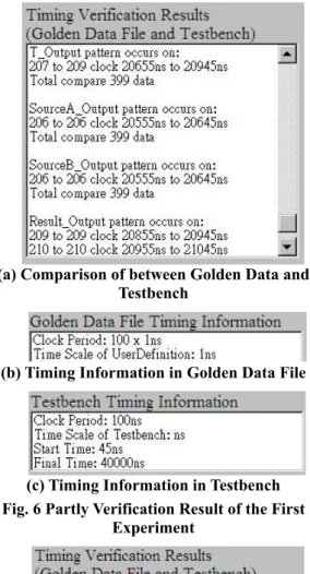
Fig. 6(a) shows comparing result between golden data and testbench. EFVT also shows timing information of golden data and testbench as shown in Fig. 6(b) and 6(c), respectively. We know system designed correctly after observing verification result.
During phase 2, the simple CPU performs data moving from source memory A into result memory 25 times. In order to demonstrate the feasibility of our
(a) Comparison of between Golden Data and Testbench
(b) Timing Information in Golden Data File
(c) Timing Information in Testbench Fig. 6 Partly Verification Result of the First
Experiment
(a) Running Results in Result Memory by EFVT
(b)Running Results in Source Memory A by EFVT Fig. 7 Partly Verification Result of the Second
Experiment
TABLE III Comparisons of Design Target Design Target Our Proposed Huang [6]
Abstraction Level Signal Level System Level Objective FPGA System
Prototyping System Level Design Evaluation Bus Transaction
Description Method
Text File PSL[8]
TABLE IV Comparison of between EFVT and FVT
Function EFVT FVT[7]
Functional verification among golden
data, testbench and Chipscope Pro Yes Yes Error rates report of functional
verification Yes Yes
Verification for bus transaction Yes not support Timing information display Yes not support Point out errors or questionable
transitions easy hard
Debugging effort less more verification tool, we insert a bug into the ALU. EFVT will find the bug. Testbench file is generated by ModelSim 6.1f. Next, we inputted golden data and testbench file into EFVT.
Partly verification result is shown in Fig. 7(a) for conciseness. Actually, EFVT lists moving data 24 times due to bug in the ALU. Fig. 7(b) shows the source memory A that does not output data during clock 1 to 8. If system were designed correctly, EFVT would find moving data 25 times during clock 1 to 200. EFVT finds whether testbench against golden data.
In Table III, we compare the design target between our proposed tool and Huang[6]. Huang’s approach focuses on system level design and describes bus protocol in PSL[8]. Our tool verifies bus transaction for FPGA system prototyping and deals with detail signal transition in bus protocol.
Our proposed tool also improved the previous work [7]. Table IV shows the differences between EFVT and FVT. EFVT not only performs previous verification work but also verifies bus transaction between golden data and testbench. Timing information of golden data and testbench can be displayed in EFVT. Finally, designer spends less effort to find bug with EFVT.
6. Conclusions
A design of automatic timing verification tool for FPGA systems is presented. An efficient verification algorithm is proposed to reduce the debugging time in a design FPGA system. We also design a friendly graphic user interface for system designer to use easily. Finally, a simple CPU design example is shown to demonstrate the feasibility of proposed tool.
From experimental results shown that the proposed tool has improved preliminary proposed tool [7].
References
[1] P. Rashinkar, P. Paterson and L. Singh, Systm-On-a-Chip Verification: Methodology and Techniques, 2nd ed., Kluwer Academic, 2001.
[2] Y. Nakamura, K. Hosokawa, I. Kuroda, K.
Yoshikawa and T. Yoshimura, “A fast hardware/software co-verification method for systern-on-a-chip by using a C/C++ simulator and FPGA emulator with shared register communication,” Proceeding of the 41st Design Automation Conference, pp. 299-304, Jun. 7-11, 2004.
[3] Y.-F. Lin, X.-Y. Zeng, M. Wu, J. Chen, R. Bao,
“New methods of FPGA co-verification for system on chip (SoC),” Proceeding of ASICON Conference, Vol. 1, pp. 169-172, Oct. 2005.
[4] C. L. Chuang, D. J. Lu, and C. N. J. Liu, “A snapshot method to provide full visibility for functional debugging using FPGA,” Proceeding of the 13th Asian Test Symposium (ATS2004), pp.
164-169, Nov. 15-17, 2004.
[5] K.-S. Oh, S.-Y. Yoon, and S.-I. Chae, “Emulator environment based on an FPGA prototyping board,” Proceeding of Rapid System Prototyping, pp. 72-77, Jun. 2000.
[6] Y. L. Huang, C. Y. Wang, R. Yeh, S. C. Chang, and Y. C. Chen, “Language-Based High Level Transaction Extraction on On-chip Buses,”
Proceeding of the International Symposium on Quality Electronic Design (ISQED’06), pp. 27-29, Mar. 2006
[7] T. Y. Lee, Y. H. Fan, S. C, Yen, C. C. Tsai and R. S.
Hsiao, “An Integrated Functional Verification Tool for FPGA Systems,” IEEE Computer Society of the 2nd International Conference on Innovative Computing, Information and Control (ICICIC’07), Sep. 5-7, 2007.
[8] Accellera. “Property Specification Language Reference Manual Version 1.01,” 2003.
![TABLE III Comparisons of Design Target Design Target Our Proposed Huang [6]](https://thumb-ap.123doks.com/thumbv2/9libinfo/9501947.596128/5.892.105.440.128.473/table-comparisons-design-target-design-target-proposed-huang.webp)
