國立臺灣大學電機資訊學院光電工程學研究所 博士論文
Graduate Institute of Photonics and Optoelectronics College of Electrical Engineering and Computer Science
National Taiwan University Doctoral Dissertation
利用親水性質發展之自組式微透鏡與以離子導電高分子金屬 複合物製備之低致動電壓可形變面鏡
Self-assembly microlens by hydrophilic effect and low actuation-voltage deformable mirror by ionic polymer metallic
composite
魏祥鈞
Hsiang-Chun Wei
指導教授:蘇國棟 博士
Advisor: Guo-Dung John Su, Ph.D.
中華民國 100 年 12 月
誌謝
在博士班的生涯中,我要感謝許多人給予我的協助,不管是研究、課業、生 活或是精神上的指導或支持,都仰賴於你們的幫忙,我才有辦法完成這篇論文。
因此,我很感謝這段時間曾經給我幫助的人以及不斷鼓勵我的人。
首先要感謝這幾年來不斷用心給予指導及鼓勵的指導教授蘇國棟博士,當實 驗遇到瓶頸時教授提供的許多建議、支持我在實驗上的各種嘗試,讓我學習到對 研究的應有的態度與方法。感謝教授在學生投稿時不厭其煩地幫我修改內容,讓 文章可以順利地刊載在期刊上。除此之外,也很感謝教授在生活上給予的關心,
學生特別感到貼心。還有諸位口試委員們,林晃巖博士、趙基揚博士、馮國華博 士、許巍耀博士,你們提供的寶貴意見,讓我受益良多。此外,我也要感謝元亨、
竟偉、孟萱在光學系統設計上,還有美妏在微透鏡陣列及波前感測器的努力。研 究團隊中的煜達、晉亨、鄭維、豐德(Te)、適安,感謝你們耐心地和我一起做實驗,
一次又一次的討論之中,我也有許多寶貴的收穫,同時也感謝你們幫忙把相關的 技術傳承下去。另外也感謝台大機械所學弟丞家對於化學電鍍的指導。
感謝已畢業的怡文、哲瑜、美妏、以樵,在無數個熬夜生活中,你們的相伴 讓我不是一人孤軍奮戰。也要感謝實驗室的成員,包含學長紹軒、欣達,以及現 在一起在實驗室的璿閔、聖原、旌寶、建綸、鄭維、晉亨、豐德(Te)、裕閎、佳勳、
柏宇、沐豪、柏彰、宇翔 、威志、適安、建任、以晨、惠凱、舜齡、怡瑄、緯詳、
偉廷。還有許多已經畢業的成員及其他實驗室的朋友們、光電所所辦小姐和所學 會的夥伴,雖然無法列舉,你的幫助我會銘記在心,也因為有你,讓我在學校的 生活增添了許多風味。
本論文獻給我最要感謝的最親愛的父母還有姐姐,多年來給我經濟還有精神 上的支持,在我求學的過程中不斷的鼓勵我、安慰我,無論我多沮喪都陪伴在我 身邊。還有女友孟潔多年的相伴、包容、關懷。若將來我能有所成就,將會是你
中文摘要
在本篇論文中,我們的研究涵蓋了兩大主題,分別為微透鏡陣列(microlens array)以及可形變面鏡(deformable mirror)。經由整合此二元件與一般光學元件後,
發展光學系統於不同的應用。
自組式微透鏡陣列(self-assemble microlens array),利用了紫外線臭氧清潔機將 SU-8 負型光阻表面改質,產生週期性排列的親水性區域,再利用表面張力將稀釋 過後的 SU-8 光阻自行聚集在此親水性區域之中,進而形成球面的液態平凸透鏡,
最後經由紫外光的固化後成了固體的微透鏡陣列。SU-8 光阻具有良好的化學穩定 性及機械強度,其光學吸收率非常低,加上基板使用的是透明玻璃,所以製作出 來的微透鏡陣列是穿透式的,不須要再另外經過翻模的方式來製作,大幅簡化了 製作的流程及減少製程時間。此方法具有低成本、低溫、省時之特點。另外,SU-8 光阻本身是極性材料,藉由外加的電場可以增加表面的曲率,藉此進一步可以產 生更短焦距的微透鏡,同時也使表面的粗糙度降低,提高其光學性質。同時,使 用這種方法,我們可以精準地將微透鏡製作在發光二極體(LED)上,提高提取效率 並增加發散角。另外,藉由實驗室發展的雙層熱回流式長焦長微透鏡陣列,我們 發 展 了 更 為 靈 敏 、 動 態 範 圍 更 廣 的 薛 克 - 哈 特 曼 波 前 感 測 器 (Shack-Hartmann wavefront sensor),同時針對長焦距及短焦距的影響與商用的感測器做比較。
我們利用了實驗室發展的微機電有機可形變面鏡 (micro electro mechanical systems organic deformable mirror),配合光學鏡頭元件設計了可變對焦平面的光學 模組,搭配 Tenengrad 影像處理方法及百分率降幅方法(percentage drop method)組
面鏡的驅動電壓較高(約 150 伏特),所以我們進而採用了高分子致動器-離子導電 高分子金屬複合物(ionic-conductive polymer metal composite, IPMC),其具有低致動 電壓與大位移量的特性。我們藉由發展此材料的灰盒子理論,搭配 ANSYS 有限元 素分析軟體,設計了齒輪狀的離子導電高分子金屬複合物可形變面鏡(gear shaped IPMC DM),其特點為低致動電壓及較廣的焦距變化。同時由於其可雙向致動的特 性,可製作出同時具有聚焦及散焦能力的可形變面鏡。
最後,我們希望此篇論文可以啟發相關的研究,並對後續的發展有些許貢獻。
關鍵字: 微透鏡、SU-8 光阻、親水性、波前感測器、可形變面鏡、離子導電高分 子金屬複合物。
ABSTRACT
In this dissertation, there are two major topics of microlens array (MLA) and deformable mirror (DM). By integrating these two components and ordinary optical component, we developed different optics system in different applications.
Self-assembled microlens array was fabricated by hydrophilic effect using Ultraviolet (UV)/ozone modification on glass substrate. The modification on SU-8 photoresist produced periodic array of hydrophilic areas on the surface by the use of shadow mask. Afterwards, the substrate was dipped in and out of diluted SU-8 photoresist. Therefore, the liquid self-assembled MLA was formed. Finally, the solid MLA was cured by UV light. SU-8 photoresist has good chemical and mechanical strength, so it is suitable for MLA. Besides, the fabricated MLA is transparent so that there has no need for etch transferring. It decreases the process complexity a lot.
Meanwhile, because of the polar molecular of SU-8 photoresist, the curvature of the microlens can be enlarged by applying external electric field. The surface roughness could be improved as well. This method provides a low cost, low time consumption, no etch transfer, low temperature, and no photo lithography method to fabricate MLA. We applied this method to fabricated microlens on a light emitting diode (LED) chip with precisely alignment. That improved the extraction efficiency and increased the viewing angle. Besides, we developed a more sensitive and larger dynamic ranged Shack-Hartmann wavefront sensor by using the developed long focal length MLA using double layer thermal reflow method. We also compared it with the commercial product.
We developed a thin autofocus camera module by using the developed micro electro mechanical systems (MEMS) organic deformable mirror (DM). It included a
sharpness function and percentage-drop method. Besides, because of the high actuation voltage (~150 V), we adopt an ionic-conductive polymer composite to fabricate DM.
IPMC is a polymer actuator with the advantage of low actuation voltage and large displacement. We built a simplified grey box model and simulate the deformation shape by using finite element method software, ANSYS® . A gear shaped IPMC DM was designed and demonstrated. It had the advantage of low actuation voltage and large optical power. Meanwhile, because of the bi-directional deformation ability, the DM with both positive and negative optical power was achieved.
Finally, we believe these research topics could inspire the related researchers and might have some benefit to the human.
Keywords: microlens array, SU-8 photoresist, hydrophilic, wavefront sensor,
deformable mirror, ionic-conductive polymer metal composite.CONTENTS
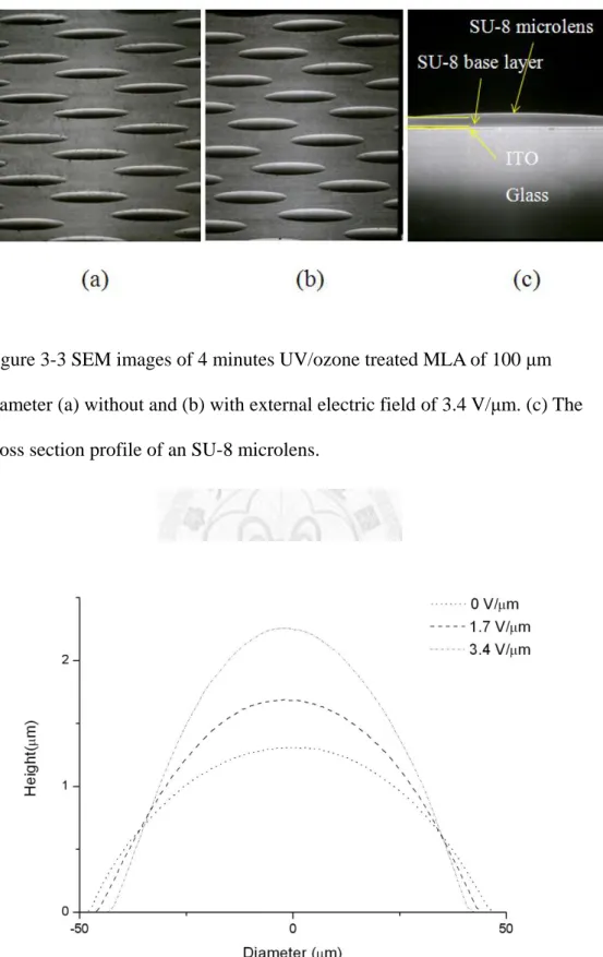
論文口試委員審定書
誌謝 ... I 中文摘要 ... II ABSTRACT ... IV CONTENTS ... VI LIST OF FIGURES ... X LIST OF TABLES ... XVIII
Chapter 1 Dissertation Organization & Introduction... 1
1.1 Dissertation organization ... 1
1.2 General introduction ... 2
1.2.1 Review of microlens array fabrication technologies ... 2
1.2.2 Review of Shack-Hartmann wavefront sensor ... 6
1.2.3 Review of method to achieve auto-focus function ... 9
References ... 13
PART I MICROLENS ARRAY ... 14
Chapter 2 Using Hydrophilic Effect to Fabricate Self-Assembled Microlens Array by UV/ozone Modification ... 15
2.1 Introduction ... 16
2.2 Fabrication Process ... 17
2.3 Experimental Results and Discussions ... 19
2.4 Conclusions ... 27
References ... 28
Hydrophilic Effect and Electric Fielding Pulling ... 30
3.1 Introduction ... 31
3.2 The working mechanism ... 32
3.3 Fabrication processes ... 35
3.3.1 SU-8 photoresist base layer ... 36
3.3.2 UV/ozone treatment ... 37
3.3.3 Dipping in and out of diluted SU-8 photoresist ... 37
3.3.4 Applying electric field and UV curing ... 38
3.4 Experimental results and discussions ... 39
3.5 Conclusions ... 48
References ... 49
Chapter 4 Self-assembled microlens on top of light emitting diodes using hydrophilic effect for improving extraction efficiency and increasing viewing angle ... 51
4.1 Introduction ... 52
4.2 The working mechanism ... 53
4.3 Fabrication process ... 56
4.4 LED encapsulation ... 56
4.4.1 SU-8 photoresist base layer ... 57
4.4.2 UV/ozone treatment ... 57
4.4.3 Dipping in and out of diluted SU-8 photoresist & UV curing ... 58
4.5 Optical System Simulation and experimental results ... 59
4.6 Conclusions ... 68
References ... 69
5.2 Design of Double Layer Microlens Array ... 73
5.3 Fabrication Processes and Results ... 75
5.4 Wavefront Sensor Computing Algorithm and Measurement Results79 5.5 Conclusions ... 88
References ... 90
PART II DEFORMABLE MIRROR ... 91
Chapter 6 Controlling a MEMS Deformable Mirror in a Miniature Auto-Focusing Imaging System ... 92
6.1 Introduction ... 93
6.2 Deformable Mirror and Optical System Design ... 94
6.3 Tenengrad Method and Percentage-Drop Searching Algorithm ... 101
6.4 Experiment Results and Discussion ... 105
6.5 SUMMARY ... 109
References ... 111
Chapter 7 Thin autofocus camera module by a large-stroke micromachined deformable mirror ... 113
7.1 Introduction ... 114
7.2 Optical System Design with Autofocus Function ... 115
7.3 Device Fabrication and Experimental Results ... 118
7.4 Conclusion ... 127
References ... 128
Chapter 8 A Low Voltage Deformable Mirror using Ionic-conductive Polymer Metal Composite ... 129
8.1 Introduction ... 130
8.3 FEM simulation model of cantilever beam ... 133
8.4 Simulation model and experimental verification ... 137
8.5 Gear shaped IPMC and experimental result ... 139
8.6 SUMMARY ... 144
References ... 146
Chapter 9 Conclusions and Future Work ... 147
9.1 Dissertation conclusions ... 147
9.1.1 Microlens arrays ... 147
9.1.2 Deformable mirrors ... 148
9.2 Suggestions for future work ... 149
9.2.1 The focus microlens on LED by using thicker PDMS. ... 149
9.2.2 The microlens application on concentrated solar cell... 150
9.2.3 The improvement of surface roughness for IPMC DM by the use of PDMS buffered layer ... 151
Publication List ... 153
LIST OF FIGURES
Figure 1-1 The microlens fabrication techniques and their development timeline [1]... 4 Figure 1-2 The different fabrication process steps for refractive reflow photoresist microlenses: (a) patterning of the photoresist layer; (b) development of the exposed regions; (c) melting of the cylindrical islands. [1]... 5 Figure 1-3 Basic fabrication process for arrays of spherical microlenses with deep lithography with protons: irradiating the PMMA layer through a mask and applying a vapour on one surface of the irradiated sample are the basic processing steps for the fabrication of 2D arrays of stable and uniform spherical microlenses. [1] ... 5 Figure 1-4 Principle of laser ablation. [1]... 6 Figure 1-5 Schematic of the droplet-on-demand microjet system ... 6 Figure 1-6 (a) Scheiner’s disk produces double retinal images of a single object if the eye is ametropic. (b) Scheiner’s disk was used by Smirnov to create a subjective aberrometer. [8] ... 7 Figure 1-7 A Scheiner’s disk with multiple holes is called a Hartmann screen and may be used to construct an objective aberrometer. [8] ... 8 Figure 1-8 An aberrated wavefront is incident on a lenslet array. Each spot is shifted from its on-axis position, shown in blue, by an amount proportional to the average phase gradient across its lenslet [10]. ... 8 Figure 1-9 The schematic drawing of auto-focus system with a moving component. ... 9 Figure 1-10 The scheme of auto-focus system without moving component. ... 10 Figure 1-11 Lens like phase retardation when applying voltage on LC cell. [14] (a) No
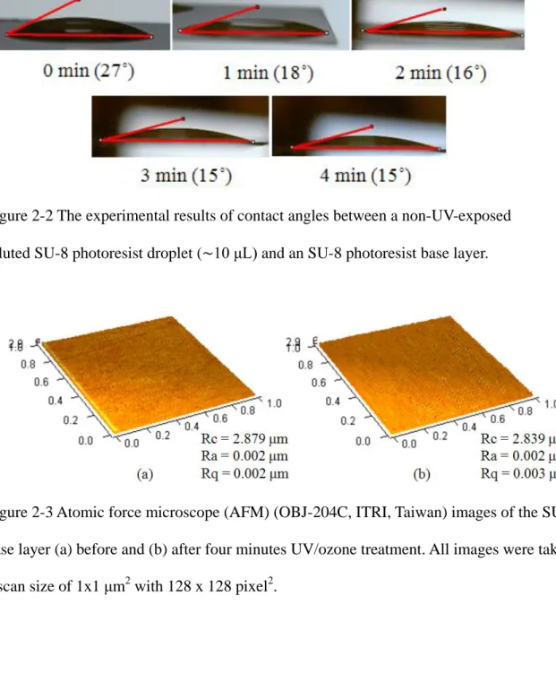
(c) result a negative optical power lens like phase retardation. ... 11 Figure 1-12 Structure of liquid lens developed by Varioptic. [17] ... 12 Figure 1-13 The disadvantage of liquid lens is that coma aberration may occur due to gravitational pull. [16] ... 12 Figure 2-1 The fabrication process of SU-8 photoresist MLA using hydrophilic effect under UV/ozone treatment. ... 18 Figure 2-2 The experimental results of contact angles between a non-UV-exposed diluted SU-8 photoresist droplet (∼10 μL) and an SU-8 photoresist base layer. ... 21 Figure 2-3 Atomic force microscope (AFM) (OBJ-204C, ITRI, Taiwan) images of the SU-8 base layer (a) before and (b) after four minutes UV/ozone treatment.
All images were taken at a scan size of 1x1 μm2 with 128 x 128 pixel2. ... 21 Figure 2-4 The contact angles for different UV/ozone treatment time and different shadow mask openings. The shadow mask openings were 50 μm, 100 μm, and 200 μm in diameters. ... 22 Figure 2-5 Focal length versus UV/ozone treatment time. ... 22 Figure 2-6 The MLAs fabricated using 100-μm diameter shadow mask. (a) Optical microscopy and (b) the corresponding focus points with (c) intensity profile for four minutes UV/ozone treatment time. (d) Zoomed image of the optical intensity profile. ... 24 Figure 2-7 The SEM of (a) microlenses of 100 μm diameter under one minute UV/ozone treatment time. (b) the cross section profile of one minute treated
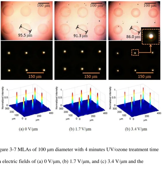
Figure 3-1 The schematic of the presented fabrication of the SU-8 MLA.(a) UV/ozone treatment (b) Hydrophilic zones is presented (c) Dip out from the diluted SU-8 photoresist solution (d) Apply the external voltage. ... 35 Figure 3-2 The fabrication process. (a) An SU-8 base layer on the ITO glass (b) Contact shadow mask (c) UV/ozone treatment (d) remove shadow mask (e) Hydrophilic zones presented (f) Dip out from diluted SU-8 photoresist solution (g) Apply the external voltage. ... 39 Figure 3-3 SEM images of 4 minutes UV/ozone treated MLA of 100 μm diameter (a) without and (b) with external electric field of 3.4 V/μm. (c) The cross section profile of an SU-8 microlens. ... 41 Figure 3-4Surface profile of microlens via different electric fields. ... 41 Figure 3-5 Lens profile and the corresponding best fit sphere of the fabricated microlens (a) without applied electric field, (b) with 1.7 V/μm, and (c) 3.4 V/μm measured by probe-type surface analyzer. The circles show measure points and solid red lines are best fit spheres. ... 42 Figure 3-6 The experimental results of UV/ozone treatment time versus contact angle.
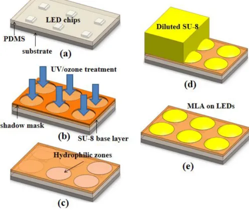
The black solid squares are the experimental results of contact angles between a non-UV-exposed diluted SU-8 photoresist droplet and an SU-8 photoresist base layer. ... 44 Figure 3-7 MLAs of 100 μm diameter with 4 minutes UV/ozone treatment time via electric fields of (a) 0 V/μm, (b) 1.7 V/μm, and (c) 3.4 V/μm and the corresponding focus beam spots. ... 47 Figure 4-1 The schematic of the presented fabrication of the SU-8 MLA. (a) Encapsulating the LED chips by PDMS. (b) UV/ozone treatment through
diluted SU-8 solution. (e) UV curing. ... 55 Figure 4-2 The fabrication process. (a) The bared LED chip. (b) Wire bonding and PDMS encapsulation. (c) PDMS hardening. (d) A layer of SU-8 base layer.
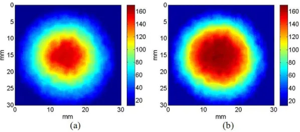
(e) UV/ozone treatment through shadow mask. (f) Removing the shadow mask. (g) Dipping out from diluted SU-8 solution. (h) UV curing. ... 59 Figure 4-3 The optical system of microlens on LED. ... 60 Figure 4-4 The simulation result of luminance map (30 mm x 30 mm). (a) Without microlens (b) With microlens. ... 61 Figure 4-5 (a) The experimental results of contact angles between a non-UV-exposed diluted SU-8 photoresist droplet and an SU-8 photoresist base layer. (b) The experiment setup of Sessile Drop method. ... 62 Figure 4-6 (a) The SEM photograph of 200-μm diameter MLA under three minutes UV/ozone treatment time. (b) The cross section profile of an SU-8 microlens. ... 63 Figure 4-7 The optical microscope image of fabrication result. (a) The LED chip with aluminum (Al) wire bonding. (b) The 200-μm diameter microlens on LED.
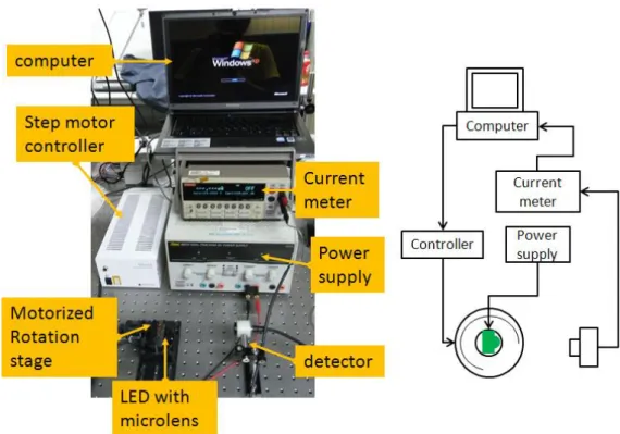
(c) The clear stereo microscope image on both LED chip and microlens. (d) The tile view of the stereo microscope image of the microlens on LED. .... 65 Figure 4-8 The measurement setup of the angular light field distribution. ... 66 Figure 4-9 The normalized angular distribution of light intensity (from -90 to 90 degree).
It improved the extraction efficiency of 15 % and 28% in maximum and total accordingly, and increased the viewing angle of 17 degree (θ1/2). ... 67
lines) and (b) our new method (solid lines). ... 74 Figure 5-3 Fabrication steps of long-focal length MLA. (a)PR cylinders (b)Thermal reflow (c)PDMS molding (d)Release PDMS mold (e)Drop UV-resin &
attach glass(f)UV curing. ... 76 Figure 5-6 SEM image of the UV-resin MLA (a) without and (b) with the second layer of PDMS. ... 77 Figure 5-7 The focused spot images (above) and their intensity distribution (below) of
(a) circular lens quadratic grid MLA, (b) circular lens hexagonal grid MLA,
(c) hexagonal lens MLA, and (d) square lens MLA. ... 78
Figure 5-8 The experiment setup for measuring a wavefront aberration of testing lens (PAL) by using our fabricated MLA and SHWS. ... 82 Figure 5-9 (a) Focal spots image of the reference wavefront, (b) focal spots image of the aberrated wavefront, and (c) detection picture of image spots for reference beam and distorted beams. ... 83 Figure 5-10 Wavefront measurement results of (a) PAL and (b) PCX by our SHWS (above) and commercial SHWS (below). ... 84 Figure 5-11 Wavefront measurement results of defocus by using (a) long focal length (UV-resin) and (b) shorter focal length (SU-8) MLA as our SHWS lenslet component. ... 88 Figure 6-1 Structure of MEMS deformable mirror [(a) Top electrode plate; (b) Bottom electrode plate; (c) Encapsulation]. ... 96 Figure 6-2 Deformable Mirror [(a) Without an applied voltage; (b) With an applied voltage] ... 97 Figure 6-3 Relation between the optical power of the deformable mirror and the appliedFigure 6-4 Optical system layout of the reflective auto-focusing camera module. ... 99
Figure 6-5 Picture of the actual optical camera module. ... 99
Figure 6-6 Modulation transfer function (MTF) of the optical system. ... 101
Figure 6-7 Focus value vs. applied voltage at different object distances. ... 104
Figure 6-8 Percentage-drop searching algorithm. ... 105
Figure 6-9 Setup of the auto-focusing camera system. ... 107
Figure 6-10 Images taken at different object distances and with optimized applied voltages. ... 108
Figure 6-11 Experimental results of percentage-drop Searching. The standard deviations are 0.31 and 0.02 when the object distances were 200 mm and 50 mm respectively. ... 109
Figure 7-1 (a) Optical system design in reflective form, and (b) its modulation transfer function (MTF) when a MEMS deformable mirror is flat for far objects .. 116
Figure 7-2 (a) Image simulation results of Lady Lenna, and (b) its modulation transfer function (MTF) when a MEMS deformable mirror is actuated for near objects. ... 117
Figure 7-3 Device fabrication processes for a top polymer membrane and a bottom electrode. ... 120
Figure 7-4 Schematic drawings and photos of a fabricated MEMS deformable mirror device. ... 121
Figure 7-5 Diopter changes versus applied voltage of the polymer MEMS DM. ... 122
Figure 7-6 Assembly 3D drawings of an autofocus module ... 124
Figure 8-1 The schematics of the IPMC network and (b) the molecular formula of Nafion. ... 133 Figure 8-2 The simplified model with constant stress field which would be implied to the FEM model. ... 134 Figure 8-3 ANSYS® structure model of IPMC ... 135 Figure 8-4 ANSYS® element model of IPMC ... 135 Figure 8-5 FEM simulation which varied the length (L) and width (w) of IPMC and the half thickness (h) of Nafion with constant surface force (P = 100 Pa) ... 137 Figure 8-6 Deformation shape of double side confinement. (a) simulation (b) experiment. (These figures show IPMC with and without applied voltage)138 Figure 8-7 The black dots are experimental results of tip displacement vs. applied
voltage. And the solid line is simulation result by curve fitting, where C2 is 60000 (Pa*m/V). ... 139 Figure 8-8 The gear shaped IPMC design. ... 141 Figure 8-9 The IPMC process flow.(a) ion exchange polymer formation and pre-process;
(b) initial compositing; (c) surface electrode growing;(d) shape cutting. .. 141 Figure 8-10 (a) The Picture of experimental demonstration of the new deformable mirror. (b) The deformation simulated by ANSYS® . ... 143 Figure 8-11 The intensity profile of the laser beam spot with non-actuated IPMC (non-focused) and actuated IPMC (focused). ... 143 Figure 8-12 The surface profile using white light interferometer. ... 144 Figure 9-1 The principle of the LED light beam manipulation by using PDMS thickness.150 Figure 9-2 The small lens array with triangular prism model ... 151 Figure 9-3 IPMC DM with PDMS buffered layer. ... 151
sheet(b) clamped by frames (c) spin PDMS and coat copper reflector (d) laser cutting (e) the section of PDMS modified gear shaped IPMC DM. .. 152
LIST OF TABLES
Table 2-1 The footprint diameters of MLAs. ... 23
Table 2-2 The summarized results of fabricated MLAs. ... 26
Table 3-1 The focal length, sag height, and radius of curvature of fabricated MLA by different UV/ozone treatment time without external electric field enhancement. ... 45
Table 3-2 The summarized results of the fabricated MLA. ... 48
Table 5-1 Lens arrangement versus fill factor for 20 m of lens gap. ... 78
Table 5-2 Methods for increasing the focal length of MLA. ... 79
Table 5-3 The comparison of wavefront measurement by our SHWS and commercial SHWS. ... 86
Table 8-1 Physical parameters of different materials ... 136
Table 8-2 The comparison of different technologies. ... 144
Chapter 1 Dissertation Organization & Introduction
1.1 Dissertation organization
The dissertation consists of two parts. From chapter 2 to chapter 5 are described to the microlens. From chapter 6 to chapter 8 are described to the deformable mirror.
Chapter 9 is the conclusion and future works. Each chapter is a research topic.
Meanwhile, some topics were published in journals.
In chapter 2, we presented a self-assembled microlens array (MLA) fabricated by use of the hydrophilic effect under ultra-violet (UV)/ozone treatment. This method provides a fast, simple, and low cost process. It does not require lithography or etch-transfer processes. (This work was published in Photonics Technology Letters,
IEEE, vol. PP, pp. 1-1, 2011).
In chapter 3, we present a variable and self-assembled spherical microlens array (MLA) fabricated by the use of the hydrophilic effect under ultra-violet (UV)/ozone treatment. The optical power and surface roughness of MLA was further enhanced by applying external electric field. (This work was accepted in Journal of Micromechanics
and Microengineering at 2011. 11. 25).
In chapter 4, we propose a self-assembled microlens arrays (MLAs) on top of light emitting diodes (LEDs) based on hydrophilic effect under ultraviolet (UV)/ozone treatment to improve extraction efficiency and to increase viewing angle. (This work
was submitted to Journal of Display Technology 2011.12.16).
In chapter 5, we present the design and fabrication of long focal length MLA based on a double layer structure for optical wavefront sensing applications. A longer focal
In chapter 6, we discussed a new auto-focusing camera system, which features a reflective optics design based on a polymer MEMS deformable mirror and a control program. (This work was published in IEEE Transactions on Control Systems
Technology, vol. PP, pp. 1-5, 2011).
In chapter 7, we propose a second generation of thin autofocus system using a large stroke MEMS (micro-electro-mechanical systems) deformable mirror which has the potential to downscale the size and to minimize chromatic aberration. (This work
was published in Optics Express, vol. 18, pp. 11097-11104, 2010).
In chapter 8, we design the gear shaped IPMC type deformable mirror that is simulated by finite element method and then demonstrate its focus-varying function. It requires less than 5 volts to achieve 20 diopters.
In chapter 9, we draw conclusions of previous chapters and show the suggestions to the future work.
1.2 General introduction
1.2.1 Review of microlens array fabrication technologies
Over the last 20 years several research groups and industrial research laboratories have therefore been focusing their attention on the development of fabrication techniques for refractive microlenses and microlens arrays [1]. In the 17th century, Robert Hooke and Antonie van Leeuwenhoek both developed techniques to make small glass lenses for use with their microscopes. Hooke melted small filaments of Venetian glass and allowed the surface tension in the molten glass to form the smooth spherical surfaces required for lenses, then mounting and grinding the lenses using
into materials such as photoresist or UV curable epoxy and melting the polymer to form arrays of multiple lenses [2][3].
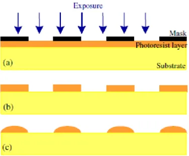
A wide variety of applications of very small lenses grows interest in the study of arrays. In 1908, Gabriel Lippmann proposed numerous applications for small lens arrays including the recording of three dimensional pictures by taking photographs through biconvex arrays. A variety of manufacturing techniques have been proposed and studied. However, one of the simplest and most elegant techniques was described by Popovic et al (1988). He fabricated cylindrical islands of photoresist using by photolithography and then melted them so that surface tension caused PR to adopt hemispherical form.
Fabrication of MLAs prototype is very important as it defines all characteristics of MLAs. It has been long known that fabrication methods of MLAs can be achieved by thermal reflow [2], laser beam written microlenses [4], DLP (deep lithography with protons) [5], laser ablation [6], microjet printing [7], and reactive ion etching which are shown in Figure 1-1.
Figure 1-2 to Figure 1-5 shows the process flow of the microlens fabrication techniques [1]. Some methods are relatively inexpensive and are based on existing technologies while others require dedicated processing tools and/or new materials with special properties. Most of these microlens fabrication methods yield MLAs that satisfy many of the optical quality requirements. They differ however in that some fabrication methods are more suitable either for rapid prototyping, for mass fabrication or for monolithic integration than others.
Figure 1-1 The microlens fabrication techniques and their development timeline [1].
Figure 1-2 The different fabrication process steps for refractive reflow photoresist microlenses: (a) patterning of the photoresist layer; (b) development of the exposed regions; (c) melting of the cylindrical islands. [1]
Figure 1-3 Basic fabrication process for arrays of spherical microlenses with deep lithography with protons: irradiating the PMMA layer through a mask and applying a vapour on one surface of the irradiated sample are the basic processing steps for the fabrication of 2D arrays of stable and uniform spherical microlenses. [1]
1.2.2 Review of Shack-Hartmann wavefront sensor
Nearly 400 years ago, Christopher Scheiner, a professor at the University of Ingolstadt, used a simple device known as the Scheiner Disk to demonstrate the focusing ability of the human eye [8]. Scheiner’s experiments applied a single point of light through an opaque disk perforated with two pinholes and showed that two retinal images will be formed by imperfect eyes as showed in Figure 1-6(a) [8]. An
Figure 1-5 Schematic of the droplet-on-demand microjet system used to fabricate refractive microlenses. [1]
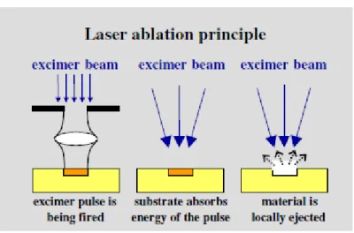
Figure 1-4 Principle of laser ablation. [1]
moveable light source for the outer pinhole as illustrated in Figure 1-6(b) [8] and adjusting the moveable source horizontally and vertically until the light intersects at the retina and the patient reports seeing a single point of light. The ray aberration of the eye at the given pupil point is measured from the displacement distances having made by this adjustment. This subjective aberrometer was first introduced by Smirnov and has been used in visual optics research the past 50 years.
Johannes Hartmann, a professor in Potsdam, at the beginning of the 20th century developed his famous Hartmann screen. Additional holes are constructed in Scheiner’s disk to convert the Scheiner-Smirnov subjective technique into an objective aberrometer.
On the contrary, the direction of the light propagation is reversed by placing a spot of light on the retina. This spot then becomes a point source which radiates back out of the eye as illustrated in Figure 1-7. Each aperture in the Hartmann screen isolates rays emerging from the eye through the different part of the pupil. These emerging rays intersect a sensor to detect the horizontal and vertical displacement of each ray from the
Figure 1-6 (a) Scheiner’s disk produces double retinal images of a single object if the eye is ametropic. (b) Scheiner’s disk was used by Smirnov to create a subjective aberrometer. [8]
Eighty years later, Dr. Roland Shack replaced the holes in Hartmann screen by lenses. By adding lenses, the light passing through the apertures will be broken into many individual beams and concentrated to focal spots which are shown in Figure 1-8, and detected by the image sensor. The derivative of the wavefront optical path difference (OPD) map produces wavefront slopes, the integration of wavefront slopes produces wavefront OPD maps [9].
Figure 1-8 An aberrated wavefront is incident on a lenslet array. Each spot is shifted from its on-axis position, shown in blue, by an amount proportional to the average Figure 1-7 A Scheiner’s disk with multiple holes is called a Hartmann screen and may be used to construct an objective aberrometer. [8]
1.2.3 Review of method to achieve auto-focus function
There are several ways to vary effective focus length of image system to achieve auto-focus function. They can roughly be classified to two groups, system with moving components and system without moving components. These techniques will be introduced in this section
System with moving components is characteristic with that it has moving components to move lens or lens group back and forth to vary effective focal length.
Therefore, the system can focus on object located at difference distance from lenses module, as shown in Figure 1-9.
The principle can be illustrated by this equation [11]:
2 1 2 1
1 1 1
f f
d f
f
f (1.1) which states the effective focal length, f, of a system combined with two lenses at a distance of d and whose focal length are f and f individually. According to equation
Figure 1-9 The schematic drawing of auto-focus system with a moving component.
Motor has been used for camera with auto-focus or zoom function for a long time, but with the trend to downscale of camera built-in portable device, especially the thin thickness, miniaturizing camera module becomes important. Therefore, small motor design has appeared, for instance, miniature stepping motor, piezoelectric motor, and voice and coil motor.
To downscale purpose, more and more techniques are proposed to achieve auto-focus function without any moving components. The advantage of system without moving components is that the total track length has the potential to become shorter than system with moving components since there need no space for moving component to move forth and back. The system design will become more flexible and it is easier to save space for designer. The concept of system without moving components is that tuning optical power of one or more optical elements to change system’s effective focal length. Figure 1-10 is a simple schematic of system to achieve auto-focus function without moving components. Lens 1 and Lens 3 are the fixed optical power element, and Lens 2 is tunable optical power element. Tuning optical power of Lens 2 can change effective focal length of system.
Figure 1-10 The scheme of auto-focus system without moving component.
Liquid crystals (LCs) have applications for light spatial modulators, waveguides, phase modulators, liquid crystal switches, light detectors, and displays. In recent years, it has been reported that LCs has the capability of auto focus function for lenses application. Akita University has developed a technique which is a liquid crystal lens with focal length variable from negative to positive [12-14]. The lens like phase retardation profile from positive to negative lens can be obtained by varying the two voltages appropriately, as show as Figure 1-11. Therefore, the LC cell acts as a lens whose focal length can be control by the voltages.
Another element has used to achieve auto-focus function without moving component is liquid lens. Liquid lenses developed by Varioptic [15-17]. The mechanism is based on the phenomenon of electro-wetting. Figure 1-12 is the schematic of the design of Varioptic. Two immiscible liquids, water and oil, one is used as conducting layer and the other is used as insulating layer, are contained in the two transparent
(a) (b) (c)
Figure 1-11 Lens like phase retardation when applying voltage on LC cell. [14] (a) No voltage apply. (b) result a positive optical power lens like phase retardation. (c) result a negative optical power lens like phase retardation.
oil, is determined by the balance of the surface tension produced by the two liquids.
On the other words, the focal length of the liquid lens is controlled by varying applied voltage. However, its disadvantage is that coma aberration may occur due to gravitational pull, as shown in Figure 1-13
Figure 1-12 Structure of liquid lens developed by Varioptic. [17]
Figure 1-13 The disadvantage of liquid lens is that coma aberration may occur due to gravitational pull. [16]
References
[1] H. Ottevaere, R. Cox, H. P. Herzig, T. Miyashita, K. Naessens, M. Taghizadeh, R.
Volkel, H. J. Woo, and H. Thienpont, “Comparing Glass and Plastic Refractive Microlenses Fabricated with Different Technologies,” J. Opt. A: Pure Appl. Opt., vol. 8, pp. 407-429. (2006)
[2] Z. D. Popovic, R. A. Sprague, and G. A. Neville Connell, “Technique for Monolithic Fabrication of Microlens Arrays,” Applied Optics, vol. 27, no. 7, pp.
1281-1284. (1988)
[3] D. Daly, R. F. Stevens, M. C. Hutley, and N. Davies, “The Manufacture of Microlenses by Melting Photoresist,” Meas. Sci. Technol, vol. 1, pp. 759-766.
(1990)
[4] T. R. Jay et al, “Preshaping Photoresist for Refractive Microlens Fabrication,” Opt.
Eng., vol. 33, pp. 3552-3555. (1994)
[5] H. Ottevaere, B. Volckaerts, J. Lamprecht, A. Hermanne, I. Veretennicoff, and H.
Thienpont, “2D Plastic Microlens Arrays by Deep Lithography with Protons:
Fabrication and Characterization,” J. Opt. A: Pure Appl. Opt., vol. 4, pp. 22-28.
(2002)
[6] K. Naessens, H. Ottevaere, R. Baets, P. Van Daele, and H. Thienpont, “Direct Writing of Microlenses in Polycarbonate with Excimer Laser Ablation,” Appl.
Opt., vol. 42, pp. 6349-6359. (2003)
[7] D. L. MacFarlane, V. Narayan, W. R. Cox, T. Chen, and D. J. Hayes, “Microjet Fabrication of Microlens Arrays,” IEEE PTL, vol. 6, pp. 1112-4. (1994)
[8] L. N. Thibos, “Principles of Hartmann-Shack Aberrometry,” Journal of Refractive
Surgery, vol. 16, pp. 563-565. (2000)
[9] B. Platt, R. Shack, “History and Principles of Shack-Hartmann Wavefront Sensing,” Journal of Refractive Surgery, vol. 17, pp. 573-577. (2001)
[10] J. E. Greivenkamp, D. G. Smith, “Graphical Approach to Shack-Hartmann Lenslet Array Design,” Proceedings of SPIE, vol. 47(6), pp. 063601-1 – 063601-4. (2008) [11] World Forum for Harmonization of Vehicle Regulations (WP.29) [cited;
Available from : http://www.unece.org/trans/main/wp29/wp29regs.html
[12] Kelley, Charles R., Ketchel, James M. and Strudwick, Peter H., “Experimental Evaluation of Head-Up Display High Brightness Requirements”, Nov. 1965.
[13] Robert D. Brown, David H. Modro, Michael R. Greer, “High resolution LCD projection based color head-up display”, Cockpit Displays VIII: Displays for Defense Applications, Proceedings of SPIE Vol. 4362, 2001
[14] Privacy glass. [ cited; Availabel from:
http://www.polytronix.com/privacyglass_specs.htm
[15] Smart film. [ cited; Available from: http://www.polytron.com.tw/
[16] Freeman; Glenn E., PPG Industries Ohio, Inc., “Windshield for head-up display
system” United States Patent No. US 6636370 B2, Field: August 21, 1998, Date
PART I MICROLENS ARRAY
Chapter 2 Using Hydrophilic Effect to Fabricate Self-Assembled Microlens Array by UV/ozone Modification
In this chapter, we presented a self-assembled microlens array (MLA) fabricated by use of the hydrophilic effect under ultra-violet (UV)/ozone treatment. This method provides a fast, simple, and low cost process. It does not require lithography or etch-transfer processes. The MLA was made of negative photoresist SU-8 (n = 1.63 @ 530 nm) on a glass substrate. Microlenses from 50 μm to 200 μm diameters were successfully fabricated by using this method. A 10-μm thick shadow mask was used to define the UV/ozone treatment area to create more hydrophilic surfaces on an SU-8 photoresist base layer on a glass substrate. After hydrophilic zones were created, the glass substrate was immersed into a diluted SU-8 photoresist solution and was removed out the solution. Finally, the MLA was formed after UV curing process. The relationships between the focal length of the MLAs and UV/ozone treatment time were systematically investigated.
2.1 Introduction
Micro-lens array (MLA) is an important component and is used widely in many applications, such as increasing the light extraction efficiency [1], beam shaping for illumination or light gathering [2], wavefront sensor [3], and information displays [4].
There have been many techniques to fabricate micro-lens array [5, 6], including thermal reflow, laser ablation, direct laser writing, direct e-beam writing, deep lithography with protons, ink-jet printing, and gray-scale mask methods. However, there are still some drawbacks of these techniques. Thermal reflow method requires high temperature and the need for an etch-transfer process. The limited numerical aperture is also concerned.
In the laser ablation, the problems are high facility cost and high energy consumption.
For the ink-jet printing, the lens size and alignment accuracy are limited. It is difficult to fit the shape precisely and to distinguish the gray levels in a sharp edge by gray-scale mask method. Therefore, a fast, cost effective, stable, and focal length controllable method is desirable to fabricate MLAs.
There is another approach to fabricate MLAs using hydrophobic effect [7, 8]. This approach offers an attractive alternative because it allows accurate and direct fabrication of polymer microlenses without heating or post etching of the substrate. The approach is based on patterning hydrophobic molecules on a substrate and self-assembly of a liquid pre-polymer. It was affected by different surface energy on the hydrophilic domains.
The techniques to create patterns include micro-contact printing (µCP) of self-assembled mono layers (SAMs) [7] and adhesive lithography [8]. It provided a simpler method to fabricate MLAs using the hydrophobic effect. However, it still needs either an etch-transfer process of µCP stamp or lithography for an adhesive substrate.
SU-8 photoresist (MicroChem, MA) has high optical transmittance from visible to near-infrared wavelength and high refractive index (~1.63) [9]. Furthermore, it has better chemical resistance and mechanical strength than other common polymers such as polycarbonate or PMMA. As a result, SU-8 photoresist is ideal for microlens array fabrication [10]. In this work, a transparent and self-assembled MLA fabricated by the hydrophilic effect through ultra-violet (UV)/ozone treatment is presented. A base layer of SU-8 photoresist can be surface modified to become more hydrophilic using UV/ozone cleaner (model UV-1,Samco) [11]. Contact angles on the modified surface were ranged from 27˚ to 15˚ depending on the processing time, UV power and ozone concentration. The light source of UV/ozone cleaner is 110W with primary process wavelength of 254 and 182 nm. The oxygen flow rate is 0.5 L/min. The MLA was made of diluted SU-8 photoresist, which has refractive index mismatch from a glass substrate.
This method provides a fast, low cost, no etch-transfer, no lithography fabrication processes. The focal length of MLA is controllable based on UV/ozone treatment. In the following sections, the fabrication process is discussed. The microlenses of different treatments were systematically investigated.
2.2 Fabrication Process
The SU-8 photoresist MLA was fabricated on a glass substrate with a 5-m SU-8 photoresist base layer. SU-8 is a well-known photoresist which has good mechanical strength and UV curable property. The surface can be modified to be more hydrophilic by using UV/ozone treatment. Figure 2-1 illustrates schematically the fabrication process of SU-8 photoresist MLA by use of the hydrophilic effect through UV/ozone
Figure 2-1(b). The exposed zones were more hydrophilic than the obstructed zones after UV/ozone treatment. According to the surface modification, more treatment time resulted in more hydrophilic surfaces. In other words, a smaller contact angle was formed under longer UV/ozone treatment. After the more hydrophilic zones were created and the SU-8 photoresist mask was removed, the substrate was dipped in and out of the diluted SU-8 photoresist solution with a slow and constant velocity (~ 0.3 mm/sec). The volume ratio of diluted SU-8 photoresist solution was 1: 6 mixture of SU-8 3035 with its thinner, SU-8 thinner 2000. Finally, SU-8 photoresist MLA was formed on the glass substrate after UV curing process, as in Figure 2-1(g).
Figure 2-1 The fabrication process of SU-8 photoresist MLA using hydrophilic effect under UV/ozone treatment.
2.3 Experimental Results and Discussions
As mentioned above, the contact angle became smaller with longer UV/ozone treatment time. Figure 2-2 shows the experimental result of contact angles of diluted SU-8 photoresist droplet (∼10 μL) with zero, one, two, three, and four minutes UV/ozone treatment time on an SU-8 PR base layer. The measurement system was based on the Sessile Drop Method [12], which was set up by a backlight, a camera, and software programmed by LabVIEW®. The program detected the two endpoints of the footprint and the spherical centroid of the droplet’s profile, where the profile was assumed to be spherical because the drop was small so that the gravity can be neglected.
Thereafter, the contact angle was derived by the three points. In Figure 2-2, a droplet (∼10 μL) was deposited on the sample surface. At least three samples were measured for each treatment time to obtain meaningful data. The contact angles reached its minimum value when UV/ozone treatment time was longer than 3 minute. We used the atomic force microscope (OBJ-204C, ITRI, Taiwan) to measure the surface roughness of the SU-8 base layer before and after four minutes UV/ozone treatment. The average height decreased by 40 nm, and the average surface roughness were both approximately 2 nm as shown in Figure 2-3. It reveals that the UV/ozone treatment did not increase the surface roughness effectively after four minutes UV/ozone treatment.
MLAs were fabricated by use of the 50 μm, 100 μm, and 200 μm openings of the shadow masks under one, two, three, and four minutes UV/ozone treatment time. The gaps between microlenses were 50 μm. The MLAs were finally cured by 2.4 J/cm2 of
angles of fabricated microlenses with different opening diameters of shadow mask under different UV/ozone treatment time. It was calculated from the measurement using surface profiler (Alpha Step 500, TENCOR). The longer treatment time resulted in a smaller contact angle. The contact angle of MLA was somehow smaller than those shown at Figure 2-2. This was mainly due to the evaporation of the solvent in the diluted SU-8 photoresist solution after UV curing. From Figure 2-4, the larger opening of the shadow mask also made smaller contact angles, which means the UV/ozone treatment was more effective. UV/ozone treatment longer than three minutes did not make any significant change. But, openings larger than 100
m did not make any
distinguishable difference with the same treatment time. According to the surface profiler measurement, the footprint of the fabricated microlens was smaller than the shadow mask opening. The sizes of MLA were closer to shadow mask openings under longer UV/ozone treatment time. The measured diameters of MLAs which were corresponded to the shadow masks of 50, 100, and 200 μm with one, two, three, and four minutes UV/ozone treatment are listed in Table 2-1. We could see that microlenses are closer to mask size under longer UV/ozone treatment. Focal length measurement of 100-μm diameter microlenses for one, two, three, and four minutes UV/ozone treatment is shown in Figure 2-5. Among the fabricated MLAs, the NAs approximately varied from 0.06 to 0.19 and the focal lengths were from 0.06 mm to 2.78 mm. We verified that longer UV/ozone treatment time results in longer focal length. This agrees well with contact angle and footprint diameter measurement results. In other words, longer UV/ozone treatment results in less curved microlens.Figure 2-3 Atomic force microscope (AFM) (OBJ-204C, ITRI, Taiwan) images of the SU-8 base layer (a) before and (b) after four minutes UV/ozone treatment. All images were taken at a scan size of 1x1 μm2 with 128 x 128 pixel2.
Figure 2-2 The experimental results of contact angles between a non-UV-exposed diluted SU-8 photoresist droplet (∼10 μL) and an SU-8 photoresist base layer.
Figure 2-5 Focal length versus UV/ozone treatment time.
Figure 2-4The contact angles for different UV/ozone treatment time and different shadow mask openings. The shadow mask openings were 50 μm, 100 μm, and 200 μm in diameters.
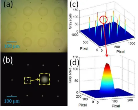
We took the pictures of the MLAs fabricated using 100-μm diameter shadow mask and measured the focus beam spot sizes by optical microscopy in Figure 2-6. It shows the uniform distribution of the intensity profile. Among the fabricated MLAs the average beam spot sizes were from 2.6 μm to 33.8 μm with variation less than 12%. The yield rate was higher than 96 %. We believe this can be further optimized in future. Figure 6 shows the scanning electronic microscopy (SEM) photograph of the microlenses using 100-μm diameter shadow mask under one minute UV/ozone treatment time. The cross section profile in Figure 2-7(e) indicates three layers, which are a glass substrate, a 5-μm thick SU-8 photoresist base layer, and an SU-8 photoresist microlens on the treated area. Two dimensional profiles of MLAs measured by surface profiler showed that the lenses had good surface smoothness. The surface roughness was less than 0.07 μm. This is a typical value for microlenses without going through etching process. We made the curve fitting of the microlens profile by using the SAG equation,
Table 2-1 The footprint diameters of MLAs.
Diameter of shadow mask (μm)
UV/ozone treatment time (minute)
one two three four
50 20 μm 30 μm 41.3 μm 41.6 μm
100 52 μm 80 μm 86 μm 95.5 μm
200 95 μm 164 μm 182 μm 192 μm
constant. From the fitting result, the conic constant was between -0.005 and 0.00036, which means the surface curvature of MLA fabricated by this method was spherical. We measured the wavefront information by using the commercial Shack-Hartmann wavefront sensor (UI2210-m, UEye, NL) to evaluate the optical quality. The corresponding peak-to-valley (PV) and root-mean-square (RMS) values were lower than 0.949 λ and 0.143 λ as shown in Figure 2-8. The experimental results were summarized in the Table 2-2 below. The yield rates were obtained by average of each 5 samples using the beam spot images. We believe this can be further optimized in future.
Figure 2-6 The MLAs fabricated using 100-μm diameter shadow mask. (a) Optical microscopy and (b) the corresponding focus points with (c) intensity profile for four minutes UV/ozone treatment time. (d) Zoomed image of the optical intensity profile.
Figure 2-8 The interferogram of the wavefront surface measurement. (a) 50 μm (b) 100 μm (c) 200 μm.
Figure 2-7 The SEM of (a) microlenses of 100 μm diameter under one minute UV/ozone treatment time. (b) the cross section profile of one minute treated microlens.
Table 2-2 The summarized results of fabricated MLAs.
Diameter (μm) UV/ozone time (minute)
Focal length (mm)
Beam Spot Size (μm)
Variation Yield Rate (%)
50
one 0.06 2.6 < 12% 96.5
two 0.11 4.7 < 11% 97.1
three 0.38 7.1 < 4% 98.7
four 0.39 7.1 < 4% 98.8
100
one 0.24 6.7 < 11% 96.7
two 0.65 8.9 < 9% 96.9
three 1.01 9.8 < 4% 97.1
four 1.35 10.78 < 3% 97.3
200
one 0.44 7.3 < 10% 96.9
two 1.24 10.2 < 10% 97.8
three 2.17 32.1 < 5% 97.5
four 2.78 33.8 < 2% 98.8
2.4 Conclusions
A transparent and self-assembled MLAs fabricated by use of the hydrophilic effect under UV/ozone treatment was presented and demonstrated experimentally. This method provides a fast, low cost, no etch-transfer, no lithography fabrication processes.
The MLA was made of negative photoresist SU-8 (n=1.63 @ 530 nm) on a glass substrate. The focal length of MLA is controllable by changing UV/ozone treatment time. A larger shadow mask opening and a longer UV/ozone treatment time produced MLA with longer focal length. MLAs of 50 μm, 100 μm, 200 μm diameters for one, two, three, and four minutes UV/ozone treatment time has been fabricated successfully. The numerical apertures of microlens were from 0.06 to 0.19. The focal lengths were from 0.06 mm to 2.78 mm. The surface roughness was less than 0.07 μm and the shape was nearly spherical. The yield rate was higher than 96 %. The corresponding PV and RMS values of wavefront were lower than 0.949 λ and 0.143 λ.
References
[1] H. Peng, Y. L. Ho, X.-J. Yu, M. Wong, and H.-S. Kwok, "Coupling efficiency enhancement in organic light-emitting devices using microlens array - Theory and experiment," IEEE/OSA Journal of Display Technology, vol. 1, pp. 278-282, 2005.
[2] J.-W. Pan, C.-M. Wang, H.-C. Lan, W.-S. Sun, and J.-Y. Chang, "Homogenized LED-illumination using microlens arrays for a pocket-sized projector," Optics Express, vol. 15, pp. 10483-10491, 2007.
[3] G. Y. Yoon, T. Jitsuno, M. Nakatsuka, and S. Nakai, "Shack Hartmann wave-front measurement with a large F-number plastic microlens array," Applied Optics, vol. 35, pp.
188-188, 1996.
[4] N. A. Davies, M. McCormick, and M. Brewin, "Design and analysis of an image transfer system using microlens arrays," Optical Engineering, vol. 33, pp. 3624-3633, 1994.
[5] S. Sinzinger and J. Jahns, Microoptics: Wiley-VCH, 1999.
[6] H. Ottevaere, R. Cox, H. P. Herzig, T. Miyashita, K. Naessens, M. Taghizadeh, R.
Volkel, H. Woo, and H. Thienpont, "Comparing glass and plastic refractive microlenses fabricated with different technologies," Journal of Optics A: Pure and Applied Optics, vol. 8, p. S407, 2006.
[7] H. A. Biebuyck and G. M. Whitesides, "Self-organization of organic liquids on patterned self-assembled monolayers of alkanethiolates on gold," Langmuir, vol. 10, pp.
2790-2793, 1994.
[8] D. M. Hartmann, O. Kibar, and S. G. Esener, "Characterization of a polymer microlens fabricated by use of the hydrophobic effect," Optics Letters, vol. 25, pp.
[9] O. P. Parida and N. Bhat, "Characterization of optical properties of SU-8 and fabrication of optical components," in Int. Conf. on Optics and Photonics, CSIO, Chandigarh, India, 2009.
[10] S.-M. Kuo and C.-H. Lin, "Fabrication of aspherical SU-8 microlens array utilizing novel stamping process and electro-static pulling method," Opt. Express, vol. 18, pp.
19114-19119, 2010.
[11] C.-J. Chang, C.-S. Yang, L.-H. Lan, P.-C. Wang, and F.-G. Tseng, "Fabrication of a SU-8-based polymer-enclosed channel with a penetrating UV/ozone-modified interior surface for electrokinetic separation of proteins," Journal of Micromechanics and
Microengineering, vol. 20, 2010.
[12] K. Oura, Surface science: an introduction: Springer, 2003.
Chapter 3 Fabrication of Transparent and Self-Assembled Microlens Array Using Hydrophilic Effect and Electric Fielding Pulling
In this work, we present a variable and self-assembled spherical microlens array (MLA) fabricated by the use of the hydrophilic effect under ultra-violet (UV)/ozone treatment. The optical power and surface roughness of MLA was further enhanced by applying external electric field. This method provides a fast, simple, and low cost process, because it does not require heating, or etch-transfer processes. The MLA was made of negative photoresist SU-8 (n = 1.63) on a glass substrate. Microlenses from 50 μm to 200 μm diameters with one, two, three, and four minutes UV/ozone treatment time were successfully fabricated. The optical focusing power of 100-μm diameter MLA was also improved by using electric field of 1.7 V/μm, and 3.4 V/μm. A 10-μm thick shadow mask was used to define the UV/ozone treatment area to create more hydrophilic surfaces on an SU-8 photoresist base layer on a glass substrate. After hydrophilic zones were created, the glass substrate was immersed into a diluted SU-8 photoresist solution and then removed. Finally, the MLA was formed after applying parallel electric field followed by UV curing process. The MLA was kept in spherical shape while the radius of curvature was changed. The focal length from 0.09 mm to 2.91 mm of spherical MLA were experimentally demonstrated and investigated.
3.1 Introduction
Micro-lens array (MLA) is an important component which is used widely in many applications, such as increasing the light extraction efficiency [1], Shack Hartmann wavefront sensor [2], beam shaping for illumination [3], light gathering for solar collectors [4], and information displays [5]. There have been many techniques to fabricate micro-lens array, including thermal reflow [6], UV resin stamping [7], laser ablation [8], ink-jet printing [9], direct laser writing [10], and gray-scale mask photolithography [11] methods. Most of these mentioned methods have the drawbacks of high facility cost, time consumption, alignment inaccuracy, or high temperature process. The main problem of the high temperature process in some of these methods is inducing device defects in several applications, such as backlight module of liquid crystal display (LCD) and the encapsulation of light emitting diode (LED). There is another approach to fabricate MLAs by the use of hydrophobic effect [12, 13]. This approach allows accurate and direct fabrication of polymer microlens array without heating. Thus, using the hydrophobic effect to fabricate MLAs is a simpler way.
However, it still requires either an etch-transfer process or lithography to define hydrophobic boundaries, which increases the cost and process complexity. Therefore, a cost effective and low temperature process is still desirable to fabricate MLAs.
SU-8 photoresist (MicroChem, MA) has high optical transmittance from visible to near-infrared wavelength and high refractive index (~1.63) [14]. Furthermore, it has better chemical resistance and mechanical strength than other popular polymers, such as polycarbonate or poly-methyl-methacrylate (PMMA). As a result, SU-8 photoresist is
footprint of SU-8 photoresist liquid droplet was fixed on a substrate and the center part, or sag height, was pulled up. This made a higher sag height and a corresponding larger optical power [16].
In this work, a transparent and self-assembled MLA in spherical shape was fabricated by the use of hydrophilic effect and external electric field pulling. A base layer of SU-8 photoresist can be surface modified to become more hydrophilic using ultra-violet (UV)/ozone cleaner [17]. The MLA was made of diluted SU-8 photoresist on the SU-8 photoresist base layer. It was self-assembled by the balance of surface tension energy on the SU-8 photoresist base layer of more-hydrophilic circular zones. In some applications, a larger optical power MLA is desirable. Therefore, an external electric field was applied to increase the optical power and to smooth the surface roughness before UV curing of SU-8 photoresist. The presented method provides a fast, low cost, and no etch-transfer process. The entire fabrication was done in room temperature to prevent it from thermal residual stress and material issues. The radius of curvature of the microlens can be easily controlled by the design of shadow mask opening, the UV/ozone treatment time, and the external electric field. In the following sections, the working principle and fabrication process are discussed. This work investigates the focal length of MLA under different lens diameters, the UV/ozone treatment time and the electric field strength. Experimental results of optical microscopy images, focus spot diagrams, lens profiles, surface roughness, and scanning electric microscope (SEM) images of the fabricated MLA were presented in this work.
3.2 The working mechanism
substrate with an SU-8 photoresist base layer. SU-8 is a well-known photoresist which has good mechanical strength and UV curable property. The surface can be modified to be more hydrophilic by using UV/ozone treatment. It generates O−H on the phenol group, C=O and O−C=O hydrophilic function on SU-8 photoresist surfaces. This contributes to the hydrophilic surface of SU-8 polymer. The contact angle on the modified surface depends on the processing time, UV power and ozone concentration.
The polar molecules enable SU-8 photoresist structures to be easily deformed by an external applied electric field. The larger electric field results in a higher sag height of the microlens. The SU-8 photoresist base layer keeps the microlens as a spherical profile via an external electric field. The base layer is served as a dielectric middle layer between SU-8 microlens and ITO conductive layer. Figure 3-1 illustrates schematically the working principle of SU-8 photoresist MLA by the use of the hydrophilic effect through UV/ozone treatment and the external electric field pulling. A 10-μm thick SU-8 photoresist shadow mask with circular openings was used to define the UV/ozone treatment areas on the SU-8 photoresist base layer, as in Figure 3-1(a). The exposed zones became more hydrophilic than the obstructed zones after UV/ozone treatment, as in Figure 3-1(b). According to the surface modification, more treatment time results more hydrophilic surfaces. In other words, a smaller contact angle was formed under longer UV/ozone treatment time. After the more hydrophilic zones were created and the SU-8 photoresist mask was removed, the substrate was dipped in and out of the diluted SU-8 photoresist solution with a slow and constant velocity (approximately 0.3 mm/sec), as in Figure 3-1(c). Finally, SU-8 photoresist MLA was formed on the substrate after
concentration of diluted SU-8 photoresist must be diluted to automatically stay on the areas with more hydrophilic property. Because of the evaporation of the solvent after UV curing process, the volume of the diluted SU-8 photoresist liquid microlens shrank.
Therefore, the contact angle was smaller compared with the default one and the footprint area was smaller than the shadow mask opening. In general, a higher surface energy of SU-8 base layer results in a larger footprint area. In the other words, longer UV/ozone treatment time and larger shadow mask opening result in higher surface energy
. On the other hand, the external electric field reduces the surface energy of SU-8
base layer. It increases the contact angles of SU-8 microlens, which decreases the radius of curvature and keeps the spherical profile. In these regards, the shape and the size can be manipulated by controlling the UV/ozone treatment time, the shadow mask opening, and the external applied voltage for this process.3.3 Fabrication processes
In order to define the hydrophilic zones, we fabricated an SU-8 photoresist shadow mask at first. The SU-8 photoresist shadow mask has good mechanical strength and chemical resistance; therefore, it is removable and reusable. It was fabricated by micromachining processes. First, the SU-8 photoresist was spun on the glass substrate with the speed of 500 rpm for 5 sec and 1000 rpm for 30 sec. Then, it was soft baked at 95 ℃ for 3 min followed by 3.2 J/cm2 exposure in the wavelength of 405 μm with
Figure 3-1 The schematic of the presented fabrication of the SU-8 MLA.(a)
UV/ozone treatment (b) Hydrophilic zones is presented (c) Dip out from the diluted SU-8 photoresist solution (d) Apply the external voltage.
The SU-8 photoresist shadow mask with circular openings was released by isotropic etching in buffered oxide etcher (BOE). The thickness of shadow mask was approximately 10 μm.
In this study, ITO glass (LT-G001, Lumtek Corp., Taiwan) with 1.1 mm of glass thickness and 1600 Å of ITO thickness was cut into pieces with a dimension of 25 mm and 25 mm. It was used as the substrate. The ITO resistance was 15 Ω/sq and the transparency of ITO was larger than 84% at wavelength of 550 nm. A commercially available SU-8 3035 negative photoresist, an SU-8 2000 thinner, and an SU-8 developer were used in this fabrication (MicroChem Corp., MA, USA). For cleaning the substrate, the ITO glass was first cleaned with acetone, isopropanol alcohol (IPA) and deionized (DI) water, and then dehydrated on a hot plate with a temperature of 100 ℃ for 10 min.
Figure 3-2 shows schematic drawings of the fabrication process of the presented method.
The detailed fabrication processes are described below.
3.3.1 SU-8 photoresist base layer
In this work, we chose ITO glass as a substrate because its hydrophilic surface produces a flatter coating of SU-8 photoresist and the ITO was served as a conductive layer. We employed the spin coating method (NMC-W-1102, Laurell Technologies Corp., USA) to coat SU-8 photoresist on the ITO glass. The spin speed was 500 rpm for 5 sec and 4000 rpm for 30 sec. In order to produce a thinner SU-8 photoresist layer, the weight ratio of it was a 10:8 mixture of SU-8 3035 and SU-8 2000 thinner. The baking process was skipped in order to control the process at room temperature. It was finally exposed to 9.6 J/cm2 of UV curing. An SU-8 photoresist base layer with 5 μm thickness
![Figure 1-11 Lens like phase retardation when applying voltage on LC cell. [14] (a) No voltage apply](https://thumb-ap.123doks.com/thumbv2/9libinfo/9599404.628652/30.892.184.711.470.656/figure-lens-phase-retardation-applying-voltage-voltage-apply.webp)