碩士論文
Department of Physics College of Science
National Taiwan University Master Thesis
層狀材料中的傳輸性質
Transport Properties of Some Layer Compounds
孔祥曦
Hsiang-Hsi Kung
指導教授﹕郭光宇 李偉立 博士
Advisor: Guang-Yu Guo, Wei-Li Lee, Ph.D.
中華民國 100 年 8 月
August, 2011
口試委員會審定書
層狀材料中的傳輸性質
Transport Properties of Some Layer Compounds
本論文條、孔祥曦君 (R98222075 )在國立臺灣大學物理學系、
所完成之碩/博士學位論文,於民國 100 年 7 月 29 日承下列考試委員
審查通過及口試及格,特此證明
口試委員:
字~說
(簽名)三
♂去 才.t~…導翱枷教掀授
A7紳 草弘
I would like to thank my adviser Wei-Li Lee for his mentorship and support. He is always passionate and generous in sharing his knowledge of science and life. I have benefited tremendously from the discussions with him. His enthusiasm and attitude regarding re- search will serve as a model for me.
I am also grateful to Professor Guo for the discussions we had and his kind advice on improving my thesis. I wish to give special thank to Professor Chou and Dr. Sankar for providing me high quality crystals.
I have benefited greatly from other members in the group. I am particularly indebted to Vincent Lu who kindly shared his knowledge and experiences in transport measurements with me. Chang-Ran Wang, Chris Chen, and Feng Lin shared their valuable experiences in micro-sized device fabrication with me. The discussions with Chi-Chih Ho had always been delightful and helpful. Chia-Tso Hsieh, Chih-Ping Lu, and Ting-Hui Chen are won- derful lab-mates and friends. I am also thankful to the technical staffs in the clean room for their guidance and help with my experiments.
Finally, I want to thank my family and friends for their endless support and under- standing. Their encouragements have provided me with unbelievable strength through out these years.
i
中文摘要
在過去的十年中,準低維度系統(quasi-low-dimensional systems)在凝態物理內 吸引了很多的注意。在這篇論文中,我們針對兩個特定的系統進行討論:拓撲絕 緣體(topological insulator)和雙晶格不匹配化合物(misfit compound)。拓撲絕緣體 的費米面(Fermi surface)位在一個能隙(band-gap)之中,因此本身是絕緣體。但 是在這個能隙中,還有一組連續的表面能態(surface states),其中電子的有效質量 為零並且自旋極化。表面能態中電子被限制在樣品表面流動,因此為研究準低維 度系統中的傳輸性質提供了一個很好的舞台。由於受到時間反演對稱性(time reversal symmetry)的保護,拓撲絕緣體中的表面能態不會被非磁性雜質和缺陷所 破壞。根據理論的預測,表面狀態上有著許多不尋常的傳輸特性,可能在自旋電 子學(Spintronics)和量子計算(quantum computing)上有很多的應用。雖然表面狀 態可以被角分辨光電子能譜(Angle Resolved Photoemission Spectroscopy, ARPES)所 看到,從傳輸量測上要分辨表面能態仍然充滿挑戰。這主要是因為很大一部分的 訊號來自於塊材電子能帶(bulk electron band),淹沒了來自於表面能態的訊號。在 這篇論文中,我們將分析Bi2Se3在單晶和微電子元件(micro-sized device)中的傳輸 訊號,並專注於表面能態的鑑定。我們在大磁場下看到明顯的量子震盪(quantum oscillations),它提供了一種識別費米面形狀的方法。由振盪頻率和磁場角度的關係 我們推斷訊號主要來自於一個三維的費米面。這表示,電導率主要來自於塊材的 電子能帶。我們在Bi2Se3上的研究經驗,將來可以輕易地應用在其他新的拓撲絕緣 體表面能態的鑑定上。
準低維度系統中,另外一個有趣的研究對象的是雙晶格不匹配化合物。在這
ii
些晶體中,兩種不同晶格常數的層狀化合物互相堆疊,使得整體晶格結構「不匹 配」。由於相鄰原子層之間僅靠著凡得瓦力(van-der-Waals force)鍵結,這些化合 物也可以被視為一種準低維度系統。其中一個特別有趣的系統,是由電荷密度波
(charge density wave, CDW)材料與另外一種材料(通常是半導體)所構成的雙晶 格不匹配化合物。這兩種化合物個別都不具有超導性質(superconductivity)。我們 發現,他們所構成的雙晶格不匹配化合物在低溫下卻具有超導電性。此外,相鄰 原子層之間的電荷轉移(charge transfer)和應力使得這個系統更加複雜和耐人尋 味。一般認為,電荷轉移能抑制電荷密度波的形成,並且誘發超導電性。雙晶格 不匹配化合物超導體為這個議題提供了一個研究平台。我們將提供幾個分別屬於 1T-TaS2和1T-TiSe2系統中,雙晶格不匹配化合物超導體傳輸性質的數據。我們觀察 到電荷轉移與電荷密度波抑制的證據。我們的分析顯示,電荷密度波和超導電性 之間有著互相競爭的關係。研究更多類似的樣品將有助於確認這種競爭關係。
For the past decade, a lot of attention in condensed matter physics had been focused on quasi-low-dimensional systems, which compose the main structure of this thesis. Two particular systems are discussed: topological insulators and superconductivity in misfit compounds. Topological insulators are materials with a bulk insulating band-gap, tra- versed by gapless surface conduction channels that carry massless spin polarized elec- trons. The electrons in surface states are confined to propagate on sample surface provid- ing a good stage for studying electron transport in quasi-low-dimensional system. Such surface states are protected against non-magnetic impurities and defects due to time re- versal symmetry. The surface states are predicted to exhibit various unusual transport properties that may promise applications in spintronics and quantum computing. Al- though surface states has been demonstrated by Angle Resolved Photoemission Spec- troscopy(ARPES), it remains challenging from transport measurements. This is mostly due to the fact that electrons in bulk bands also contribute significantly to the charge transport, and signals due to surface states are therefore overwhelmed. In this thesis, we will focus on the identification of surface states. Transport data on bulk Bi2Se3 and micro-sized Bi2Se3 will be presented and discussed. We observed Shubnikov-de Hass oscillations at large magnetic field which provides a way to identify the dimensionality of Fermi surface. Our observed oscillation frequency’s angular dependence infers a 3D Fermi surface. This indicates that the conductance is still dominated by bulk band. Our experimental setup and experiences on Bi2Se3can be used on other topological insulators
iv
in the future.
Another interesting system for the study of quasi-low-dimensional system is the misfit compounds. Misfit compounds are alternating stacks of two layer compounds with dif- ferent lattice constants. The non-coincidence of periodicity between neighbouring layers causes the mismatch of crystal structure in certain direction, making the overall crystal structure “misfit”. Since the adjacent layers are usually weakly bound by van-der-Waals force, the misfit compounds can also be viewed as a quasi-low-dimensional system. An interesting issue is the intercalation of a charge density wave (CDW) material with an- other compound (typically a semiconductor). Both compounds are non-superconducting separately. We found that the resulting misfit compound sometimes turns out to be con- ductive and superconducting. In addition, the effect of charge transfer between adjacent layers and stress between misfit layers, further makes the system more complicated but also intriguing. It was usually believed that charge transfer can suppress CDW ordering and induce superconductivity. Misfit superconductors provides a platform for studying the competition between CDW and superconductivity. I will present our transport data on several misfit superconductors belong to 1T-TaS2 and 1T-TiSe2 family. We observed evidence of charge transfer and CDW suppression in those misfit superconductors. Our data implies that CDW is competing with superconductivity at low temperature. Detailed study on samples with different intercalation will help to illustrate the competition be- tween CDW and superconductivity.
Acknowledgement i
ii
Abstract iv
Contents vi
List Of Figures viii
List Of Tables xii
1 Introduction 1
1.1 Topological Insulator . . . 1
1.2 Identification of Surface States . . . 8
1.3 Superconductivity in Misfit Compounds . . . 12
2 Experimental Setup 16 2.1 Superconducting Magnet System . . . 16
2.2 Electromagnet System . . . 17
2.3 Thin Film Deposition System . . . 20
2.4 Sample Preparation . . . 21
2.4.1 Bulk Single crystals . . . 21
2.4.2 Micro-sized Devices . . . 24
vi
中文摘要
3 Experimental Results 28
3.1 Bulk Bi2Se3 Single Crystals . . . 28
3.2 Micro-sized Bi2Se3Devices . . . 41
3.3 Superconductivity in Misfit Compounds . . . 45
3.3.1 1T-TaS2System . . . 45
3.3.2 1T-TiSe2System . . . 53
4 Discussion 56 4.1 Surface States Identification in Topological Insulators . . . 56
4.2 Competition Between CDW and Superconductivity in Misfit Supercon- ductors . . . 65
5 Conclusion 69
References 71
1.1 Typical band structure of a trivial insulator and a topological insulator. . . 3 1.2 Bi2Se3 surface state based on first principle calculation [1] and ARPES
result [2]. . . 4 1.3 The crystal structure of Bi2Se3 (from Ref. [1]). . . 5 1.4 Schematic drawing and ARPES result of Bi2Se3surface state spin texture
near Fermi surface. . . 7 1.5 (a)Schematic of the interference paths in AB effect experiment and their
expected interference periods. (b)Experimental result of AB interference in Bi2Se3 nano-ribbon from Ref. [3]. . . 9 1.6 Identification of surface states in non-metallic Bi2Te3, data from Ref. [4].
(a)The resistivity derivative dρxx/dH versus inverse perpendicular field.
(b)Field position of the resistivity minima corresponding to ν = 3 Landau level plotted against field angle. (c)Hall conductivity versus magnetic field. (d)Surface and bulk term of Hall conductivity separated from (c). . . 11 1.7 (a)Schematic drawing of the structure of a typical misfit compound. (b)The
structure of a typical MX compound. (c)An example of how the superpo- sition of the host compounds’ electron D.O.S. explains charge transfer. . . 15 1.8 (a)Schematic of how the collective behaviour of CDW results in a net cur-
rent when electric field is applied. (b)Schematic of how the atom positions and electron density are modulated in CDW. Pictures from Ref. [5]. . . . 15
viii
2.1 Schematic of superconducting magnet system and side view of probe sample space. . . 18 2.2 Schematic of electromagnet system and side view of sample holder. . . . 19 2.3 Photos showing how bulk single crystals are connected to superconduct-
ing magnet sample probe. . . 22 2.4 Schematic of the model and parameters used for Bi2Se3OM contrast sim-
ulation. . . 25 2.5 (a)Simulation and (b)experimental data of Bi2Se3 OM contrast with re-
spect to sample thickness on 300nm SiO2 wafer under green light illumi- nation. . . 25 2.6 Schematic of how bottom gate voltage is applied upon micro-sized crystal
samples. . . 27
3.1 A typical RT plot for a metallic Bi2Se3 single crystal. . . 29 3.2 ρyxplot against magnetic field for different batch of Bi2Se3. . . 31 3.3 Hall resistivity ρyxof bulk Bi2Se3versus field at various angles on a plane
perpendicular to current. . . 32 3.4 MR of bulk Bi2Se3 plot against magnetic field for different batch of Bi2Se3. 33 3.5 MR of bulk Bi2Se3 versus field at various angles tilt from c-axis on the
plane perpendicular to current flow. . . 34 3.6 MR of bulk Bi2Se3 versus field at various angles tilt from c-axis on the
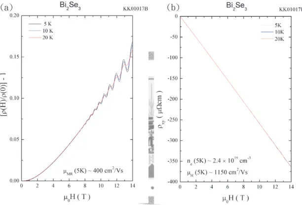
plane parallel to current flow. . . 35 3.7 (a)MR of bulk Bi2Se3 (KK01017B) measured at various temperatures
with out-of-plane magnetic field. (b)Hall resistivity of bulk Bi2Se3 mea- sured at various temperatures with out-of-plane magnetic field. . . 36 3.8 (a)MR of bulk Bi2Se3 (RS-210-B1) measured at various temperatures
with out-of-plane magnetic field. (b)Hall resistivity of bulk Bi2Se3 mea- sured at various temperatures with out-of-plane magnetic field. . . 37
3.9 Resistivity plot against temperature from 2K to 300K for CaxBi2Se3 with different x. . . . 38 3.10 (a)MR and (b)Hall effect of Ca doped Bi2Se3measured at 2K. . . 39 3.11 (a)Hall resistivity and (b)MR plot against magnetic field for different x in
Bi2Se3+x. (c)Comparison of the carrier concentration and Hall mobility of Bi2Se3+x, with x raging from 0 to 0.2. . . . 40 3.12 Resistivity plot against temperature from 5K to 300K for Bi2Te2Se. . . . 42 3.13 (a)MR and (b)Hall effect of Bi2Te2Se measured at 5K. . . 43 3.14 (a)The RT curve of a micro-sized Bi2Se3 with the application of top gate
voltage. (b)The OM image of the device in (a). (c)The AFM images of the Bi2Se3 crystal in (a). . . 45 3.15 The MR plot against magnetic field under different top gate voltage at 5K
for a micro-sized Bi2Se3device. . . 46 3.16 The normalized resistivity with respect to top gate voltage at (a) 0 and (b)
14 Tesla for a micro-sized Bi2Se3 device. . . 47 3.17 The resistivity versus bottom gate voltage for a micro-sized Bi2Se3 device. 48 3.18 The RT curve of (SnS)(TaS2). . . 49 3.19 (a)MR and (b)Hall resistivity of (SnS)(TaS2) plot against magnetic field. . 49 3.20 The RT curve of (SnS)(TaS2) near Tcat different (a)currents and (b)magnetic
fields. . . 50 3.21 The RT curve of (SnS)(TaS2)2 and 1T-TaS2. . . 51 3.22 (a)MR and (b)Hall resistivity of (SnS)(TaS2)2 plot against magnetic field. 52 3.23 The RT curve of (SnS)(TaS2)2near Tcat different (a)currents and (b)magnetic
fields. . . 52 3.24 The RT curve of the misfit compound (PbSe)(TiSe2)2. . . 54 3.25 (a)MR and (b)Hall resistivity of (PbSe)(TiSe2)2 plot against magnetic field. 55
3.26 The RT curve of (PbSe)(TiSe2)2near Tcmeasured with different (a)currents and (b)magnetic fields. . . 55
4.1 Resistivity derivative dρxx/dH of Bi2Se3 versus inverse field at various angles on the plane perpendicular to current. The inset shows FFT ampli- tude vs. frequency. . . 58 4.2 The SdH oscillation frequency of bulk Bi2Se3 plot against field angle
(open circle). . . 59 4.3 (a)The extremal cross-sectional area (Ae) of an ellipsoidal Fermi surface
at 0 and 90◦. (b)Ae of a 2D Fermi surface at 0◦. (c)Ae of a 2D Fermi surface at 50◦. . . 59 4.4 Hall resistivity derivative dρyx/dH of bulk Bi2Se3 versus inverse field at
θ = 0. The inset is its FFT spectrum. . . . 60 4.5 △ρxxof bulk Bi2Se3plot against inverse field at three different temperatures. 62 4.6 The (a)temperature and (b)field dependence of the SdH oscillation ampli-
tude for bulk Bi2Se3. . . 63 4.7 The resistivity derivative of micro-sized Bi2Se3 plot against inverse field
without top gate voltage. . . 64 4.8 The resistivity derivative of micro-sized Bi2Se3 plot against inverse field
with (a)Vtg=-20V and (b)Vtg=+20V. . . 65 4.9 Jc plots against the normalized Tc (open circles) for (a)(SnS)(TaS2) and
(b)(SnS)(TaS2)2. . . 67 4.10 Hc plot against the normalized Tc (open circles) for (a)(SnS)(TaS2) and
(b)(SnS)(TaS2)2. . . 67 4.11 Hcplot against the normalized Tc(open circles) for (PbSe)(TiSe2)2. . . . 68
2.1 A list of the batch numbers and growing methods of the topological insu- lator crystals presented in this thesis. . . 23 2.2 A list of the batch numbers and growing methods of the misfit compounds
presented in this thesis. . . 24
3.1 Some basic properties obtained from transport measurements on different batches of Bi2Se3. . . 30
xii
Introduction
1.1 Topological Insulator
Insulators are known as materials with a large band gap between occupied and empty bands (Fig. 1.1a). 3D Topological insulators are similar to trivial insulators in the sense that their Fermi surfaces are both within bulk band gap. But in the case of topological in- sulator, there are additional gapless surface states inside the bulk band gap (Fig. 1.1b) that intersect at the ”Dirac point”. These additional states support 2D conducting channels at the surface, and are protected from non-magnetic impurity scatterings due to time reversal symmetry. The energy dispersion of the surface states is linear with the wave-vector k, E = vF¯hk, where vF is Fermi velocity. Due to it’s linear dispersion, the effective mass m∗ ∝ d2E/dk2 of Dirac Fermion near Dirac point is zero. Their wavefunction must be described by Dirac equation rather than Schr¨odinger equation. The charge carriers in the surface states are also called ”Dirac fermions”. One direct consequence of zero effective mass is the well defined chirality
h≡ σ·p = ±1, (1.1)
where σ is Pauli matrix and p is momentum unit vector. For typical particles with non- zero mass, p depends on the observer’s reference frame and may even change sign if the
1
observer is moving faster than the particle. Therefore, chirality is not well-defined for massive particles. But the eigenvalue of chirality operator is irrelevant to the observer’s reference frame when acting on wavefunctions described by Dirac equation. Therefore, the chirality of Dirac fermion is well-defined and the surface states are referred to as
“chiral states”. A consequence of well-defined chirality is the suppression of the 2kF- scatterings (backscattering). Since chirality is a conserved physical quantity in topologi- cal insulators, electrons moving in opposite direction are required to have opposite spins (from Eq 1.1). Therefore, backscattering is suppressed since it requires higher energy to flip electron spins. Another consequence of the linear dispersion is the π-shift in Berry’s phase, γ [6]. We know that electrons in crystals moving in a closed trajectory at con- stant energy in momentum space gains an additional phase called Berry’s phase which is zero in typical conductors and π in massless Dirac materials (without considering spin- orbit coupling). Further consideration of spin-orbit interaction (which is non-negligible in topological insulators) will modify this π shift in Berry’s phase [7]. The exact value of this phase shift can be experimentally determined through Shubnikov-de Hass oscillations (to be discussed below).
Bi1−xSbx, Bi2Se3 and Bi2Te3 were first theoretically predicted to be 3D topological insulators [8, 1]. Later on, the 2D surface state of Bi1−xSbxwas experimentally confirmed using Angle Resolved Photoemission Spectroscopy (ARPES) [9]. Soon after, Bi2Se3[2]
and Bi2Te3 [10] were also experimentally confirmed by ARPES. Calculated band struc- ture of Bi2Se3 is shown in Fig. 1.2a, the warmer color denotes a higher density of states (D.O.S.). The gapless states with linear dispersion can be seen crossing bulk band-gap.
The center white line denote the position of Fermi surface. Experimental result of Bi2Se3 from ARPES is shown in Fig. 1.2b. The color code denotes ARPES spectra height, which is proportional to electron D.O.S. The yellow areas are bands with high D.O.S., indicating the position of bulk bands, the lower one and upper one are valence band and conduction band, respectively. The white dotted line marks the position of the Fermi level. A red
Energy
E F E
g>>k
BT k
Energy
E F
k
)b* )c*
Wbmfodf Cboe
Dpoevdujpo Cboe
Wbmfodf Cboe
Dpoevdujpo Cboe
Usjwjbm!Jotvmbups Upqpmphjdbm!Jotvmbups
Figure 1.1: (a)Typical band structure of a trivial insulator. Colored area denote bands filled by electrons. Valence band is totally filled while the conduction band is empty.
They are separated by a band gap Eg, which is much larger than the thermal energy kBT . The dash line depicts the position of Fermi level EF. (b)The band structure of an ideal topological insulator. The gapless surface states are denoted by the red lines. The band gap size is typically about 300 meV, which is similar to semiconductors.
colored, gapless band with almost linear dispersion can be seen inside the bulk band gap.
The electron cyclotron mass can be estimated from the energy dispersion in Fig. 1.2b.
The cyclotron effective mass is usually defined by [11]
mc = ¯h2 2π
∂A
∂E, (1.2)
where A is k-space area enclosed by the orbit and E is the energy. Combine the above equation with the linear dispersion relation of Dirac fermions, E = vF¯hk, it can be shown that mc= ¯hk/vF. Therefore, the cyclotron mass is zero at Dirac point. The Fermi velocity estimated from Fig. 1.2b is∼ 4.6 × 10⁵m/s, and the cyclotron mass in surface states near EF is ∼ 0.25m0 (kF ∼ 0.1 ˚A−1 and EF ∼ 300meV ), where m0 is the free electron mass. For the electrons in the bottom of conduction band in Fig. 1.2b (assume parabolic dispersion, E = ¯h2k2/2mc), the estimated cyclotron mass mc ∼ 0.12m0 for electrons near EF (kF ∼ 0.04 ˚A−1and EF ∼ 50meV ).
The crystal structure of Bi2Se3 is shown in Fig. 1.3 (figure from Ref. [1]). The prim- itive lattice vectors are denoted as t1, t2, and t3. It has layered structure with a triangular lattice within one layer. Each unit cell consists of five-atom layers along the c-axis, which
)b* )c*
Figure 1.2: Bi2Se3 electronic band structure. (a)Theoretical work based on first princi- ple calculations from Ref. [1]. The warmer color indicate higher electron D.O.S., the blue regions are bulk band-gap. The upper and lower irregular red region are the bulk conduc- tion and valence band, respectively. A linear dispersed gapless surface state can be seen inside the bulk band-gap. (b)The ARPES measurement of surface electronic band struc- ture from Ref. [2]. The warmer color denotes higher electron D.O.S., the black region is bulk band-gap. The upper and lower yellow regions are bulk conduction and valence band, respectively. The white dash line marks the position of Fermi level. A red colored, gapless band with nearly linear dispersion can be seen inside the bulk band gap.
)b* )c*
)d*
Figure 1.3: The crystal structure of Bi2Se3 (from Ref. [1]) (a)Crystal structure with three primitive lattice vectors denoted as t1, t2, and t3. A quintuple layer is indicated by the red square. (b)Top view along the z-direction. The lattice atoms in a quintuple layer have three different positions, denoted as A, B, and C. (c)Side view of the quintuple layer, which is about 1nm thick.
is known as a quintuple layer (indicated by the red square). The lattice atoms in a quin- tuple layer have three different positions, denoted as A, B, and C. The thickness of each quintuple layer is about 1nm, and the coupling force between quintuple layers is weak (van-der-Waals type).
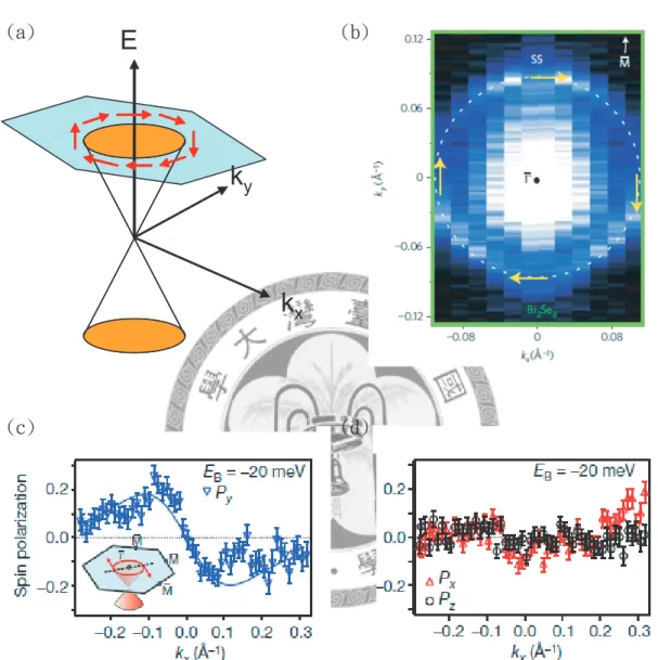
One of the most important feature of the surface state is it’s spin texture. The electron spins of the surface states are predicted to be in-plane and perpendicular to the momen- tum (see Fig. 1.4a). The red arrows denote spin direction of each point on the intersection of Fermi surface and Dirac cone. Those spin textures have been verified by ARPES (Fig. 1.4b-d). Figure 1.4b is the top view of the Dirac cone intersection with Fermi sur- face, the yellow arrows are the expected spin orientation. The inner white area is the bottom of bulk conduction band, but a darker ring with radius∼0.1 ˚A−1is the intersection of Dirac cone with Fermi level. Figure 1.4(c)and (d) show the measured spin polariza-
tions along the kx direction (z direction is defined as out of plane). No clear signal can be seen in x and z components. But in the y component, a clear peak of opposite sign and equal value at kx ∼ ±0.1 ˚A−1 can be seen, which is in accord with the position of Dirac cone edge. This observation agrees well with the theoretical prediction [12]. We can understate this spin texture in a simple way. We know that, due to relativistic ef- fect, moving charge carriers in their rest frame will experience an effective magnetic field Bef f∝vF×E, where vF is Fermi velocity of the charge carriers, and E is the electric field exerted on the charge carriers in crystal’s rest frame. This effect is more pronounced in systems with strong spin-orbit coupling. When considering the carriers confined on the surface of a crystal, those carriers will only experience an effective electric field Esalong out-of-plane direction from symmetry argument. Therefore, the effective magnetic field will be pointing along in-plane direction and perpendicular to vF. Electrons moving on the surface will then tend to line up their spins with Bef f in order to minimize Zeeman energy, which is proportional to σ·Bef f. From this point of view, charge carriers moving in opposite direction will have their spin polarization inverted. Because the effective field is pointing along opposite direction on the opposite surface, spin polarization of charge carriers moving in same direction but on opposite surface will also be inverted.
One might ask why are there so few topological insulators. Kane and Mele developed an easy way to distinguish non-trivial topological insulators (such as Bi2Se3) from trivial ones (band insulator) using a special topological invariant, Z2 [14, 15, 8]. They found that for a material with Fermi level inside band-gap, Z2 can only be 0 (trivial insulator) or 1 (non-trivial topological insulator). Z2 can be easily determined by counting number of Dirac pairs inside the band-gap and then take modulo 2. For materials with Z2=1, the gapless surface states are protected from weak disorder and non-magnetic impurities by time reversal symmetry (TRS). For materials with Z2=0, the surface states can be easily destroyed by a small perturbation and become trivial insulators.
)b*
E
)c*k
yk
x)d* )e*
Figure 1.4: (a) Schematic drawing of Bi2Se3 surface state spin texture near Fermi energy (denoted by the blue hexagon). The red arrows denote spin direction of each point on the intersection of Fermi surface and Dirac cone. (b)ARPES result from Ref. [2]. The inner white area is the bottom of bulk conduction band. A darker ring with radius ∼0.1 ˚A−1 is the intersection of Dirac cone with Fermi surface. The yellow arrows denote the spin directions. (c)-(d) are the spin polarizations along kx (z direction being defined as out of plane) ( results from Ref. [13]). No clear signal can be seen in x and z component. But in the y component, a clear peak of opposite sign and equal value at kx ∼ ±0.1 ˚A−1 can be seen, which is in accord with the position of Dirac cone edge.
1.2 Identification of Surface States
Although the surface states of topological insulators had been identified by ARPES mea- surements as mentioned in the previous section, verification from transport measurements are relatively few. The main reason is that Fermi surface is usually not in the bulk band gap, as it should be in an ideal case. Due to crystal growth difficulties, Fermi surface of Bi2Se3is typically in the bulk conduction band. Since the surface states’ D.O.S. is much smaller than the bulk band, the signal contribution from surface states are easily over- whelmed by the bulk bands. Therefore, the identification of surface states becomes tricky.
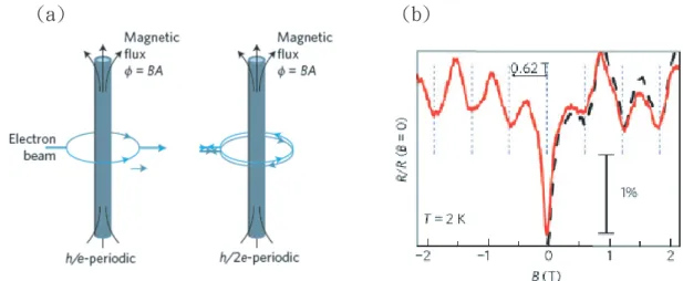
However, several methods had been used successfully to identify surface states from trans- port measurement. One is by Aharonov-Bohm interference (AB effect) [3, 16, 17]. Based on quantum mechanics, two electrons moving in a path enclosing nonzero magnetic flux ϕ (see Fig. 1.5a) will acquire a relative phase. There are two possible interference paths.
One is from the interference between two split electron beams as shown in the left picture of Fig. 1.5. Enclosed magnetic flux will cause alternating destructive and constructive in- terference with respect to the increasing magnetic field. The period of interference equals h/e, where h is Plank’s constant and e is the electron charge. The other one is the inter-
ference with it’s own time-reversed path. The conductance will oscillate with period of h/2e [18]. Since backscattering is suppressed in Dirac surface states, h/2e period is also
suppressed. As a result, the resistivity along the magnetic field direction should be oscil- lating with period h/e. This effect cannot be seen in normal metal wires due to the arbitrary in electron paths. However, the only conducting channel in topological insulators is the gapless surface state. Therefore, we expect to see the resistivity oscillation with respect to field strength at a constant period h/eA, where A is the sample’s cross-section area per- pendicular to field direction. This method was first demonstrated on Bi2Se3 nano-ribbon to reveal the Dirac surface states [3] (Fig 1.5b). The normalized magnetoresistance is plotted against magnetic field in the ribbon’s longitudinal direction at 2K. The resistivity
)b* )c*
Figure 1.5: (a)Schematic of the interference paths in AB effect experiment and their ex- pected interference periods. (b)Experimental result of AB interference in Bi2Se3 nano- ribbon from Ref. [3]. The resistivity is oscillating with a period of 0.62T, which corre- sponds to h/e period.
is oscillating with a period of 0.62T, which corresponds to h/e period. The drawback of probing surface states through AB effect is that it can only work in nanowire systems, and it requires large surface-to-volume ratio. According to Ref. [3], the cross-section needs to be smaller than 104 nm2 in order to see the effect. The geometrical limitations make this method less favorable.
Another way to identify surface states is through Shubnikov-de Haas (SdH) oscil- lations. Under magnetic field, electrons will undergo cyclotron motion, and their energy band will transform into discrete Landau levels. The separation between each level is ¯hωc, where ωcis electron’s cyclotron frequency. The Landau filling factor ν ∼ EF/¯hωc, where EF is Fermi energy. Since ωc is proportional to magnetic field B, ν will decrease with increasing field. Most transport properties in materials are dominated by the electronic D.O.S. near Fermi surface. Therefore, they are expected to show oscillatory behavior as Fermi surface passes through each Landau level. The oscillations in magneto-resistance due to this effect is called SdH oscillations. It can be shown that the amplitude of SdH oscillations are described by [19]
△ρxx(B) = Cρ0(B) XT
sinh XT exp−XDcos
[
2π
(fSdH B + 1
2
)
− γ
]
, (1.3)
where XT = 2π2(kBT /¯hωc) and XD = 2π2(kBTD/¯hωc) are temperature and Dingle
damping factors, respectively. TD is Dingle temperature, which is a measure of disorder level with definition of kBTD = ¯h/2πτ , and τ is the scattering time. C is a proportional constant, ρ0(B) is the resistance without considering SdH oscillation, fSdH is the fre- quency of SdH oscillation, and γ is Berry phase. Onsager further showed [20] that the oscillation period 1/fSdH is related to the Fermi surface by
1
fSdH ≡ △( 1
Bm) = 4π2
ϕ0Ae, (1.4)
where Bm are the positions of SdH oscillation minima, ϕ0 = h/e is the magnetic flux quanta, and Aeis the extremal cross-sectional area of the Fermi surface in the plane per- pendicular to applied magnetic field. Therefore, SdH oscillation can map out the geometry of Fermi surface. For example, if the Fermi surface is spherical, then the period of SdH oscillation should not change with magnetic field orientation since Ae remains the same.
But for a 2D Fermi surface, Ae is proportional to 1/ cos θ and will diverge at θ = 90◦ (Fig. 4.3), where θ is the angle between field and the 2D Fermi surface’s normal direc- tion. This angular dependence of SdH oscillation period can then provide information on the dimensionality of Fermi surface. This method was first used to identify the 2D sur- face states in Bi1−xSbx [21]. In addition to the periods corresponding to 3D bulk Fermi surface, a period with 2D nature was seen. A lot of effort had been focused on Bi2Se3
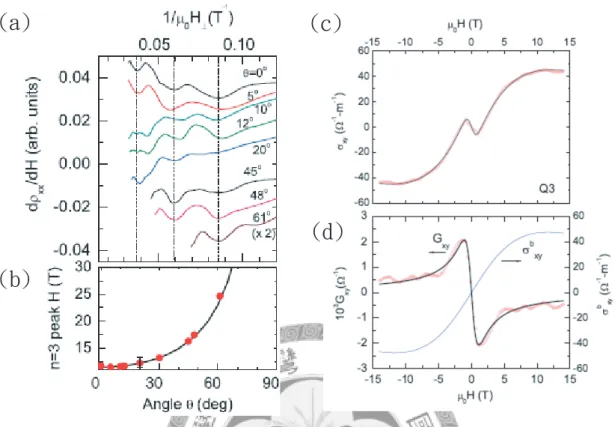
[22, 23, 24] that has a larger band-gap and a single Dirac cone. However, despite the high mobility (∼104 cm2/Vs) and low carrier concentration (∼1017cm−3) achieved, SdH os- cillations are still dominated by 3D bulk band in the pristine Bi2Se3. Although Ca doping can shift Fermi level into bulk band-gap [13, 25], SdH oscillations turn out to disappear also [26]. Only in SbxBi2−xSe3 with carrier concentration as low as 2.9×1016 cm−3and magnetic field up to 60T, SdH oscillations originating from 2D surface states was finally observed [27]. This technique was latter used on pristine, non-metallic Bi2Te3 crystals with very low carrier concentration (∼1015cm−3) [4]. In Fig. 1.6a, the resistivity deriva- tive dρxx/dH of a non-metallic Bi2Te3 was plotted against the inverse perpendicular field 1/H⊥at different angles. Where H⊥ ≡ H cos θ is the magnetic field component perpen-
)b*
)c*
)d*
)e*
Figure 1.6: Identification of surface states in non-metallic Bi2Te3, data from Ref. [4].
(a)The resistivity derivative dρxx/dH versus inverse perpendicular field. Where H⊥ ≡ H cos θ, is the magnetic field component perpendicular to the sample cleavage plane. The minima fall on the same vertical lines, indicating a 2D Fermi surface. (b)Field position of the resistivity minimum (which corresponds to the ν = 3 Landau level) plots against field angle (red dots), which follows the 1/ cos θ trend (black solid curve) up to 30T. (c)Hall conductivity versus magnetic field (red circles), and its best fit to Eq. 1.6 in solid black line. The non-linearity at low field cannot be explained by one band model. (d)Surface term (red circles) and bulk term (solid thin line) of Hall conductivity extracted from (c).
dicular to the sample cleavage plane. We can see that the minima fall on the same vertical lines, indicating a 2D Fermi surface. In Fig. 1.6b, field position of a particular resistivity minimum (which corresponds to ν=3) was plotted against the field angle θ in red dots, which follows the 1/ cos θ trend (black solid curve) up to 30T as expected for a 2D Fermi surface (Fig. 4.3). The recent studies of the angular dependence of fSdH in the topological insulator Bi2Te2Se also showed similar results [28, 29], making this method probably the most promising way of identifying the surface states by transport measurements.
Another evidence of a 2D surface state in non-metallic Bi2Te3comes from an anomaly of Hall conductivity observed at low field. From semiclassical expression, the Hall con-
ductivity σxy of electrons in a single band, closed orbit under uniform magnetic field is
σxy = neµ µB
[1 + (µB)2], (1.5)
where n is carrier concentration, e is electron charge, and µ is the mobility. At small field, σxycan be approximated by neµ2B. That is, if there are more than one parallel conducting bands each described by Eq. 1.5, the total Hall conductivity will be dominated by the band with large µ. This was first observed in non-metallic Bi2Te3crystals [4]. Figure 1.6c plots the Hall conductivity against magnetic field (red circles). A clear non-linearity can be seen at low field, which cannot be explained by the single band models, such as Eq. 1.5. Now, consider a two band model composed of one 3D band and one 2D band. The total Hall conductivity
σtotalxy = σbxy+ Gxy/t, (1.6)
where t is the sample’s thickness, σxyb and Gxy are Hall conductivity from the bulk band and sheet Hall conductance from the surface states, respectively. Both σbxyand Gxy can be described by Eq. 1.5 (note that for Gxy, n in Eq. 1.5 is the sheet carrier concentration). The fitted curve is plotted in Fig. 1.6c in solid black line, which fits the data points very well.
Surface term (red circles) and bulk term (solid thin line) of Hall conductivity extracted from (c) are plotted in Fig. 1.6d. The obtained surface carrier density and mobility are in good agreement with the results extracted from SdH oscillations, suggesting that the observed anomaly truly comes from the 2D surface states. Similar results were also found in recent studies on the topological insulator Bi2Te2Se [28, 30]. Since the mobility in the surface states is typically larger than bulk bands due to backscattering suppression, Hall conductivity at low field can provide another way to identify the surface states.
1.3 Superconductivity in Misfit Compounds
Misfit compounds (also known as incommensurate compounds) are alternating stacking of two layer compounds (Fig. 1.7a) defined by the formula: (MX)1+x(TX2)n, with M=Sn,
Pb, Bi, Sb, rare earth elements; T=V, Ti, Cr, Nb, Ta; X=S, Se, Te; 0.08≤x≤0.28; n=1, 2, 3. The MX and TX2 sets possess its own symmetry and lattice constants. The misfit behaviour arises from the non-stoichiometry of the lattice constants between the adjacent layers in a certain direction. Let the misfit lattice constant be a1 and a2for MX and TX2, respectively. Lattice constant b and c are the same for the two sets, where c is chosen as the stacking direction (Fig. 1.7a). Misfit compound can be viewed as the host compound TX2 intercalated by MX, which is a two-atom layer with distorted NaCl structure (Fig. 1.7b).
The TX2set is a three-atom layer with structure depending on the atom T. The non-integer number 1 + x in the formula is determined by the ratio of the periodicities of the two sets (1 + x = 2(a2/a1)), and n is the number of TX2 sets sandwiched between the MX sets. The adjacent layers are held together simply by van-der-Waals force. Thus misfit compound is also a quasi-low-dimensional system.
Some of the host compounds (TX2) display charge density wave (CDW) transition.
CDW is a special phase of periodic modulation of the conduction electron density and the lattice atoms’ positions [31, 5, 32]. The modulation is usually a few percent in electron density and about one percent in lattice constant. Figure 1.8b shows the charge density, atom positions, and band structure of a normal conductor (the upper figure) and a CDW phase (the lower figure). The normal conductor has evenly distributed electron density and lattice atoms. The CDW shows periodic modulation of electron density and lattice atom distance. Such modulation opens up a narrow gap near Fermi surface and lowers the system’s total energy (right part of Fig. 1.8b). CDW is similar to superconductors in the way that they both opens up a gap near Fermi surface and have a collective conduction mode. When an electric field is applied, the CDW can “slide” relative to the lattice atoms.
The oscillating lattice atoms produces a travelling potential which results in a current (Fig. 1.8a). It is widely believed that CDW competes with superconductivity [33] and a lot of efforts have been made on reducing CDW transition temperature and increase superconductivity transition temperature [34, 35, 36]. However, some evidences showed
that CDW may coexist with superconductivity [37, 38, 34]. How do the same electrons participate in both transitions remains an open question. It is, therefore, a major task to search for new materials with coexisting CDW and superconductivity, which can provide a platform for studying the interplay between the two transitions. Misfit compound can be useful in studying this issue in the sense that superconductivity can occur within TX2, which originally displays CDW transition.
Another interesting topic in misfit compounds is the charge transfer between TX2 and MX sets. The MX and TX2 sets usually have carrier concentrations comparable to semiconductors separately, but the resulting misfit compound often displays carrier con- centration comparable to a metal. It is believed that electrons are transferred to TX2from MX layers [39]. The rigid band model was adopted to explain the charge transfer. It assumes that the electron D.O.S. of the misfit compound can be inferred from the super- position of its constituents’ D.O.S. [40]. Figure 1.7c is an example of how electrons are transferred from MX layers (PbSe) to the TX2layers (TiSe2). While the rigid band model can qualitatively explain the charge transfer in many misfit compounds, it fails to provide quantitative explanation [41]. Therefore, the detailed relation between charge transfer and the suppression of CDW or emergence of superconductivity is still unclear. Detailed experimental characterization of the electronic structure of misfit compounds will help to understand the issue.
c
a1
a2
b
b
(TX2)n
MX MX
c
a1
a2
b
b
(TX2)n
MX MX
)b* )c*
)d*
Figure 1.7: (a)Schematic drawing of the structure of a typical misfit compound. (b)The structure of a typical MX compound. (c)An example of how the rigid band model explains charge transfer in misfit compounds. This picture is from Ref. [42]
)b* )c*
Figure 1.8: (a)Schematic of how the collective behaviour of CDW results in a net current when electric field is applied. The solid lines and open circles indicate snapshots of the CDW and lattice atoms at successive times, respectively. (b)Schematic of how atom positions and electron density are modulated in CDW. The band structure is shown on the right. A narrow band gap opens up at±kF and the system’s total energy is lowered. The pictures are from Ref. [5].
Experimental Setup
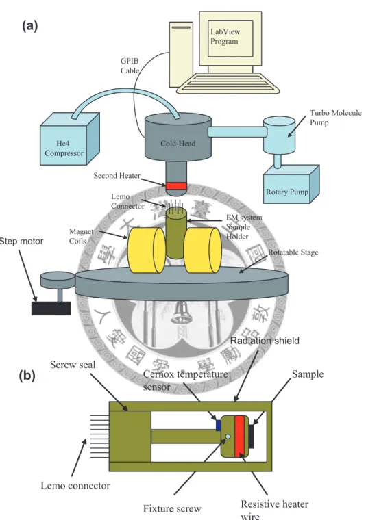
2.1 Superconducting Magnet System
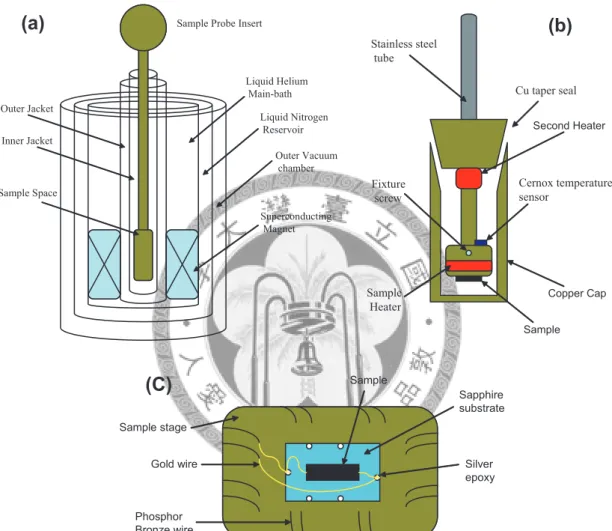
The superconducting magnet system (Oxford Instrument) is used for measurements that require high magnetic field. With a home-made two-jacket insert, sample temperature can be easily controlled from 4.2K to 300K with great stability better than 0.1%. A schematic drawing of the system is shown in Fig. 2.1a.
The superconducting coils are immersed in liquid helium (LHe) main bath at 4.2K.
The cryostat is shielded from the outside by a 77K liquid nitrogen reservoir and an outer vacuum shroud. The two-jacket insert is loaded from the top of the cryostat, and the sample probe is placed inside the inner jacket. The magnet is connected to a power sup- ply (IPS120, Oxford Instruments) that can be controlled by LabView program. At LHe temperature, the superconducting coils can sustain a supercurrent that produces a mag- netic field up to 15T. By using Lamda point fridge, LHe temperature around the coils can further drop to 2.2K, allowing the magnet to supply a field up to 17T.
The sample probe consists of a copper sample stage, which has 8 twisted pairs of phosphor bronze wires thermally anchored on it by Stycast Epoxy. A schematic drawing of sample stage is shown in Fig. 2.1(b) and (c). The stage is vacuum sealed by a taper copper can, and can be rotated and fixed at arbitrary angles from 0 to 90 degrees, allowing
16
different field orientation with respect to the sample. A 25Ω wire resistor is fixed on the sample stage to act as a sample heater. A Cernox temperature sensor (Lakeshore) is mounted on the back of sample stage to monitor the sample temperature. Both heater and sensor are connected to a temperature controller (Lakeshore 340). We can obtain proper cooling power through the LHe main bath by tuning the amount of helium exchange gas in the two jackets and the sample space. Precise temperature control is achieved by carefully tuning the PID parameters and the amount of helium exchange gas. The two jackets and sample space are kept under high vacuum with pressure∼ 10−6 torr using a pumping station before loading into the dewar. A liquid nitrogen (LN2) cold-trap is placed along the pump line to reduce possible oil vapour contamination.
2.2 Electromagnet System
The electromagnet system is designed for measurements that require different magnetic field orientation and also precise field control over the range±0.7T. The system consists of a 4K closed cycle refrigerator (Sumitomo) and a water cooled electromagnet (GMW), which can produce magnetic field up to 0.7T with pole gap size ∼41mm. A schematic drawing is shown in Fig. 2.2.
The electromagnet is placed on a rotatable stage where it’s angular position can be programmed. The magnetic field is controlled by a bipolar current supply (Kepco) and monitored by a Hall probe type gaussmeter (Lakeshore) with sensitivity∼0.1 Oe. The cold-head is connected to a helium compressor through a flexible high-pressure line. The cold-head temperature can go down to 3.8K if thermal insulation to outside is carefully treated. The sample space temperature can be well controlled by a local heater and tem- perature sensor, providing a feedback control on the setpoint. The sample holder and pumping station designs are similar to the superconducting magnet system described in the previous section.
Cu taper seal
Cernox temperature sensor
Fixture screw Stainless steel tube
Sample Heater
Copper Cap Second Heater
(b)
Sample
(C)
Sample stage
Gold wire
Phosphor Bronze wire
Sample
Sapphire substrate
Silver epoxy Liquid Helium
Main-bath Liquid Nitrogen Reservoir
Superconducting Magnet Sample Probe Insert
Outer Jacket
Inner Jacket
Sample Space
Outer Vacuum chamber
(a)
Figure 2.1: (a)Schematic of superconducting magnet system. (b)Side view of probe sam- ple space. Oxygen-free copper is used for sample stage to ensure good thermal conduc- tivity. The sample space is vacuum sealed by a taper copper can. The sample stage can be rotated and fixed at arbitrary angle from 0 to 90 degrees. (c)Schematic of how sample is mounted on the probe. Silver epoxy is used to anchor gold wires on sapphire, and silver paint is used to anchor gold wires on sample and phosphor bronze wires.
Rotary Pump Cold-Head
LabView Program
He4 Compressor
Turbo Molecule Pump
Lemo Connector
EM system Sample Holder GPIB
Cable
Magnet Coils
Rotatable Stage Second Heater
Screw seal
Cernox temperature sensor
Fixture screw Lemo connector
Resistive heater wire
Sample Radiation shield
(a)
(b)
Step motor
Figure 2.2: (a)Schematic of electromagnet system. The electromagnet is placed on a rotatable stage where it’s angular position can be programmed. (b)Side view of the sample holder. The holder is made of oxygen-free copper to ensure good thermal conductivity.
The sample is placed on a sample stage similar to the one in Fig. 2.1c.
2.3 Thin Film Deposition System
The thin film deposition system is composed of a magnetron sputtering chamber and an e-gun evaporation chamber. The two chambers are connected by a load-lock chamber, which can reach 5× 10⁻⁸ torr within 2 hours. It is equipped with a vertically movable stage such that samples can be easily reloaded from e-gun transfer rod to sputter transfer rod, or vice versa.
The e-gun chamber contains a 5-pocket electron source (Thermionics). Deposition rate and film thickness is monitored by a crystal oscillator (Maxtek). The chamber pres- sure is maintained at 5× 10⁻⁹ torr using an ion-pump (Varian) which is monitored by a hot-cathode ion gauge. Between the sample and crucible is a water cooled shield with a small round aperture in the middle to enhance collimation as well as prevent radiation heating on the sample.
The sputtering chamber contains three independent parts: the sample stage, shutter, and ion guns. The sample stage and shutter can rotate independently. There are four ion guns: three of them are sputtering sources and the fourth one is an Ar ion-milling source. A gas purifier (Centorr) is installed in order to minimize the oxygen content in the source gas. The chamber pressure is maintained at 5 × 10⁻⁹ torr by a cryopump (ULVAC CRYOGENICS) where the conductance is controlled by an Automatic Pressure Control Unit (MKS Instruments). The optimal pressure for thin film sputtering and Ar ion-milling are 6 mtorr and 0.1 mtorr, respectively. All the pressure gauges, gas valves, ion guns, sample stage and shutter are connected to a computer. Therefore, the whole sputtering process can be controlled by a programmed sequence.
2.4 Sample Preparation
2.4.1 Bulk Single crystals
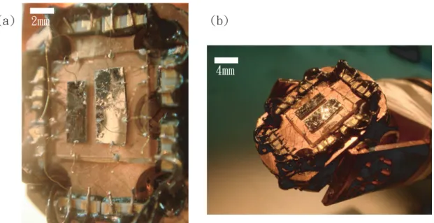
All the single crystal samples are provided by our collaborator (Dr. F.C. Chou’s laboratory at National Taiwan University). Bulk single crystals are first shaped into appropriate size and shape. Conventional 4-probe measurement is used for measuring resistivity and Hall effect (see Fig. 2.3a). The resistance R = VI = ρwℓ·t, where V is the voltage drop between voltage leads, I is the applied current, ρ is resistivity, ℓ is the distance between voltage leads, w is the width of sample, and t is the sample’s thickness. In order to maximize the measured signal V and also for the convenience of sample mounting, sample size is typically about 1∼5 mm in length, 1∼3 mm in width, and the thickness is usually the thinner the better. The samples are first cut into a slab with appropriate length and width by diamond saw, and then milled to desired thickness by sand paper. Some soft samples can be easily cleaved and shaped by razor blade into appropriate dimensions. The shaped sample is thermally anchored onto sapphire substrate using thermally conductive grease (Apiezon-N), and the sapphire substrate is again thermally anchored onto sample stage by the same grease. Sapphire is chosen because of it’s excellent thermal conductivity and electrical insulation. Fine gold wires (1 or 2 mil) are thermal anchored on sapphire substrate using silver epoxy (Epotek H20E). One end of the gold wires are attached to sample and the other to the probe using silver paint (SPI Supplies) as shown in Fig. 2.3.
If care is taken in all steps, contact size smaller than 300µm, contact resistance lower than 50Ω can be achieved.
For electrical transport measurements the resistivity tensor ρij can be determined through
Ei = ρijJj, (2.1)
where Ei is the measured electric field, and Jj the input current density. Note that we define z-axis as out-of-plane direction, and xy plane as in-plane, with i, j = (x, y). By
)b* 3nn )c*
5nn
Figure 2.3: (a)A photo showing two bulk single crystals connected to superconducting magnet sample probe by wire binding techniques described in the main context. The two black thin flakes in the center of picture with shining surfaces are single crystals to be measured. The transparent square substrate beneath them is sapphire, it was chosen for it’s excellent thermal conductivity and electrical insulation. The 16 leads surrounding the sapphire are probe leads made of phosphor bronze, and they are connected to the crystals through gold wires. (b)A photo of the front part of sample probe. The sample stage can be fixed at arbitrary angle with respect to field direction, as shown in the photo.
convention, x is defined as the current direction. For isotropic systems, ρxx = ρyy and ρxy = −ρyx. In this thesis, the in-plane resistivity parallel to current is denoted by ρxx
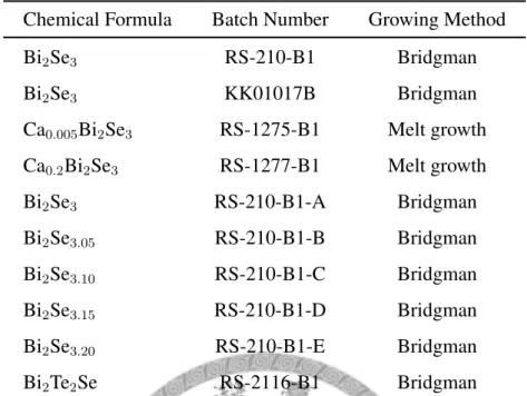
and the Hall resistivity (resistivity in-plane and transverse to current) is denoted by ρyx. The main difficulty in identifying the surface states of Bi2Se3is that the Fermi surface often lies inside bulk conduction band. We have tried to grow single crystals by melt growth, Bridgman method and vapour transport (CVT) (table 2.1 and table 3.1) under different temperature gradients. However, Fermi surface in those samples are still in the bulk conduction band. We have tried several other attempts on tuning the Fermi surface into the bulk band-gap. One of the attempts is through doping. It has been reported that calcium doping can tune the Fermi surface into bulk band-gap without degrading the surface states [13]. The resistivity of the doped single crystals show non-metallic temperature dependence and the value at 4K is two orders of magnitude larger than the undoped Bi2Se3 [26]. Another attempt is to increase the ratio of selenium in the Bi2Se3
Topological Insulator Sample List
Chemical Formula Batch Number Growing Method
Bi2Se3 RS-210-B1 Bridgman
Bi2Se3 KK01017B Bridgman
Ca0.005Bi2Se3 RS-1275-B1 Melt growth
Ca0.2Bi2Se3 RS-1277-B1 Melt growth
Bi2Se3 RS-210-B1-A Bridgman
Bi2Se3.05 RS-210-B1-B Bridgman
Bi2Se3.10 RS-210-B1-C Bridgman
Bi2Se3.15 RS-210-B1-D Bridgman
Bi2Se3.20 RS-210-B1-E Bridgman
Bi2Te2Se RS-2116-B1 Bridgman
Table 2.1: A list of the batch numbers and growing methods of the topological insulator crystals presented in this thesis.
crystals. It was suggested in some papers that the n-type doping in as-grown Bi2Se3 is mainly caused by selenium vacancies [43] and the carrier concentration can be varied by adding excess amount of selenium [44, 23]. Table 2.1 is a list of the batch numbers and growing methods of the topological insulator crystals presented in this thesis. Our goal is to prepare a crystal that has high mobility and in-gap Fermi level, which allows us to identify the surface states through quantum oscillations. Recently, it was reported that Bi2Te2Se is a chemically more stable topological insulator [45]. This compound is formed by substituting the selenium at the quintuple layer boundary (Se1 and Se1’ in Fig.1.3c) in Bi2Se3with tellurium atoms. Selenium atoms tend to escape Bi2Se3crystals, leaving behind vacancies at the boundary of quintuple layers. This problem is much less severe if the boundary atoms are tellurium, which is also less sensitive to air compared with selenium. Therefore, Bi2Te2Se is chemically more stable than Bi2Se3. Fermi surface of the as-grown Bi2Te2Se is in the bulk band-gap, and the RT curve shows non-metallic behavior [29, 28]. We have recently succeeded in growing such non-metallic crystals.
The transport data of all the crystals listed in table 2.1 will be given in section 3.1.
Misfit Compound Sample List
Chemical Formula Batch Number Growing Method
(SnS)(TaS2) RS-1115-B1 CVT
(SnS)(TaS2)2 RS-1120-B1 CVT
(PbSe)(TiSe2)2 RS-1142-B1 CVT
Table 2.2: A list of the batch numbers and growing methods of the misfit compounds presented in this thesis.
2.4.2 Micro-sized Devices
The micro-sized crystals are transferred onto p-type Si substrate with 300nm thermal oxide using conventional mechanical exfoliation technique [46]. We used a model similar to the one described in several papers for graphene to determine the thickness of exfoliated crystals under optical microscope (OM) [47, 48](Fig. 2.4). According to our simulation, thermal oxide layer of 300nm gives the best contrast under the illumination of green light (λ=550nm). On the other hand, the simulations on graphene suggest that the result of this wavelength is closest to the experimental results in our lab. The refractive index of SiO2
and Si in our simulation are 1.546 and 4.09− 0.044i, respectively, (from Ref. [49]). The refractive index of Bi2Se3 is 4.996 + 2.8× 10⁻⁵i, which is calculated using the dielectric constant (ε = 24.96 + 2.78× 10⁻⁴i) found in Ref. [50]. The contrast is defined by
C ≡ I(SiO2)− I(Bi2Se3)
I(SiO2) , (2.2)
where I(SiO2) and I(Bi2Se3) are the intensity of light reflected from SiO2 and Bi2Se3, respectively. Unfortunately, our simulation result doesn’t agree with the experimental ob- servation. It suggests an oscillating contrast with respect to crystal thickness (Fig. 2.5a).
However, the contrast obtained from experiment (Fig. 2.5b) appears to vary unsystemati- cally for different thickness ranging from 10∼100 nm. One of the reasons is the relatively small size of our exfoliated crystals which makes contrast determination difficult. We also suspect that the contrast of crystal may saturate above 10 layers [48] (about 10nm in thickness), which is also the lower limit of the crystal thickness we can find for Bi2Se3.
SiO2 Bi2Se3 Air ( n=1 )
Si SiO2 Bi2Se3 Air ( n=1 )
Si
300nm d1
i n
n
i n
SiO I
Se Bi I SiO C I
Si SiO
Se Bi
044 . 0 09 . 4
546 . 1
10 8 . 2 996 . 4
) (
) (
) (
2 3 2
5 2
3 2 2
−
=
=
× +
=
≡ −
− Incident Light ӳ= 550 nm
Figure 2.4: Schematic of the model and parameters used for Bi2Se3 OM contrast sim- ulation. The light path is perpendicular to sample plane. The refractive index for each material are labeled. The contrast is defined as the intensity of light reflected by SiO2 wafer, minus the intensity of light reflected by crystal, then divided by the intensity of SiO2 wafer reflection. The Thickness of SiO2 is 300nm. Bi2Se3thickness is the indepen- dent variable denoted by d1.
)b* )c*
Figure 2.5: (a)Simulation data of Bi2Se3 OM contrast with respect to sample thickness on 300nm SiO2 wafer under green light illumination. The refractive index of Bi2Se3 is 4.996. (b)Experimental data points of Bi2Se3 OM contrast with respect to sample thick- ness on 300nm SiO2 wafer under white light illumination. The OM contrast is varying unsystematically with respect to sample thickness.
![Figure 1.3: The crystal structure of Bi 2 Se 3 (from Ref. [1]) (a)Crystal structure with three primitive lattice vectors denoted as t 1 , t 2 , and t 3](https://thumb-ap.123doks.com/thumbv2/9libinfo/9605125.631223/19.892.220.660.134.569/figure-crystal-structure-crystal-structure-primitive-lattice-vectors.webp)