Chapter 4
Design and Analysis of Integrated 32×32 Photonic Bandgap Wavelength Switch Based on SOI Waveguide
As mentioned in Chapter 3, the integrated development of optical waveguide devices has become the future trend. We propose optical waveguide components for DWDM device and Optical Switch building on SOI wafers by MMI technology in this chapter. This chapter is organized as follows: Section 4-1 introduces the technique of optoelectronic integrated circuits, SOI waveguide, and switch device. The advantages of SOI MMI waveguide applied in integrated optics are presented and discussed. The mathematical formulations of MMI structure are also briefly derived and discussed in Section 4-2. The characteristics of our designed 32×32 PBG wavelength switch components based on plasma effect by computer-aided BeamPROP_CAD software and introduction of a novel SOI Schottky electro-optical modulator [156] are presented in Section 4-3. We also give the conclusions and discussions of our designed 32×32 PBG wavelength switch devices in the final Section 4-4.
4-1 Introduction of Multi-Mode Interference Structure and Optical Wavelength Switch Device
In the recent years, many people paid attention to multimode interference (MMI) structure on integrated optical circuits. MMI devices
employing self-image in multimode waveguides have recently developed into key components for photonic integrated circuits and optical communication. Their unique properties, such as compact size [157], low loss [158-159], stable splitting ratio, low crosstalk and large optical bandwidth, insensitivity to polarization, ease of production, and good fabrication tolerances have led to their rapid incorporation in more complex photonic integrated circuits. According to the said, we can design and fabricate N×N couplers and 1×N splitters [160-166]. Various types of switches have been fabricated in varied semiconductor materials, including 3 dB couplers [167-169], 90 degree hybrids [170] and symmetric power splitters [171-172], Mach-Zehnder switches [173], optical coherent front-end polarization-diversity detector chip [174] and power splitters and combiners for ring laser [175-176].
Optical switches play a key role in routing and the other function in advanced optical networks, both for wavelength-division-multiplexed (WDM) and single-wavelength applications [177-178]. Many optical switches based on SOI, SiGe, and LiNbO3 had been published in some literatures [179-180]. Due to the CMOS electronic device can reach gigabits-per-second logic optical switch array can achieve on SOI wafer.
The optical phase modulators are designed in SOI optical switch very recently [181-185].
Recently, various switches based on multimode interference effects have been reported in literatures [186-188]. MMI couplers device have several advantage of eliminating optical confinement to change the waveguide behavior [189] and using a localized refractive index change to
alter the imaging length of the MMI coupler [190]. The modes supported in the MMI device can be selectively perturbed to change the optical field in the output port. Thus, the utility of the MMI device can be used as active switches. MMI switch operates by the selective perturbation of the modal index and the selective perturbation of the modal index is changed by the localized modification of the refractive index.
The change in the propagation constant of the MMI mode as follow:
The first order is proportional to the overlap integral of the optical intensity distribution with the altered refractive index region. If the latter lies symmetrically along the longitudinal axis of the MMI, then the overlap integrals for even-order modes will be larger than those for odd modes, with the result that is changed. In the first demonstration of such switching, J. C. Campbell and T. Li applied a voltage to a pair of closely spaced electrodes placed on either side of the central axis of a LiNbO3 multimode waveguide [191]. According to the above literature, we can add switching voltages to change the localized refractive index. The resulting localized refractive index change caused the light output to switch from one side of the device to the other.
4-2 Mathematical Formulation of Multi-Mode Interference
Recently, many people paid attention to multi-mode interference (MMI) structure on integrated optics circuits [192-193] because of small size, low loss, independent polarization, and high tolerance of fabrication parameters. In this section, we would derive some principles of multi-mode
v
interference. The relation of the lateral wavenumber and the propagation constant
kyv
β are related to the ridge refractive index can be derived dispersion equation as following equation [70]
nr
2 2 0 2 2
r v
yv k n
k +β = (4-2-1) with
0 0
2 λ
= π
k (4-2-2)
ev
yv W
k (v+1)π
=
where is the mode numbers, v λ0 is the free-space wavelength and is the effective width and corresponding to the fundamental mode as [193]
Wev
(
2 2)
122
0 −
⎟⎟ −
⎠
⎜⎜ ⎞
⎝
⎟⎛
⎠
⎜ ⎞
⎝ +⎛
=
≅ r c
r c M
e
ev n n
n W n
W W
σ
π
λ (4-2-3)
where is the ridge effective refractive index, is the cladding effective refractive index and is the width of the step-index multimode waveguide as shown in Fig. 4-1,
nr nc
WM
=0
σ for TE and σ =1 for TM. By using binomial expansion kyv2 <<k02nr2, the propagation constant
βv can be deduced from Eq. (4-2-1) to Eq. (4-2-3)
2 0 2
0 4
) 1 (
e r r
v nW
n v
k πλ
β = − + (4-2-4) Then we define as the beat length of the two lowest order mode ( =0,1).
Lπ
v
0 1
0 3
4 λ β
β π
π r e
W
L ≅ n
= − (4-2-5) The propagation constants spacing can be written as
( )
π
β π
β L
v v
v 3
) 2 (
0
≅ +
− (4-2-6)
4-3 Design and Analysis of Integrated 32 × 32 Photonic Bandgap Wavelength Switch Based on SOI Waveguide
Through the briefly introduction of multi-mode interference (MMI) and optical wavelength switch device, we apply them to design and simulate the characteristics of 32×32 channels optical wavelength switch waveguide for tuning the various wavelengths to various output ports. It is important to design and analyze the geometric parameters of waveguide structure for promoting the performance of optical device. In this section, we try to simulate the light propagating along the 32×32 PBG wavelength switch with the computer-aided BeamPROP_CAD software on MMI and SOI structure. The characteristics of guide-wave are propagating in 32×32 PBG wavelength switch waveguide devices with adding various voltages and electro-optical corresponding to our designed 32×32 PBG wavelength switch waveguide device based on MMI and SOI structure. They are also discussed in the following subsections.
4-3-1 Design and Analysis of 32 × 32 Photonic Bandgap Wavelength Switch with A Novel SOI Schottky Electro-Optical Modulator Based on MMI and SOI Substrate
In this section, we design an 32 × 32 photonic bandgap (PBG) electro-optical switch based on plasma effect. A novel SOI schottky electro-optical modulator was proposed by Marco Mazza et al. [156]. They demonstrate the performances of the SOI Schottky modulator has much better injection efficiency and significantly lower thermal effects than other conventional electro-optical modulators that use SOI p-i-n diodes. Via appropriate scaling down, the novel SOI Schottky modulator can achieve unrivaled GHz high speed switching. Fig. 4-1(a) shows the cross section of vertical Schottky diode in the SOI rib waveguide of a electro-optical modulator and Fig. 4-1(b) depicts the surface biopolar of the traditional pin diode solution for optical modulator. In the new SOI Schottky diode structure provides a full vertical injection of carriers and conduction. Fig.
4-2(a) shows the compare of the Schottky and traditional p-i-n diode structure in current density characteristics. The Schottky diodes present a lower threshold voltage than traditional p-i-n diode. Fig. 4-2(b) shows the refractive index modulation in a SOI Schottky and traditional p-i-n modulator. It is demonstrated that the Schottky modulator shows a significantly increased refractive index modulation because of better injection efficiency and a reduced self-heating. Hence, we consider using
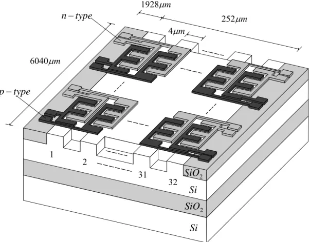
the novel SOI Schottky electro-optical modulator to design our 32×32 PBG wavelength switch. The 32×32 PBG wavelength switch with adding various voltages on several fingered electrode pad regions. The refractive index changes in the modulator mechanism also are calculated with adding various voltages on several fingered electrode pad regions. Fig. 4-3 shows the schematic diagram of the 32×32 PBG wavelength switch waveguide. It is composed of three regions such as 32 channels single mode SOI rib waveguide at both input and output plane, MMI structure and fingered electrode pads. The major portion of our device is designed the fingered electrode pads based on MMI structure. The total length and total width of the 32×32 PBG wavelength switch is 6040µm and 252µm, respectively. In the 32 channels single mode SOI rib waveguide at both input and output plane, the size we designed of the single mode SOI rib waveguide width and length at both input and output ports are 4µm and 100µm, respectively.
The height of the top silicon layer (device layer) is 5µm, and the slab height is 3.67µm can be implemented by using UNIBOND SOI wafer. The buried oxide layer is 1µm and the cladding layer is composed of air and oxide layer. In the MMI structure, the length and width of the MMI structure is 6040µm and 252µm, respectively. In the fingered electrode pads, it is composed of two regions such as the positive electrodes (anode) and the negative electrodes (cathode). Fig. 4-4 shows the top view of our designed fingered electrode pads based on MMI structure. The dot regions are the p-type and n-type regions and the dark regions are electrode pads.
The electrode pads are above doping regions and are composed of 256 cells
fingered electrode pads. The radius r of doping regions at p-type and n-type regions are 0.4µm and the lattice constant is 1µm. The distances of each fingered electrode pad at the horizontal and vertical are 1µm and 340µm, respectively. The width and length of the both anode and cathode in a cell of fingered electrode pad are 5µm and 340µm, respectively. The distance between the anode and cathode is 1µm and the overlap length of a cell fingered electrode pad is 3µm. The number of anode and cathode in a cell fingered electrode pad are 85 pairs and the period number of anode and cathode are identical 4µm.
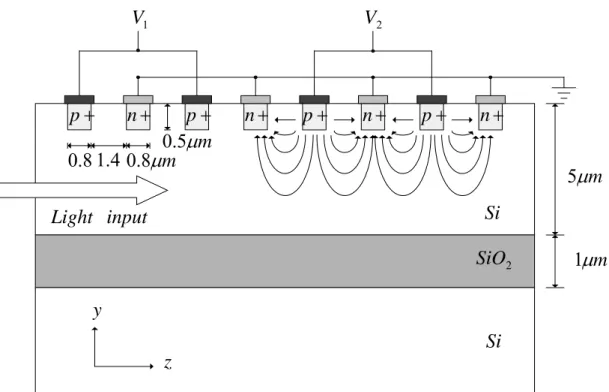
a
Fig. 4-5 shows a longitudinal cut view of the optical SOI PBG wavelength switch. The depth of the doping electron-hole pair concentration is 0.5µm. The width of doping regions at p-type and n-type regions are identical 0.8µm and the distance between p-type and n-type regions is 1.4µm. The distance between doped regions has been kept short enough and has been made quasi-periodic in order to produce possible formation of Bragg refractors. In the MMI structure, we implant p-type boron and n-type phosphorus on the upper layer of the SOI waveguide to form p-i-n structure. The major structures are the diodes, doped region and the contacts. These structures are lying on the same plane and fully compatible with CMOS technology. Diodes pairs connected in parallel and instead of a single lateral diode all along the waveguide structure. In the new SOI Schottky diode structure provides a full vertical injection of carriers and conduction. Due to the structures, we allow also much more uniform injection of charge. We could obtain electron and holes concentration changes in the modulator mechanism and calculate the
refractive index changes in the modulator mechanism via adding various voltages. There are several doping regions that are composed by p-type and n-type in MMI structure. The injected carrier concentration (holes) in p-type region is about Np=2×1017 cm-3. The carrier concentration (electrons) is exceeding Nn=1018 cm-3. Via the Drude model, we can get the various change of refractive index (∆n) from –1.0×10⁻³ to –1.6×10⁻² with several electro-optical modulator [7,156]. Therefore we add voltage on the top contact above p-type regions, the average change of refractive index that is induced by the plasma effect will reduce the refractive index of intrinsic silicon. According to the above condition, we can add various voltages on fingered electrode pad to get various change of refractive index.
4-3-2 Design and Analysis of Integrated 32 × 32 Photonic Bandgap Wavelength Switch with the Refractive Index Change –1.6×10⁻²
In this section, we design an 32 × 32 PBG wavelength switch waveguide based on plasma effect by BeamPROP_CAD. We simulate the phase shift effect and the optical wavelength switch with adding various voltages on several fingered electrode pad regions. The refractive index changes in the modulator mechanism also are calculated with adding various voltages on several fingered electrode pad regions. Fig. 4-6 shows the top view of our designed 32×32 SOI PBG wavelength switch with 256
0324 0424 0524 0608 0708 0808
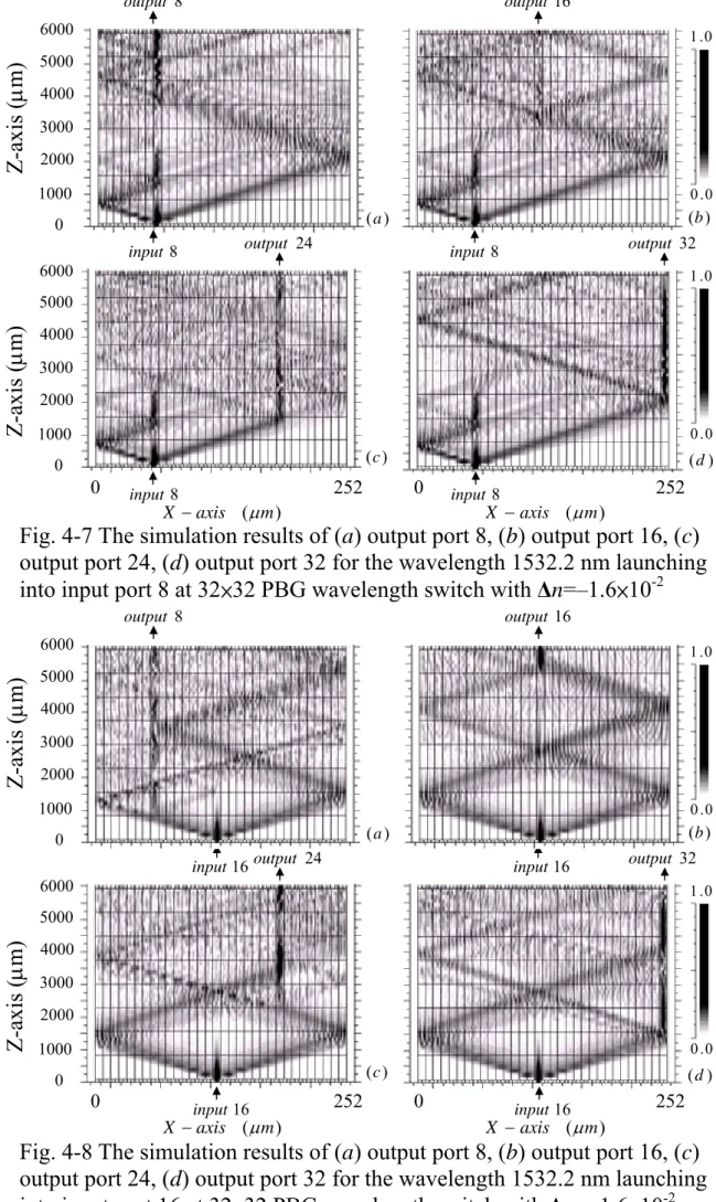
cells fingered electrical pads. The number of fingered electrode pad at the horizontal and vertical are 32 and 8, respectively. With tuning the voltages on several fingered electrode pads and use the different change of refractive index on several regions to control the light wave propagation path. In addition to all of the above, we can switch the light wave propagate from one of 32 input channels to one of 32 output channels at will. Fig. 4-7 shows a light wavelength 1532.2nm launching into input port8 at our designed 32 × 32 PBG wavelength switch. Fig. 4-7(a) shows a light wavelength 1532.2nm propagate from input8 to output8 and the transmittance value of the output8 is –9.51dBm. We add voltages on several fingered electrode pads such as , , , , ,
, , and use the change of refractive index ( =–1.6×10 M0108 M0208 M0308 M0408 M0508
M0608 M0708 M0808 ∆n -2) on several regions to control the light wave propagation path. Fig. 4-7(b) shows a light wavelength 1532.2nm propagate from input8 to output16 and the transmittance value of the output16 is –8.97 dBm. We add voltages on several fingered electrode pads such as , , , , , , , and use the change of refractive index ( =–1.6×
10
M0116 M0216 M0316 M0416 M0516
M0608 M0708 M0808 ∆n
-2)on several regions to control the light wave propagation path. Fig.
4-7(c) shows a light wavelength 1532.2nm propagate from input8 to output24 and the transmittance value of the output24 is –13.39 dBm. We add voltages on several fingered electrode pads such as , ,
, , , , , and use the change of refractive M0124 M0224
M M M M M M
index ( ∆n=–1.6 × 10⁻²) on several regions to control the light wave propagation path. Fig. 4-7(d) shows a light wavelength 1532.2nm propagate from input8 to output32 and the transmittance value of the output32 is –12.85 dBm. We add voltages on several fingered electrode
pads such as , , , , , , , ,
and use the change of refractive index (
M0132 M0232 M0332 M0432 M0532 M0608 M0708 M0808
M0430 ∆n=–1.6×10⁻²) on several
regions to control the light wave propagation path.
Fig. 4-8 shows a light wavelength 1532.2nm launching into input port16 at our designed 32×32 PBG wavelength switch. Fig. 4-8(a) shows a light wavelength 1532.2nm propagate from input16 to output8 and the transmittance value of the output8 is –15.01 dBm. We add voltages on several fingered electrode pads such as , , , , ,
, , , , and use the change of refractive index ( =–1.6×10
M0108 M0208 M0308 M0408 M0508
M0608 M0708 M0616 M0716 M0816
∆n -2) on several regions to control the light wave propagation path. Fig. 4-8(b) shows a light wavelength 1532.2nm propagate from input16 to output16 and the transmittance value of the output16 is –8.55 dBm. We add voltages on several fingered electrode pads such as ,
, , , , , , and use the change of
refractive index (
M0116
M0216 M0316 M0416 M0516 M0616 M0716 M0816
∆n=–1.6×10⁻²) on several regions to control the light wave propagation path. Fig. 4-8(c) shows a light wavelength 1532.2nm propagate from input16 to output24 and the transmittance value of the output24 is –8.71 dBm. We add voltages on several fingered electrode pads
such as , , , , , , , and use the change of refractive index (
M0124 M0224 M0324 M0424 M0524 M0616 M0716 M0816
∆n=–1.6×10⁻²) on several regions to control the light wave propagation path. Fig. 4-8(d) shows a light wavelength 1532.2nm propagate from input16 to output32 and the transmittance value of the output32 is –12.70 dBm. We add voltages on several fingered
electrode pads such as , , , , , , ,
, and use the change of refractive index (
M0132 M0232 M0332 M0432 M0532 M0632 M0732
M0716 M0816 ∆n=–1.6×10⁻²) on
several regions to control the light wave propagation path.
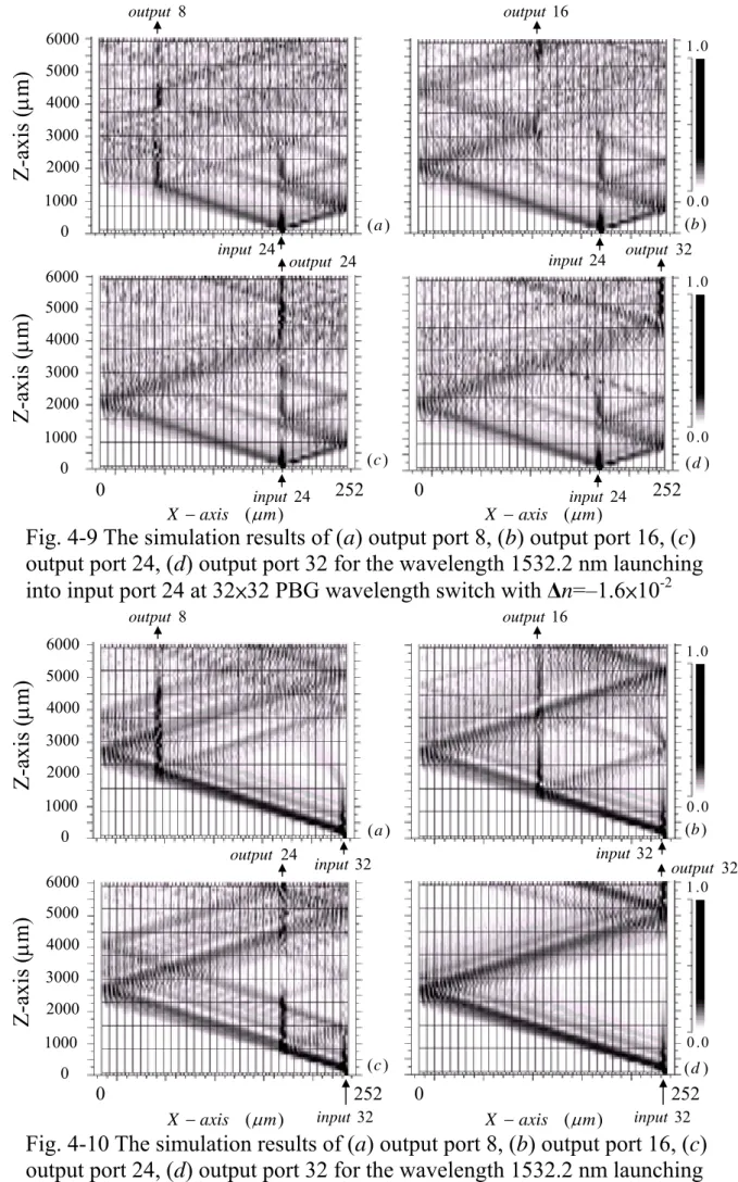
Fig. 4-9 shows a light wavelength 1532.2nm launching into input port24 at our designed 32×32 PBG wavelength switch. Fig. 4-9(a) shows a light wavelength 1532.2nm propagate from input24 to output8 and the transmittance value of the output8 is –15.89 dBm. We add voltages on several fingered electrode pads such as , , , , ,
, , , , and use the change of refractive index ( =–1.6×10
M0108 M0208 M0308 M0408 M0508
M0608 M0708 M0624 M0724 M0824
∆n -2) on several regions to control the light wave propagation path. Fig. 4-9(b) shows a light wavelength 1532.2nm propagate from input24 to output16 and the transmittance value of the output16 is –12.63 dBm. We add voltages on several fingered electrode pads such as ,
, , , , , , , and use the
change of refractive index ( =–1.6×10
M0116
M0216 M0316 M0416 M0516 M0616 M0624 M0724 M0824
∆n -2) on several regions to control the light wave propagation path. Fig. 4-9(c) shows a light wavelength
1532.2nm propagate from input24 to output24 and the transmittance value of the output24 is –13.82 dBm. We add voltages several fingered electrode
pads such as , , , , , , , and
use the change of refractive index (
M0124 M0224 M0324 M0424 M0524 M0624 M0724 M0824
∆n=–1.6×10⁻²) on several regions to control the light wave propagation path. Fig. 4-9(d) shows a light wavelength 1532.2nm propagate from input24 to output32 and the transmittance value of the output32 is –9.92 dBm. We add voltages on several fingered electrode pads such as , , , , ,
, , and use the change of refractive index ( =–1.6×10 M0132 M0232 M0332 M0432 M0532
M0624 M0724 M0824 ∆n -2) on several regions to control the light wave propagation path.
Fig. 4-10 shows a light wavelength 1532.2nm launching into input port32 at our designed 32×32 PBG wavelength switch. Fig. 4-10(a) shows a light wavelength 1532.2nm propagate from input32 to output8 and the transmittance value of the output8 is –18.05 dBm. We add voltages on several fingered electrode pads such as , , , , ,
, , and use the change of refractive index ( =–1.6×10 M0108 M0208 M0308 M0408 M0508
M0608 M0732 M0832 ∆n -2) on several regions to control the light wave propagation path. Fig. 4-10(b) shows a light wavelength 1532.2nm propagate from input32 to output16 and the transmittance value of the output16 is –12.16 dBm. We add voltages on several fingered electrode pads such as , , ,
, , , , , , , and use the
change of refractive index ( =–1.6×10
M0116 M0216 M0316
M0416 M0516 M0616 M0716 M0532 M0632 M0732 M0832
∆n -2) on several regions to control the
light wave propagation path. Fig. 4-10(c) shows a light wavelength 1532.2nm propagate from input32 to output24 and the transmittance value of the output24 is –7.15 dBm. We add voltages on several fingered
electrode pads such as , , , , , , ,
, , , and use the change of refractive index ( =–1.6×10
M0124 M0224 M0324 M0424 M0524 M0624 M0724
M0824 M0632 M0732 M0832
∆n -2) on several regions to control the light wave propagation path. Fig. 4-10(d) shows a light wavelength 1532.2nm propagate from input32 to output32 and the transmittance value of the output32 is –6.35 dBm. We add voltages on several fingered electrode pads such as ,
, , , , , , and use the change of
refractive index (
M0132
M0232 M0332 M0432 M0532 M0632 M0732 M0832
∆n=–1.6×10⁻²) on several regions to control the light wave propagation path.
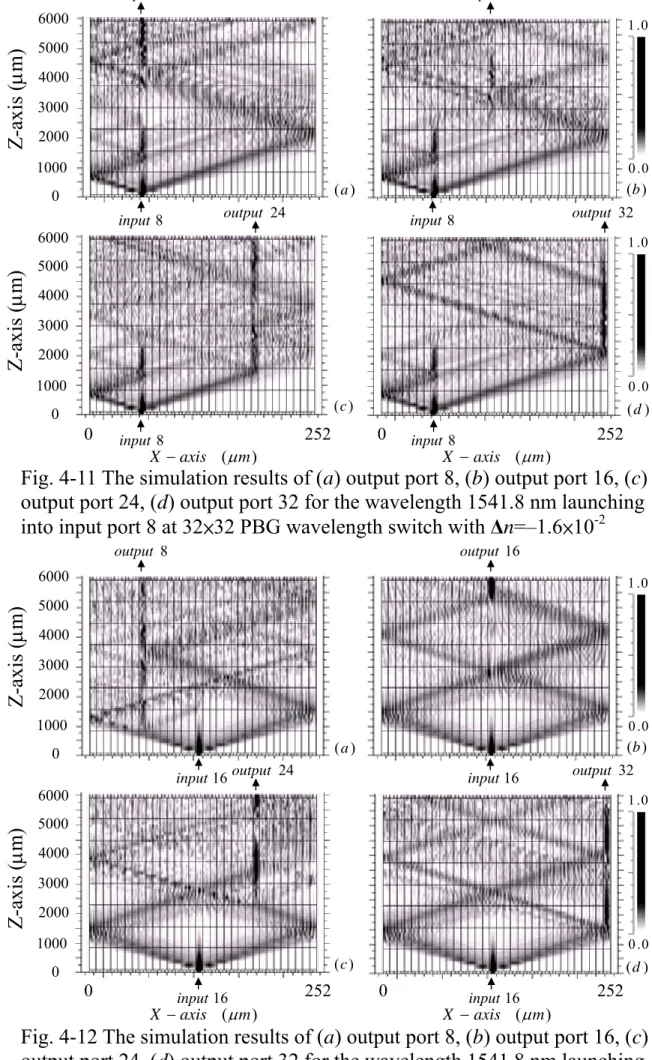
Fig. 4-11 shows a light wavelength 1541.8nm launching into input port8 at our designed 32×32 PBG wavelength switch. Fig. 4-11(a) shows a light wavelength 1541.8nm propagate from input8 to output8 and the transmittance value of the output8 is –7.81 dBm. We add voltages on several fingered electrode pads such as , , , , ,
, , and use the change of refractive index ( =–1.6×
10
M0108 M0208 M0308 M0408 M0508
M0608 M0708 M0808 ∆n
-2)on several regions to control the light wave propagation path. Fig.
4-11(b) shows a light wavelength 1541.8nm propagate from input8 to output16 and the transmittance value of the output16 is –14.43 dBm. We add voltages on several fingered electrode pads such as M0116, M0216,
M0316, , , , , and use the change of refractive index ( =–1.6 × 10
M0416 M0516 M0608 M0708 M0808
∆n -2) on several regions to control the light wave propagation path. Fig. 4-11(c) shows a light wavelength 1541.8nm propagate from input8 to output24 and the transmittance value of the output24 is –17.46 dBm. We add voltages on several fingered electrode
pads such as , , , , , , , and
use the change of refractive index (
M0124 M0224 M0324 M0424 M0524 M0608 M0708 M0808
∆n=–1.6×10⁻²) on several regions to control the light wave propagation path. Fig. 4-11(d) shows a light wavelength 1541.8nm propagate from input8 to output32 and the transmittance value of the output32 is –20.17 dBm. We add voltages on several fingered electrode pads such as , , , , ,
, , and use the change of refractive index ( =–1.6×10 M0132 M0232 M0332 M0432 M0532
M0608 M0708 M0808 ∆n -2) on several regions to control the light wave propagation path.
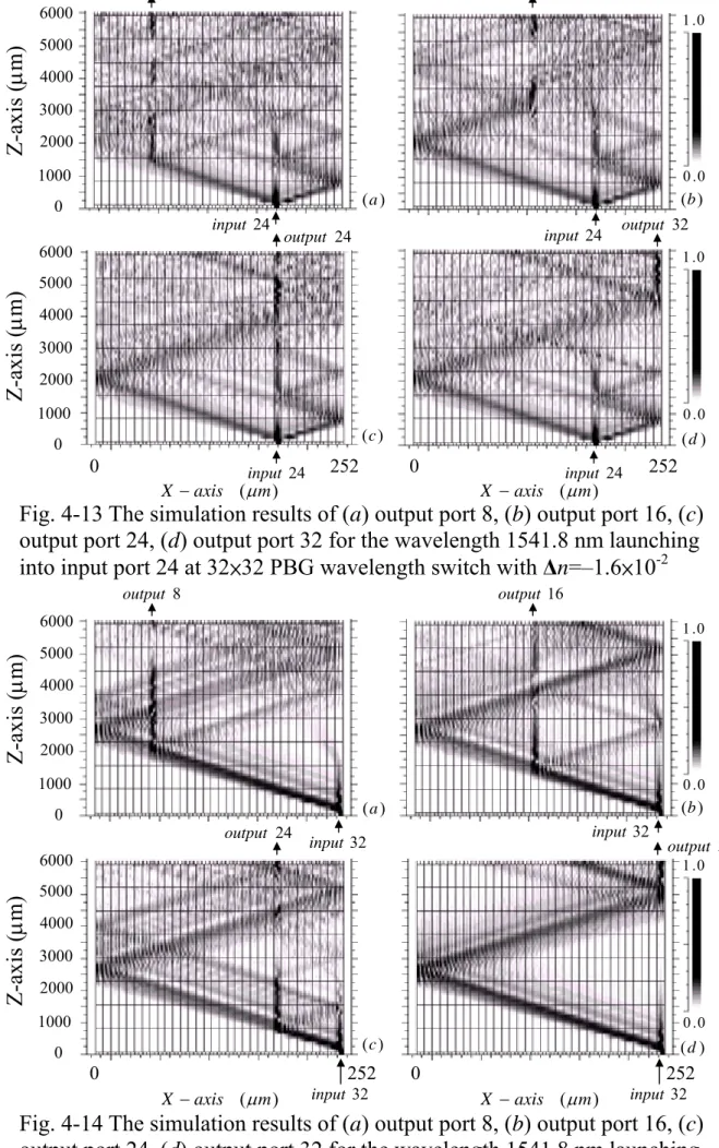
Fig. 4-12 shows a light wavelength 1541.8nm launching into input port16 at our designed 32×32 PBG wavelength switch. Fig. 4-12(a) shows a light wavelength 1541.8nm propagate from input16 to output8 and the transmittance value of the output8 is –15.57 dBm. We add voltages on several fingered electrode pads such as , , , , ,
, , , , and use the change of refractive index ( =–1.6×10
M0108 M0208 M0308 M0408 M0508
M0608 M0708 M0616 M0716 M0816
∆n -2) on several regions to control the light wave propagation path. Fig. 4-12(b) shows a light wavelength 1541.8nm propagate from input16 to output16 and the transmittance value of the output16 is –5.31
dBm. We add voltages on several fingered electrode pads such as ,
, , , , , , and use the change of
refractive index (
M0116
M0216 M0316 M0416 M0516 M0616 M0716 M0816
∆n=–1.6×10⁻²) on several regions to control the light wave propagation path. Fig. 4-12(c) shows a light wavelength 1541.8nm propagate from input16 to output24 and the transmittance value of the output24 is –9.29 dBm. We add voltages on several fingered electrode pads
such as , , , , , , , and use
the change of refractive index (
M0124 M0224 M0324 M0424 M0524 M0616 M0716 M0816
∆n=–1.6×10⁻²) on several regions to control the light wave propagation path. Fig. 4-12(d) shows a light wavelength 1541.8nm propagate from input16 to output32 and the transmittance value of the output32 is –15.98 dBm. We add voltages on several fingered
electrode pads such as , , , , , , ,
, and use the change of refractive index (
M0132 M0232 M0332 M0432 M0532 M0632 M0732
M0716 M0816 ∆n=–1.6×10⁻²) on
several regions to control the light wave propagation path.
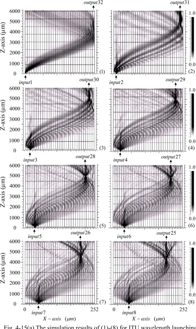
Fig. 4-13 shows a light wavelength 1541.8nm launching into input port24 at our designed 32×32 PBG wavelength switch. Fig. 4-13(a) shows a light wavelength 1541.8nm propagate from input24 to output8 and the transmittance value of the output8 is –12.46 dBm. We add voltages on several fingered electrode pads such as , , , , ,
, , , , and use the change of refractive index ( =–1.6×10
M0108 M0208 M0308 M0408 M0508
M0608 M0708 M0624 M0724 M0824
∆n -2) on several regions to control the light wave propagation
path. Fig. 4-13(b) shows a light wavelength 1541.8nm propagate from input24 to output16 and the transmittance value of the output16 is –13.45 dBm. We add voltages on several fingered electrode pads such as ,
, , , , , , , and use the
change of refractive index ( =–1.6×10
M0116
M0216 M0316 M0416 M0516 M0616 M0624 M0724 M0824
∆n -2) on several regions to control the light wave propagation path. Fig. 4-13(c) shows a light wavelength 1541.8nm propagate from input24 to output24 and the transmittance value of the output24 is –11.44 dBm. We add voltages on several fingered
electrode pads such as , , , , , , ,
and use the change of refractive index (
M0124 M0224 M0324 M0424 M0524 M0624 M0724
M0824 ∆n=–1.6×10⁻²) on several
regions to control the light wave propagation path. Fig. 4-13(d) shows a light wavelength 1541.8nm propagate from input24 to output32 and the transmittance value of the output32 is –14.53 dBm. We add voltages on several fingered electrode pads such as , , , , ,
, , and use the change of refractive index ( =–1.6×10 M0132 M0232 M0332 M0432 M0532
M0624 M0724 M0824 ∆n -2) on several regions to control the light wave propagation path.
Fig. 4-14 shows a light wavelength 1541.8nm launching into input port32 at our designed 32×32 PBG wavelength switch. Fig. 4-14(a) shows a light wavelength 1541.8nm propagate from input32 to output8 and the transmittance value of the output8 is –20.71 dBm. We add voltages on several fingered electrode pads such as , , , , ,
, , and use the change of refractive index ( =–1.6×10 M0108 M0208 M0308 M0408 M0508
0608 0732 0832
M M M ∆n -2)
on several regions to control the light wave propagation path. Fig. 4-14(b) shows a light wavelength 1541.8nm propagate from input32 to output16 and the transmittance value of the output16 is –14.90 dBm. We add voltages on several fingered electrode pads such as , , ,
, , , , , , , and use the
change of refractive index ( =–1.6×10
M0116 M0216 M0316
M0416 M0516 M0616 M0716 M0532 M0632 M0732 M0832
∆n -2) on several regions to control the light wave propagation path. Fig. 4-14(c) shows a light wavelength 1541.8nm propagate from input32 to output24 and the transmittance value of the output24 is –12.01 dBm. We add voltages on several fingered
electrode pads such as , , , , , , ,
, , , and use the change of refractive index ( =–1.6×10
M0124 M0224 M0324 M0424 M0524 M0624 M0724
M0824 M0632 M0732 M0832
∆n -2) on several regions to control the light wave propagation path. Fig. 4-14(d) shows a light wavelength 1541.8nm propagate from input32 to output32 and the transmittance value of the output32 is –10.17 dBm. We add voltages on several fingered electrode pads such as ,
, , , , , , and use the change of
refractive index (
M0132
M0232 M0332 M0432 M0532 M0632 M0732 M0832
∆n=–1.6×10⁻²) on several regions to control the light wave propagation path.
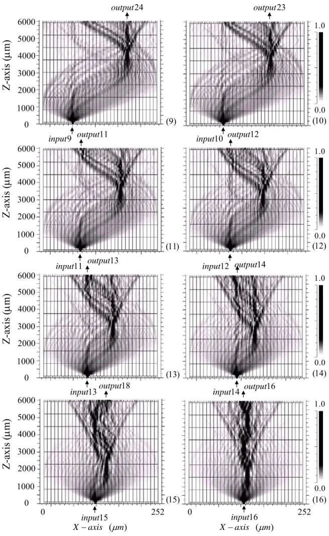
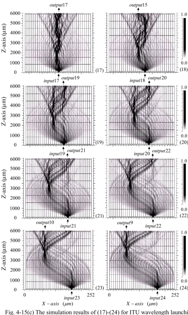
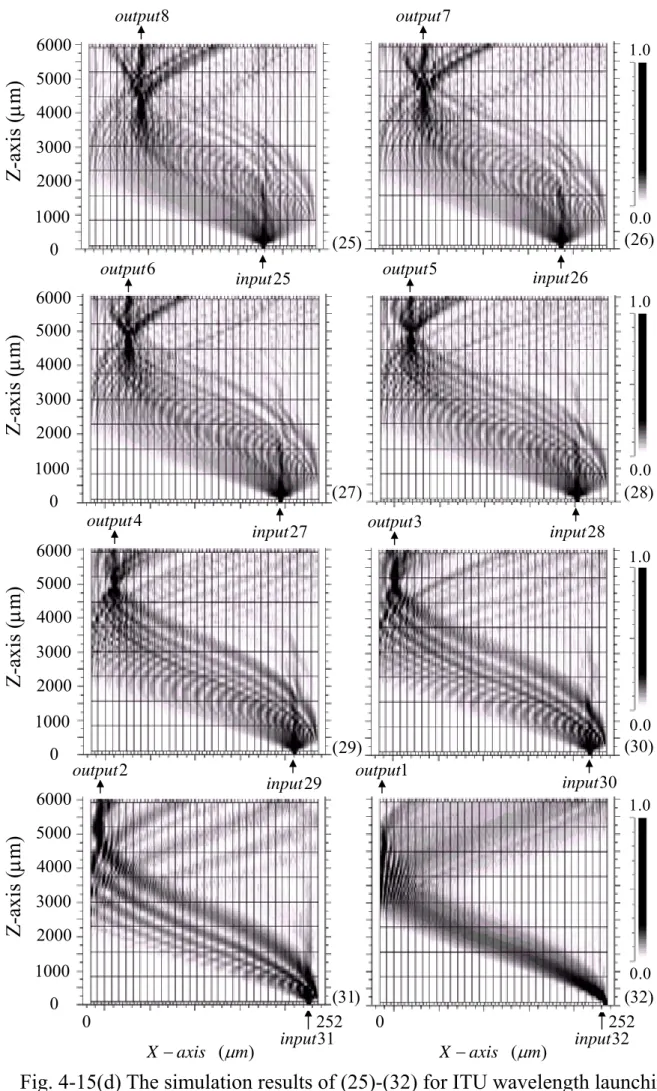
Fig. 4-15 shows an ITU light wavelength from 1532.2 nm to 1541.8nm launching into each input port from channel1 to channel32 at our designed 32×32 PBG wavelength switch individually. The total number of our input wavelength is 32 and the channel spacing is 0.4nm. In this case,
16
i i17
we add voltages on several fingered electrode pads and use the various change of refractive index from –1.0×10⁻³ to –1.6×10⁻² on several regions to control the light wave propagation path. The regions of adding voltages and the change of refractive index on several fingered electrode pads such as
= =–1.6 × 10
01
Mi Mi32 -2, Mi02 = Mi31 =–1.5 × 10⁻², Mi03 = Mi30 =–1.4 × 10⁻²,
= =–1.3 × 10
04
Mi Mi29 -2, Mi05 = Mi28 =–1.2 × 10⁻², Mi06 = Mi27 =–1.1 × 10⁻²,
= =–1.0 × 10
07
Mi Mi26 -2, Mi08 = Mi25 =–9.0 × 10⁻³, Mi09 = Mi24 =–8.0 × 10⁻³,
= =–7.0 × 10
10
Mi Mi23 -3, Mi11 = Mi22 =–6.0 × 10⁻³, Mi12 = Mi21 =–5.0 × 10⁻³,
= =–4.0 × 10
13
Mi Mi20 -3, Mi14 = Mi19 =–3.0 × 10⁻³, Mi15 = Mi18 =–2.0 × 10⁻³,
= =–1.0×10
M M -3 and where the is positive integral number ( =01, 02, …, 08).
i i
Fig. 4-15(a) shows the simulation results of (1)-(8) for ITU wavelength from 1532.2nm to 1535nm launching into 32 × 32 PBG wavelength switch from input port1 to input port8. Fig. 4-15(a)-(1) show a light wavelength 1532.2nm propagate from input1 to output32 and the transmittance value of the output32 is –23.57 dBm. Fig. 4-15(a)-(2) show a light wavelength 1532.6nm propagate from input2 to output31 and the transmittance value of the output31 is –10.57 dBm. Fig. 4-15(a)-(3) show a light wavelength 1533nm propagate from input3 to output30 and the transmittance value of the output30 is –14.69 dBm. Fig. 4-15(a)-(4) show a light wavelength 1533.4nm propagate from input4 to output29 and the transmittance value of the output29 is –10.39 dBm. Fig. 4-15(a)-(5) show a
light wavelength 1533.8nm propagate from input5 to output28 and the transmittance value of the output28 is –7.10 dBm. Fig. 4-15(a)-(6) show a light wavelength 1534.2nm propagate from input6 to output27 and the transmittance value of the output27 is –9.86 dBm. Fig. 4-15(a)-(7) show a light wavelength 1534.6nm propagate from input7 to output26 and the transmittance value of the output26 is –12.37 dBm. Fig. 4-15(a)-(8) show a light wavelength 1535nm propagate from input8 to output25 and the transmittance value of the output25 is –10.06 dBm.
Fig. 4-13(b) shows the simulation results of (9)-(16) for ITU wavelength from 1535.4nm to 1538.2nm launching into 32 × 32 PBG wavelength switch from input port9 to input port16. Fig. 4-15(b)-(9) show a light wavelength 1535.4nm propagate from input9 to output24 and the transmittance value of the output24 is –17.79 dBm. Fig. 4-15(b)-(10) show a light wavelength 1535.8nm propagate from input10 to output23 and the transmittance value of the output23 is –20.59 dBm. Fig. 4-15(b)-(11) show a light wavelength 1536.2nm propagate from input11 to output11 and the transmittance value of the output11 is –8.96 dBm. Fig. 4-15(b)-(12) show a light wavelength 1536.6nm propagate from input12 to output12 and the transmittance value of the output12 is –15.07 dBm. Fig. 4-15(b)-(13) show a light wavelength 1537nm propagate from input13 to output13 and the transmittance value of the output13 is –9.78 dBm. Fig. 4-15(b)-(14) show a light wavelength 1537.4nm propagate from input14 to output14 and the transmittance value of the output14 is –17.45 dBm. Fig. 4-15(b)-(15) show a light wavelength 1537.8nm propagate from input15 to output18 and the transmittance value of the output18 is –14.68 dBm. Fig. 4-15(b)-(16) show
a light wavelength 1538.2nm propagate from input16 to output16 and the transmittance value of the output16 is –6.45 dBm.
Fig. 4-15(c) shows the simulation results of (17)-(24) for ITU wavelength from 1538.6nm to 1541.4nm launching into 32 × 32 PBG wavelength switch from input port17 to input port24. Fig. 4-15(c)-(17) show a light wavelength 1538.6nm propagate from input17 to output17 and the transmittance value of the output17 is –12.66 dBm. Fig. 4-15(c)-(18) show a light wavelength 1539nm propagate from input18 to output15 and the transmittance value of the output15 is –8.23 dBm. Fig. 4-15(c)-(19) show a light wavelength 1539.4nm propagate from input19 to output19 and the transmittance value of the output19 is –9.33 dBm. Fig. 4-15(c)-(20) show a light wavelength 1539.8nm propagate from input20 to output20 and the transmittance value of the output20 is –9.46 dBm. Fig. 4-15(c)-(21) show a light wavelength 1540.2nm propagate from input21 to output21 and the transmittance value of the output21 is –16.72 dBm. Fig. 4-15(c)-(22) show a light wavelength 1540.6nm propagate from input22 to output22 and the transmittance value of the output22 is –9.53 dBm. Fig. 4-15(c)-(23) show a light wavelength 1541nm propagate from input23 to output10 and the transmittance value of the output10 is –24.37 dBm. Fig. 4-15(c)-(24) show a light wavelength 1541.4nm propagate from input24 to output9 and the transmittance value of the output9 is –16.71 dBm.
Fig. 4-15(d) shows the simulation results of (25)-(32) for ITU wavelength from 1541.8nm to 1544.6nm launching into 32 × 32 PBG wavelength switch from input port25 to input port32. Fig. 4-15(d)-(25)
show a light wavelength 1541.8nm propagate from input25 to output8 and the transmittance value of the output8 is –10.45 dBm. Fig. 4-15(d)-(26) show a light wavelength 1542.2nm propagate from input26 to output7 and the transmittance value of the output7 is –14.04 dBm. Fig. 4-15(d)-(27) show a light wavelength 1542.6nm propagate from input27 to output6 and the transmittance value of the output6 is –11.28 dBm. Fig. 4-15(d)-(28) show a light wavelength 1543nm propagate from input28 to output5 and the transmittance value of the output5 is –6.69 dBm. Fig. 4-15(d)-(29) show a light wavelength 1543.4nm propagate from input29 to output4 and the transmittance value of the output4 is –11.31 dBm. Fig. 4-15(d)-(30) show a light wavelength 1543.8nm propagate from input30 to output3 and the transmittance value of the output3 is –14.47 dBm. Fig. 4-15(d)-(31) show a light wavelength 1544.2nm propagate from input31 to output2 and the transmittance value of the output2 is –9.82 dBm. Fig. 4-15(d)-(32) show a light wavelength 1544.6nm propagate from input32 to output1 and the transmittance value of the output1 is –23.39 dBm.
4-3-3 Design and Analysis of Integrated 32 × 32 Photonic Bandgap Wavelength Switch with the Refractive Index Change –4.0×10⁻³
In this section, we design an 32 × 32 PBG wavelength switch waveguide based on plasma effect. We simulate the phase shift effect and the optical wavelength switch with adding various voltages to change the
0708 0808
refractive index change on several fingered electrode pad regions. The max value of the refractive index change is –4.0×10⁻³. Fig. 4-16 shows a light wavelength 1532.2nm launching into input port8 at our designed 32×32 PBG wavelength switch. Fig. 4-16(a) shows a light wavelength 1532.2nm propagate from input8 to output8 and the transmittance value of the output8 is –13.12 dBm. We add voltages on several fingered electrode pads such as
, , , , , , , and use the
change of refractive index ( =–4.0×10
M0108 M0208 M0308 M0408 M0508 M0608 M0708 M0808
∆n -3) on several regions to control the light wave propagation path. Fig. 4-16(b) shows a light wavelength 1532.2nm propagate from input8 to output16 and the transmittance value of the output16 is –10.31 dBm. We add voltages on several fingered electrode
pads such as , , , , , , , ,
, , , , , and use the change of refractive index ( =–4.0 × 10
M0116 M0216 M0316 M0416 M0516 M0616 M0716 M0816
M0608 M0708 M0808 M0111 M0211 M0311
∆n -3)on several regions to control the light wave propagation path. Fig. 4-16(c) shows a light wavelength 1532.2nm propagate from input8 to output24 and the transmittance value of the output24 is –13.48 dBm. We add voltages on several fingered electrode
pads such as , , , , , , , ,
, and use the change of refractive index (
M0124 M0224 M0324 M0424 M0524 M0624 M0724 M0824
M M ∆n=–4.0×10⁻³) on
several regions to control the light wave propagation path. Fig. 4-16(d) shows a light wavelength 1532.2nm propagate from input8 to output32 and the transmittance value of the output32 is –13.8 dBm. We add voltages on