Large-scale “atomistic” approach
to discrete-dopant-induced characteristic
fluctuations in silicon nanowire transistors
Yiming Li*
, Chih-Hong Hwang**
, and Hsuan-Ming Huang***
Department of Communication Engineering, National Chiao Tung University, 1001 Ta-Hsueh Road, Hsinchu 300, Taiwan Received 8 October 2007, revised 30 January 2008, accepted 30 January 2008
Published online 15 May 2008
PACS 05.40.–a, 31.15.bt, 61.72.uf, 85.30.Tv
*** Corresponding author: e-mail [email protected], Phone: +886 3 5712121 ext. 52974, Fax: +886 3 5726639
*** e-mail [email protected], Phone: +886 3 5712121 ext. 52993, Fax: +886 3 5726639 *** e-mail [email protected], Phone: +886 3 5712121 ext. 59233, Fax: +886 3 5726639
© 2008 WILEY-VCH Verlag GmbH & Co. KGaA, Weinheim
1 Introduction Ion implantation, diffusion and ther-mal annealing induce significant random fluctuations in the physical and electrical characteristics of nanometer scale metal – oxide – semiconductor field effect transistors (MOS-FETs). Effects of different randomness on device charac-teristics have recently been studied both experimentally and theoretically [1 – 20]. Fluctuations of characteristics are caused not only by a variation in an average doping density, which is associated with a fluctuation in the number of im-purities, but also with a particular random distribution of impurities in the channel region. Moreover, fluctuations are particularly pronounced as the spatial scale of doping and oxide thickness variations become comparable with the dimensions of devices [3, 10, 11]. The International Technology Roadmap for Semiconductors has forecasted a transition from conventional bulk devices to silicon-on-insulator (SOI) devices, and then to multiple-gate SOIs as
high-performance devices [21]. Consequently, nanoscale devices with vertical channel structures, such as double-, triple- and surrounding-gate fin-typed FETs (FinFETs) are of great interest [22 – 24]. Among them, nanowire FinFETs are ultimate structures and potential candidates for next generation high-speed and high-power electronic devices. However, due to the manufacturability, nanowire transis-tors with a perfect gate structure (i.e., a surrounding gate with 100% gate-coverage ratio) theoretically are not al-ways guaranteed. Therefore, impact of non-ideal nanowire gate-coverage ratio on immunity against discrete-dopant-induced fluctuations is crucial in determining the behav-iour of nanoscale semiconductor devices and results in a compromise between the device performance and manu-facturability.
Diverse computational approaches, such as small-signal analysis [1 – 3], drift-diffusion (DD) [4 – 6] and Nanowire fin-typed field effect transistors (FinFETs) are
ul-timate structures and potential candidates for next generation nanoelectronic devices. Due to the limitation of manufactura-bility, nanowire transistors with a perfect gate structure (i.e., a surrounding gate with 100% gate-coverage ratio) theoretically are not always guaranteed. Impact of the discrete dopants on device performance is crucial in determining the behaviour of nanoscale semiconductor devices. The immunity of nanowire transistor against random discrete-dopant-induced fluctuation may suffer from the variation of gate-coverage-ratio. There-fore, in this paper, we for the fist time study the impact of non-ideal gate coverage on immunity against random-dopant-induced fluctuations for nanowire FinFETs. A 3D statistically
sound “atomistic” approach for analyzing random-dopant ef-fect in nanodevice is presented. Discrete dopants are statisti-cally positioned into the channel region to examine associated carrier transportation characteristics, concurrently capturing “dopant concentration variation” and “dopant position fluc-tuation”. Our results confirm that the influence of non-ideal gate coverage disturbs the channel controllability of nanowire FinFETs and thus decreases the immunity against discrete-dopant-induced fluctuation. This study provides an insight into the problem of fluctuation in nanowire transistors and shows the importance of gate-coverage ratio on device’s im-munity against discrete-dopant-induced fluctuation.
Monte Carlo simulation [7 – 9] have recently been reported to study fluctuation-related issues in semiconductor de-vices. Unfortunately, the effect of the number and position of discrete dopants on the characteristics of the aforemen-tioned devices has not been clearly investigated yet. This study thus tries to employ a statistically sound “atomistic” approach to analyze the random impurity effect in nano-scale device, concurrently capturing “dopant concentration variation” and “dopant position fluctuation”. The statisti-cally generated large-scale doping profiles are similar to the physical process of ion implantation and the number of impurities inside channel follows normal distribution. Based on the statistically generated large-scale doping pro-files, each device simulation is performed by solving a set of 3D DD equations with quantum corrections by the den-sity gradient method [25, 26]. Thus, the intrinsic physical variation and characteristic fluctuations can be examined properly. All statistically generated discrete dopants are incorporated into the large-scale 3D device simulation running on our parallel computing system [27 – 29]. It has been known that very similar DC characteristics of nanowire transistor could be maintained whenever the gate-coverage-ratio varies from 70% to 100% [23]. Never-theless, the immunity of nanowire transistor against ran-dom-dopant-induced characteristic fluctuation may signifi-cantly suffer from the variation of gate-coverage-ratio. Our results show that the influence of non-ideal gate-coverage ratio disturbs the channel controllability of nanowire tran-sistors and thus decreases the immunity against discrete-dopant-induced fluctuation. Increase of characteristic fluc-tuation reveals the importance of gate-coverage ratio on
Characteristic adjustment for nominal case
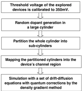
Random dopant generation in a large cylinder
Partition the whole cylinder into sub-cylinders
Mapping the partitioned cylinders into the device’s channel region
Simulation with a set of drift-diffusion equations with quantum corrections by the
density gradient method Threshold voltage of the explored
devices is calibrated to 350mV.
Figure 1 A simulation flow of the presented 3D statistically
sound “atomistic” approach to analyze random dopant effect in nanodevices. The physical parameters used in the 3D DD equa-tions are quantitatively verified with the experimental data of planar and nanowire devices [10, 11, 22, 30]. The large-scale computation is conducted in our cluster system [29].
nanowire device’s immunity against discrete-dopant-induced fluctuation.
The paper is organized as follows. In Section 2, a sta-tistically sound “atomistic” approach for analyzing the ran-dom impurity effect in nanoscale device is introduced. In Section 3, discrete-dopant-induced characteristic fluc-tuations of nanowire transistor with surrounding- and omega-gate structures are examined. Finally we draw con-clusions.
2 Simulation techniques The simulation flow is
shown in Fig. 1; to have the same device’s operation point, the threshold voltage of the explored devices is calibrated to 350 mV. The nominal channel doping concentration of the studied is 1.48 × 10⁻¹⁸ cm–3. They have a 16 nm gate, an 8 nm diameter and a gate oxide thickness of 1.2 nm. Out-side the channel, the doping concentrations in the source and drain are 3 × 1020 cm–3. This study considers the n-type silicon nanowire transistors, where boron dopants are used in the p-type channel. For the simplicity, only those dopants within the channel region are treated discretely. Inside the discrete dopant region, to include the effect of random fluctuation of the number and position of discrete dopants, we first generate a large number of dopants in a long cylinder solid, in which the equivalent doping concen-tration is equal to 1.48 × 10⁻¹⁸ cm–3. The long cylinder solid is then partitioned into sub-cylinders with 16 nm gate. Each partitioned sub-cylinders are mapped into device channel region for the 3D “atomistic” device simulation. Characteristics of each device with discrete dopants are calculated by solving a set of 3D DD equations with quan-tum corrections by the density gradient method [25, 26]. In “atomistic” device simulation, the resolution of individual charges within a conventional DD simulation using a fine mesh creates problems associated with singularities in the Coulomb potential. The density gradient approximation is used to handle discrete charges by properly introducing the related quantum mechanical effects [26].
Figure 2(a) shows 149 dopants randomly generated in a 2000 nm length cylinder, in which the equivalent doping concentration is 1.48 × 1018 cm–3. The whole cylinder is then partitioned into 125 cylinders, where each sub-cylinder is with 16 nm length. The number of dopants in the sub-cylinder may vary from zero to five, and the aver-age number is equal to one, as shown in Fig. 2(b) – (d), re-spectively. These 125 sub-cubes are then mapped into the channel region of the device with different gate-coverage-ratio for the discrete dopant simulation, as shown in Fig. 2(e) – (g). All statistically generated discrete dopants are incorporated into the large-scale 3D device simulation running on the parallel computing system [27 – 29]. Ac-cording to this analyzing scenario, only channel dopants are treated discretely. The doping concentrations remain continuous in the source/drain region because the volume of source/drain region is two-order magnitude greater than that of channel region. With this respect the present simu-lations give a qualitative result. Nevertheless, this approach
Mean = 1 Dopants in 16nm Nanowire -1 0 1 2 3 4 5 6 H ist ogr a m (num be r) 0 10 20 30 40 50 60 ----3s3s3s3s +3s+3s+3s+3s 0 5 o Dopants i 16nm Nanowire -1 6 H ist ogr a m (num be r) 0 10 20 30 40 50 60
{
----3s3s3s3s +3s+3s+3s+3s 0 5 Cuttin lo d-d’ direction Surrounding -gate (100% coverage) Omega-gate (80% coverage) (f) (e)Silicon Nanowire ChannelNanowire Channel
Insulator
Insulator
Drain Drain Source
Source DrainDrain
Metal Gate Metal Gate d d’ Omega-gate (70% coverage) (g) (d) 5 dopants in a 16nm cylinder 0 dopants in a 16nm cylinder 16nm 16nm (a) (b) (c) Gate Mean = 1 n Silicon
}
0 1 2 3 4 5Figure 2 (online colour at: www.pss-a.com) (a) Discrete dopants
randomly distributed in the 2000 nm length cylinder with the av-erage concentration of 1.48 × 1018 cm–3. There will be 149 dopants within the cylinder and the number of dopants may vary from 0 to 5 (the average number is 1) within its 125 sub-cylinders of 16 nm length (plots of (b), (c), and (d)). These sub-cylinders are then equivalently mapped into the channel region (plots of (e), (f), and (g)), for discrete dopant simulation. We notice that the explored device now has different gate-coverage-ratios, they are (e) the surrounding-gate (i.e., 100% coverage), (f) the omega-gate with 80% coverage-ratio, and (g) the omega-gate with 70% cov-erage-ratio.
allows us to focus on the study of characteristic fluctua-tions induced by the randomness of the number and position of dopants in the channel simultaneously. The statistically sound 3D “atomistic” device simulation technique is also computationally cost-effective. We notice that the mobility model used in the device simulation, according to Mathiessen’s rule [31, 32], is expressed as:
surf-aps surf-rs bulk
1 D D 1 ,
µ = µ + µ + µ (1)
parts: (i) The surface contribution due to acoustic phonon scattering 0 surf-aps 1/3 0 ( / ) , ( / )i K B C N N E E T T τ µ = + (2)
where Ni is the total concentration of ionized impurities, T0 = 300 K, E is the transverse electric field normal to the interface of semiconductor and insulator, B and C are pa-rameters which are based on physically derived quantities, N0 and τ are fitting parameters, T is lattice temperature, and K is the temperature dependence of the probability of sur-face phonon scattering. (ii) The contribution attributed to surface roughness scattering is
1 3 ref surf-rs ( /E E ) E , Ξ µ δ η -Ê ˆ =Á + ˜ Ë ¯ (3)
where Ξ = +A ( (α n p N+ ) refv )/((Ni+N1) ),v Eref = 1 V/cm is a reference electric field to ensure a unitless numerator in µsurf-rs, N =refv 1 cm–3 is a reference doping concentration to cancel the unit of the term raised to the power v in the denominator of Ξ ,δ is a constant depending on the de-tails of the technology, such as oxide growth conditions, N1 = 1 cm–3, A, α and η are fitting parameters. (iii) The bulk mobility is bulk L 0 , T T ξ µ µ -Ê ˆ = Á ˜ Ë ¯ (4)
where µL is the mobility due to bulk phonon scattering and ξ is a fitting parameter. The mobility model is quantified with measured data of different FETs in our earlier work [10 – 13, 22, 29, 30] for the best accuracy.
3 Results and discussion This section first discusses the fluctuations of potential and current density due to dis-crete dopants; and then the impact of non-ideal nanowire gate-coverage ratio on immunity against discrete-dopant-induced fluctuations is studied. The on-state (the device is with the drain voltage VD = 1 V and the gate voltage VG = 1 V) potential distribution of the discretely doped case, shown in Fig. 3(a), and (b), are investigated to eluci-date the effect of discrete dopant on the potential and cur-rent distributions of the device. The potential fluctuations, shown in Fig. 3(b), are associated with the corresponding dopants in Fig. 3(d).
Comparison between Fig. 3(e) and (f) reveals that the current conducting path is disturbed and impeded by the discrete dopants locating at the channel. Since the potential distribution near the dopant is relatively negative in the channel, the dopant acts as a centre of a whirlpool-like electric field to repel electrons. As electrons transport from the end of source to the drain side, some of them will en-counter a negative electric field that is induced by the dis-crete dopants. The lateral electric field between the source
0.69 0.91 1.13 Potential (V) 0.69 0.91 1.13 Potential (V) On-State Potential; VD=1V VG=1V Sourc e (S) Drain (D) S D Nominal case (Continuously doped) Discretely dopant fluctuated case Cutting plane Channel Source Drain (a) (b) (e) (f) Source Drain 1.46x10⁷ 3.5x10⁷ Current Density (A/cm2) 1.46x10⁷ 3.5x10⁷
Current Density (A/cm2)
(c) (d)
Figure 3 (online colour at: www.pss-a.com) Comparison of the
on-state potential (a), (b) and the current density distributions (e), (f) of (c) the nominal case and (d) discretely doped cases. The po-tential fluctuations are induced by corresponding dopants in (d).
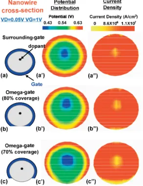
Figure 4 (online colour at: www.pss-a.com) Comparison of
po-tential (plots of (a′), (b′), and (c′)) and current density distribution (plots of (a″), (b″), and (c″)) in nanowire transistors with sur-rounding-gate (100% gate-coverage-ratio) and omega-gate (80% and 70% gate-coverage-ratio) structures.
Dopant Number 0 1 2 3 4 5 Vt h (V) 0.30 0.35 0.40 0.45 0.50 0.55 Surrounding-gate
Omega-gate with 80% gate coverage Omega-gate with 70% gate coverage
Figure 5 (online colour at: www.pss-a.com) Comparison of the
threshold voltage (Vth) fluctuation of the 16 nm gate silicon nanowire FET with surrounding-gate, omega-gate with 80%, and 70% gate-coverage-ratio.
and the drain, combined with the repulsion of the dopants, twists the electric field and increases the electron velocity near the dopants. The potential fluctuations not only alter the electric field and current conducting path, but also the electron velocity, and carrier mobility.
Figure 4 shows the comparisons of potential and cur-rent density distributions, respectively, for the nanowire transistors with the surrounding-gate (i.e., 100% gate-coverage-ratio) and the omega-gate (i.e., 80% and 70% gate-coverage-ratios) structures. The discrete dopants posi-tioned in the channel induce a potential fluctuation and substantially disturbs the current density distribution and the corresponding conduction path. The magnitude of po-tential and current density fluctuations is increased as the gate-coverage-ratio decreases. The non-ideal gate-coverage disturbs the channel controllability of the explored nano-wire transistors and thus decreases the immunity against discrete dopant induced fluctuation.
Ion (uA/um) 700 800 900 1000 1100 1200 Io ff (nA/um ) 0.0 0.1 0.2
0.3 Surrounding-gateOmega-gate with 80% gate coverage Omega-gate with 70% gate coverage
Figure 6 (online colour at: www.pss-a.com) Comparison of the
on – off state current (Ion – Ioff) fluctuation of the 16 nm gate sili-con nanowire FET with surrounding-gate, omega-gate with 80%, and 70% gate-coverage-ratio.
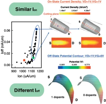
Off-State Potential Contour; VD=1V;VG=0V Ion (uA/um) 900 1000 1100 1200 Ioff (n A /u m ) 0.00 0.02 0.04 0.06 Similar Ioff S D S D S D S D 1 dopants Potential (V) 0.00V 0.39V 0.77V Potential (V) 0.00V 0.39V 0.77V D S D S 5 dopants S D S D S D S D S D S D
Figure 7 (online colour at: www.pss-a.com) Effect of
Discrete-Dopant-Position in silicon nanowire FET, where the devices are with different Ion but similar Ioff.
In our study, for a 16 nm gate silicon nanowire transis-tor, the threshold voltage fluctuations of the omega-gate devices with 80% and 70% gate-coverage are 1.04 and 1.19 times larger than that of the surrounding-gate struc-ture, as shown in Fig. 5. For current fluctuations, the ratio is 1.75 and 4.5 times larger than that of the surrounding-gate one, as shown in Fig. 6. The results confirm that the influence of non-ideal gate-coverage on the disturbances of
Ion (uA/um) 900 1000 1100 1200 Ioff (nA /u m ) 0.00 0.02 0.04 0.06 Ion (uA/um) 900 1000 1100 1200 Ioff (nA /u m ) 0.00 0.02 0.04 0.06
Off-State Potential Contour; VD=1V;VG=0V
Current Density (A/cm2)
1.46e7 2.92e7 4.38e7
Current Density (A/cm2)
1.46e7 2.92e7 4.38e7
On-State Current Density; VD=1V;VG=1V
Cutting plane 1 dopants Potential (V) 0.00V 0.39V 0.77V Potential (V) 0.00V 0.39V 0.77V D S D S S D S D S D S D S D S D S D S D S D Similar Ion Different Ioff D S 0 dopants
Figure 8 (online colour at: www.pss-a.com) Effect of
Discrete-Dopant-Position in silicon nanowire FET, where the devices are with similar Ion but different Ioff.
thus decreased.
Figure 7 shows the characteristics of the on-state and off-state currents (Ion – Ioff). For those cases with similar Ion, the maximum fluctuation of Ioff is within 0.05 nA/um. This figure discloses three different discrete-dopant channels, having similar values of Ion or Ioff but with various dopant positions. The cross-sectional on-state current density and off-state potential distributions extracting from the centre of channel are examined. Due to the difference of discrete dopant position, the different conduction paths of devices result in different on-state currents even we have very similar off-state currents, shown in Fig. 7. For the device having very similar on-state current with different off-state situations, Fig. 8 shows the off-state potential distribution at device’s channel. However, due to the effect of discrete dopant position, there is no potential barrier located in the channel region.
4 Conclusion In this study, a 3D statistically sound cost-effective “atomistic” approach for analyzing ran- dom dopant effect in nanowire devices has been present- ed. Discrete dopants are statistically positioned into the channel region to examine the associated carrier trans-portation characteristics, concurrently capturing “dopant concentration variation” and “dopant position fluctuation”. This study also investigated the impact of non-ideal nanowire gate-coverage ratio on immunity against dis-crete-dopant-induced fluctuations. The results have con-firmed that the influence of non-ideal gate-coverage dis-turbs the channel controllability of nanowire transis-tors and thus decreases the immunity against discrete dopant induced fluctuation. The increase of fluctuation shows that the importance of gate-coverage ratio on nanowire device’s immunity against discrete-dopant-induced fluctuation.
As dimension of device scales, the particular distribution of dopants in channel is not so obvious. Thus, we assumed a uniform distribution of dopants in this study. Moreover, we noted that the simulation results will be more accurate and give more physical insight if the positions of Si atoms are replaced with Boron dopants in device simulation. However, this may require huge computation time; for example, the adopted large-scale 3D simulation had cost about three months. The more physical assumption requires much more huge computation time. We are planning to conduct such an investigation in our future work.
Acknowledgements This work was supported by Taiwan
National Science Council (NSC) under Contract NSC-96-2221-E-009-210 and by the Taiwan Semiconductor Manufacturing Com-pany, Hsinchu, Taiwan under a 2006 – 2008 grant.
References
[1] Y. Li and S.-M. Yu, J. Comput. Electron. 5, 125–129 (2006).
[2] P. Andrei and I. D. Mayergoyz, J. Appl. Phys. 94, 7163– 7172 (2003).
[3] Y. Li and S.-M. Yu, Jpn. J. Appl. Phys. 45, 6860–6865 (2006).
[4] A. Asenov, IEEE Trans. Electron Devices 45, 2505–2513 (1998).
[5] D. J. Frank, Y. Taur, M. Ieong, and H.-S. P. Wong, VLSI Tech. Dig., 169 – 170 (1999).
[6] A. R. Brown, A. Asenov, and J. R. Watling, IEEE Trans. Nanotechnol. 1, 195–200 (2002).
[7] C. L. Alexander, G. Roy, and A. Asenov, IEEE Int. Electron Devices Meeting (IEDM 06), San Francisco, CA, 2006, DOI: 10.1109/IEDM.2006.346941.
[8] W. J. Gross, D. Vasileska, and D. K. Ferry, IEEE Electron Device Lett. 20, 463–465 (1999).
[9] C. J. Wordelman, and U. Ravaioli, IEEE Trans. Electron Devices 47, 410–416 (2000).
[10] F.-L. Yang, J.-R. Hwang, H.-M. Chen, J.-J. Shen, S.-M. Yu, Y. Li, and Denny D. Tang, Dig. Tech. Papers Symp. VLSI Tech., 208 – 209 (2007).
[11] F.-L. Yang, J.-R. Hwang, and Y. Li, Proc. IEEE Custom Integrated Circuits Conference (CICC), 691 – 694 (2006). [12] Y. Li, and C.-H. Hwang, Microelectron. Eng. 84, 2093–
2096 (2007).
[13] Y. Li, and C.-H. Hwang, J. Appl. Phys. 102, 084509 (2007). [14] Y. Li, and S.-M. Yu, IEEE Trans. Semicond. Manuf. 20,
432 – 438 (2007).
[15] H.-S. Wong, Y. Taur, and D. J. Frank, Microelectron. Reliab. 38, 1447–1456 (1999).
[16] R. W. Keyes, Appl. Phys. 8, 251–259 (1975).
[17] P. Francis, A. Terao, and D. Flandre, IEEE Trans. Electron Devices 41, 715–720 (1994).
[18] X.-H. Tang, V. K. De, and J. D. Meindl, IEEE Trans. VLSI Syst. 5, 369–376 (1997).
[19] P. A. Stolk, F. P. Widdershoven, and D. B. M. Klaassen, IEEE Trans. Electron Devices 45, 1960–1971 (1998).
[20] A. Asenov and S. Saini, IEEE Trans. Electron Devices 46, 1718 – 1724 (1999).
[21] http://www.itrs.net
[22] Y. Li, H.-M. Chou, and J.-W. Lee, IEEE Trans. Nanotech-nol. 4, 510–516 (2005).
[23] Y. Li and W. H. Chen, Proc. IEEE Conf. Nanotechnol. 2, 569 – 572 (2006).
[24] E. J. Nowak, I. Aller, T. Ludwig, K. Kim, R. V. Joshi, C.-T. Chuang, K. Bernstein, and R. Puri, IEEE Circuits Devices Mag. 20, 20–31 (2004).
[25] M. G. Ancona and H. F. Tiersten, Phys. Rev. B 35, 7959 – 7965 (1987).
[26] G. Roy, A. R. Brown, A. Asenov, and S. Roy, J. Comput. Electron. 2, 323–327 (2003).
[27] Y. Li and S.-M. Yu, J. Comput. Appl. Math. 175, 87–99 (2005).
[28] Y. Li, H.-M. Lu, T.-W. Tang, and S. M. Sze, Math. Comput. Simul. 62, 413–420 (2003).
[29] Y. Li, S. M. Sze, and T.-S. Chao, Eng. Comput. 18, 124 – 137 (2002).
[30] F. L. Yang, D. H. Lee, H. Y. Chen, C. Y. Chang, S. D. Liu, C. C. Huang, T. X. Chung, H. W. Chen, C. C. Huang, Y. H. Liu, C. C. Wu, C. C. Chen, S. C. Chen, Y. T. Chen, Y. H. Chen, C. J. Chen, B. W. Chan, P. F. Hsu, J. H. Shieh, H. J. Tao, Y. C. Yeo, Y. Li, J. W. Lee, P. Chen, M. S. Liang, and C. Hu, VLSI Technol. Symp. Tech. Dig., 196 – 197 (2004).
[31] S. Selberherr, Analysis and Simulation of Semiconductor Devices (Springer, New York, 1984).
[32] M. N. Darwish, J. L. Lentz, M. R. Pinto, P. M. Zeitzoff, T. J. Krutsick, and H. H. Vuong, IEEE Trans. Electron Devices 44, 1529–1538 (1997).