IEEE TRANSACTIONS ON ELECTRON DEVICES, VOL. 61, NO. 7, JULY 2014 2443
Spatial Correlation Between Efficiency and Crystal
Structure in GaN-Based Light-Emitting Diodes
Prepared on High-Aspect Ratio Patterned Sapphire
Substrate With Sputtered AlN Nucleation Layer
Li-Chuan Chang, Yu-An Chen, and Cheng-Huang Kuo
Abstract— In this paper, we investigate sputtered physical vapor deposition (PVD) AlN nucleation layer effects on crystal quality and efficiency of GaN-based light-emitting diodes (LEDs) prepared on high-aspect ratio patterned sapphire substrate (HARPSS). The crystal quality of the GaN epitaxial layer prepared on HARPSS with a PVD AlN nucleation layer was significantly better than that with a conventional metal organic chemical vapor deposition (MOCVD)-grown AlN nucleation layer. In addition, the pure wurzite structure GaN prepared on HARPSS could be obtained using PVD AlN nucleation layer. With the PVD AlN nucleation layer, the 20-mA LED light output power of the LEDs can be enhanced by 47.7% compared with the LEDs with the conventional MOCVD-grown AlN nucleation layer.
Index Terms— AlN, GaN, light-emitting diodes (LEDs), nucleation, patterned sapphire substrate (PSS), physical vapor deposition (PVD).
I. INTRODUCTION
S
IGNIFICANT progress in GaN-based semiconductor epi-taxial growth technologies has enabled the development of light-emitting diodes (LEDs) in ultraviolet, blue, and green spectral regions [1]–[3]. However, the performance of GaN-based LEDs grown on sapphire substrate are commonly limited by the crystal quality of the GaN epitaxial layers because of the large mismatches in lattice constant and ther-mal expansion coefficient between GaN and sapphire. These mismatches result in a large number of threading dislocations (TDs) in the epitaxial layers, which can severely degrade the efficiency of GaN-based LEDs. Patterned sapphire substrate (PSS) techniques are commonly applied to improve the crystal quality and light extraction efficiency (LEE) of GaN-based LEDs [4]–[9]. According to previous reports, reducing the spacing (i.e., c-plane region) from pattern to pattern in PSS notManuscript received January 21, 2014; revised March 19, 2014 and May 12, 2014; accepted May 14, 2014. Date of current version June 17, 2014. This work was supported in part by the National Science Council of Taiwan under Grant NSC-101-2221-E-009-028-MY3 and NSC-102-3113-P-009-007-CC2, and in part by Rigidtech Microelectronics Corporation, Taiwan. The review of this paper was arranged by Editor E. G. Johnson.
The authors are with the Institute of Lighting and Energy Photonics, National Chiao Tung University, Hsinchu 30010, Taiwan (e-mail: [email protected]; [email protected]; [email protected]).
Color versions of one or more of the figures in this paper are available online at http://ieeexplore.ieee.org.
Digital Object Identifier 10.1109/TED.2014.2325411
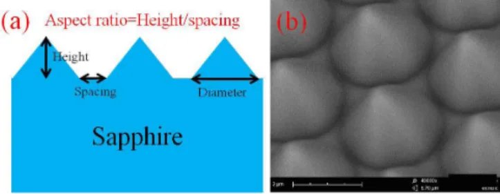
Fig. 1. (a) Illustration of the PSS for the definition of aspect ratio. (b) SEM image of HARPSS.
only increases the aspect ratio (i.e., pattern height divided by interval spacing between adjacent patterns) of PSS, as shown in Fig. 1(a), but also increases the light scattering area per chip device, thereby enhancing the LEE. The general aspect ratios of PSS are < 3 [4]–[9]. In this paper, we prepared high-aspect ratio patterned sapphire substrate (HARPSS) with an aspect ratio of 8, as shown in Fig. 1(b). The pattern height, spacing, and diameter of the HARPSS were 1.6, 0.2, and 2.8μm, respectively. The unpatterned (i.e., c-plane) area ratio of HARPSS is 21%. In other word, the area ratio of cone protrusion on the sapphire substrate is 79%. Although HARPSS could enhance the efficiency of LEDs, GaN grown heteroepitaxially on HARPSS becomes more difficult as reduc-ing area of the c-plane sapphire region. Another way to improve GaN heteroepitaxially grown on HARPSS is to take advantage of the sputtered physical vapor deposition (PVD) nucleation layer [10], [11]. Lee et al. [10] and Yen et al. [11] reported that high-quality GaN epitaxial layer prepared on sapphire substrate could be obtained by applying the PVD nucleation layer. In this paper, we introduce the PVD AlN nucleation layer into the HARPSS to reduce the dislocations of GaN epitaxial film while preserving the advantages in the LEE of HARPSS. We also report the fabrication of GaN-based LEDs using HARPSS. Detailed correlation between crystal structure and electro-optical properties of the fabricated LEDs is also discussed.
II. EXPERIMENT
The unintentionally doped GaN (uGaN) epitaxial layers grown on HARPSS with conventional metal organic chemical vapor deposition (MOCVD)-grown AlN nucleation layer (i.e.,
0018-9383 © 2014 IEEE. Personal use is permitted, but republication/redistribution requires IEEE permission. See http://www.ieee.org/publications_standards/publications/rights/index.html for more information.
Fig. 2. SEM images of GaN epitaxial layer grown on HARPSS. (a) and (b) with conventional MOCVD-grown AlN nucleation layer, (c) and (d) with PVD AlN nucleation layer in 20 mins growth time. (a) and (c) were top view SEM images. (b) and (d) were the cross sectional SEM images. The inset of Fig. 2(b) is enlarged SEM image of Fig. 2(b).
GaN I) and with the PVD AlN nucleation layer (i.e., GaN II) were both prepared via MOCVD. The detailed conventional MOCVD-grown AlN nucleation layer, PVD AlN nucleation layer, and growth procedure of uGaN were described pre-viously [11], [12]. The surface morphologies and crystal properties of these GaN epitaxial layers were then investigated through scanning electron microscopy (SEM), double-crystal X-ray diffractometry (Bede D1), and transmission electron microscopy (TEM). The electrical properties of the GaN epitaxial layers were studied via Hall effect measurements (Accent HL5550) using the van der Pauw configuration in a magnetic field of 0.5 T at room temperature. The struc-tures of the proposed LEDs on HARPSS consisted of an AlN nucleation layer, a uGaN layer, a Si-doped GaN layer, an InGaN-GaN multiple quantum well active region, an Mg-doped AlGaN cladding layer, and an Mg-doped GaN layer. The fabricated LED chip size was 300 μm × 300 μm. The detailed growth procedure of the LEDs and chip process was described in [13].
III. RESULTS ANDDISCUSSION
Fig. 2 shows the surface morphology of GaN grown on HARPSS with various AlN nucleation layer for growth time of 20 min. With conventional MOCVD-grown AlN nucleation layer [Fig. 2(a) and (b)], the GaN both grown on the c-plane region and cone region. The coalescence of laterally overgrown GaN in c-plane region and cone region occurred. However, as shown in Fig. 2(c) and (d), the growth behavior of GaN with PVD AlN nucleation layer was significantly differ-ent. The GaN grew on c-plane region rather than on the cone region. Based on these observations, it was inferred that the PVD AlN nucleation layer provided uniform nucleation layer thickness, which not only suppressed lateral growth from the cone region, but also increased vertical growth from c-plane region.
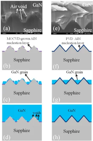
Fig. 3. Cross-sectional SEM images of GaN epitaxial layer grown on HARPSS and schematic diagram of GaN epi-layer growth mechanism. (a)–(d) with conventional MOCVD-grown AlN nucleation layer. (e)–(h) with PVD AlN nucleation layer.
Fig. 3(a) and (e) shows a cross-sectional SEM image of the GaN I and GaN II, respectively. Irregular voids are observed near the interface of the GaN epitaxial layer and cone regions of HARPSS in the GaN I. Based on the SEM images, a schematic of GaN growth behavior on HARPSS was constructed (Fig. 3) that plotted the GaN growth mode on HARPSS with different AlN nucleation layer. Fig. 3(b) shows the MOCVD grown AlN nucleation layer was deposited on the HARPSS. As shown in Fig. 3(c), the GaN grains initially both grew on the c-plane region and cone region of HARPSS at the same time. Finally, the coalescence in the c-plane region growth and cone region growth occurred, and the flat GaN epitaxial layer was obtained. A similar growth mode of GaN with MOCVD-grown nucleation layer is close to those reported in [14]. Since the different of growth rate and orientation of GaN, the irregular voids were created during the coalescence in the c-plane region growth and cone region growth. Therefore, the growth evolution of the voids in GaN prepared on HARPSS can be schematically shown in Fig. 3(b)–(d). Pan et al. [15] have described the similar forma-tion of voids in GaN grown on PSS. In addiforma-tion, GaN II was not revealed the voids. The growth mechanism of GaN with PVD AlN nucleation layer is totally different, compared with GaN with conventional MOCVD-grown AlN nucleation layer. It is attributed that the GaN epilayer was first grown onto
CHANG et al.: SPATIAL CORRELATION BETWEEN EFFICIENCY AND CRYSTAL STRUCTURE 2445
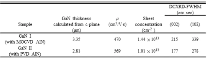
TABLE I
GaN THICKNESS, RT MOBILITY, SHEETCONCENTRATION,ANDFWHM
OFω–ROCKINGCURVES OFSAMPLES
c-plane region (i.e., the spacing region) grew using the uniform PVD AlN nucleation layer, as shown in Fig. 3(f). Then, GaN growth rate on the c-plane region is much faster than on cone region of pattern, as shown in Figs. 2(c), (d) and 3(g). Finally, GaN was overgrown into a flat film. On the other hand, the PVD AlN nucleation layer not only enhanced vertical growth on the c-plane region, but also suppressed lateral growth from the cone surface region. Therefore, no voids were observed in the GaN/sapphire interface in GaN II.
The X-ray and Hall measurements of GaN I and GaN II are presented in Table I. The TD becomes negatively charged and a space charge is formed around it, which scatters elec-trons traveling across the dislocation, thereby reducing the mobility and increasing the background concentration [16]. Table I shows the relationship between the mobility and back-ground concentration of GaN. Higher electron mobility and lower background carrier concentration can be achieved for GaN with the PVD AlN nucleation layer than those for GaN with the conventional AlN nucleation layer. In wurtzite GaN films, the full-width at half-maximum (FWHM) of the (002) ω-rocking curve is associated with the density of screw or mix dislocations, whereas the FWHM of the (102)ω-rocking curve is affected by all dislocations [17]. As shown in Table I, the FWHMs of both the (002) and (102) ω-rocking curves decrease when the PVD AlN nucleation layer is used. This result suggests that the PVD AlN nucleation layer effectively reduces the edge and mix dislocation density in the GaN epitaxial layer grown on HARPSS.
The nature of GaN crystal quality was analyzed via TEM. Fig. 4(a) and (b) shows TEM pictures of the GaN I and GaN II, respectively. As indicated by these TEM figures, the number of TD density observed from GaN II is significantly smaller than that observed from GaN I. Such an observation indicates that we can effectively suppress the value of TD density in GaN prepared on HARPSS using the PVD AlN nucleation layer. To verify the crystal structure of GaN on the c-plane sapphire region and on the cone surface region in HARPSS, the selected area diffraction (SAD) patterns were obtained from GaN I and GaN II. According to the SAD patterns, two types of GaN crystal structure were observed on GaN grown on HARPSS, as shown in Fig. 4(c)–(f). The wurtzite structure is the most common crystal structure of the GaN epitaxial layer prepared on the c-plane sapphire substrate. The other was zinc blend structure. The GaN crystal structures from the cone surfaces of HARPSS in the GaN epitaxial layer with two types of nucleation layer were significantly different. The zinc
Fig. 4. Bright-field TEM images of GaN epitaxial layer grown on HARPSS with (a) conventional MOCVD-grown AlN nucleation layer and (b) PVD AlN nucleation layer. (c) and (d) SAD patterns obtained from (a). (e) and (f) SAD patterns obtained from (b).
blend structure was observed on the cone region of HARPSS using the conventional MOCVD-grown AlN nucleation layer. In addition, TDs were generated above the zinc blend region propagated vertically to the GaN surface. Such observation of the GaN crystal structure on the cone region of the PSS has been reported in [18]. However, the crystal structure of the GaN epitaxial layer with the PVD AlN nucleation layer from cone surfaces of HARPSS was still wurzite. The difference of GaN crystal structure was attributed the different growth mode of GaN prepared on HARPSS with different AlN nucleation layer, as shown in Fig. 3. With MOCVD grown AlN nucleation layer, the grains were both grown on the c-plane region and cone region of HARPSS at the same time. The crystal structure of GaN grown on the c-plane region and cone region of HARPSS were wurtzite structure and zinc blend structure, respectively. With PVD AlN nucleation layer, the GaN was overgrown from c-plane region. Therefore, the single wurtzite structure grown on the HARPSS was revealed.
Improved thickness uniformity of sputtered PVD AlN nucle-ation layer provided high selective growth rate in the c-plane region compared with the cone surface region. A detailed growth mode study of GaN on HARPSS with various sputtered PVD AlN nucleation thickness layer is underway and the results will be reported separately.
Fig. 5 shows I –V characteristics of the fabricated LEDs measured at room temperature. These values were the average values measured from 30 fabricated LED chips With 20-mA
Fig. 5. I –V characteristics of fabricated LEDs measured at room temperature. Inset: reverse I –V characteristics of the fabricated LEDs.
Fig. 6. L–I characteristics of fabricated LEDs measured at room temperature. Inset: distributions of EL peak wavelength and light output power.
current injection, forward voltages were 3.20 and 3.16 V for LED I and LED II, respectively. The inset of Fig. 5 shows the reverse I –V characteristics of the fabricated LEDs. With a 20 V reverse bias, it was found that leakage currents measured from LED I and LED II were 4.9 × 10⁻⁵ A and 8.1×10⁻⁶A, respectively. The larger leakage current observed from LED I could be attributed to its worse crystal quality by using HARPSS with MOCVD grown AlN nucleation layer.
The relationship between light output power (LOP) and injected forward current (L–I ) was also measured. Fig. 6 shows measured LOP as functions of injection current for the fabricated LEDs. It should be noted that these values were the average values measured from 30 fabricated LED chips. It was also found that the LOP measured from the LED II was larger than that of the LED I. With 20-mA current injection, it was found that LOP were 11.08 and 16.37 mW for LED I and LED II, respectively. The 20-mA LOP of the LED with the PVD AlN nucleation layer was enhanced by 47.7% compared with the LED with the conventional MOCVD-grown AlN
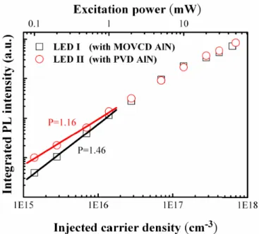
Fig. 7. Integrated PL intensity as function of injected carrier density at 300 K for both LEDs prepared on HARPSS.
nucleation layer. A significant factor in LEDs is the external quantum efficiency of LED, which is the product of the IQE and LEE. The IQE is related to the crystal quality and the LEE is associated with the geometry of LED. The LED structure and HAPSS in LED I and LED II are identical; thus, the LEE in LED I and LED II is the same. The LOP enhancement of LED II can be attributed to the IQE improvement.
To further clarify the reason for the large enhancement of IQE in the LED II, we conducted power-dependent PL mea-surements. The detailed power-dependent PL measurement procedure was described previously [19]. Fig. 7 shows the measured power-dependent efficiency as a function of injected carrier density at 300 K for LED I and LED II, respectively.
The integrated PL intensity was depicted based on the relation L ∝ IP [20], [21], where parameters L, I , and P represent the integrated PL intensity, the injected carrier density, and the power index, respectively. The P physically expresses the various recombination processes. If P equals 1, the radiative recombination principally dominates the recom-bination process. If P > 1, the nonradiative recombination process occurs. In other words, a greater increase in the value of parameter P indicates a greater increase in the nonradiative recombination process. After calculation, the fitted slopes of the integrated PL intensity (i.e., values of parameter P) for LED I and LED II are 1.46 and 1.16, respectively. The LED I exhibits a higher value of parameter P than LED II. The result reveals that the IQE of LED II is larger than that of LED I. The number of TDs in the GaN epitaxial layer on HARPSS can be reduced through the use of the PVD AlN nucleation layer, which enhances the IQE of LEDs. Such a result agrees well with that observed from DCXRD, room-temperature Hall measurement, and TEM measurement results, and again indicates that we can reduce the dislocation density via the PVD AlN nucleation layer in the GaN epitaxial layer prepared on HARPSS.
CHANG et al.: SPATIAL CORRELATION BETWEEN EFFICIENCY AND CRYSTAL STRUCTURE 2447
IV. CONCLUSION
In summary, high-quality GaN-based LED structure was successfully fabricated on HARPSS with the PVD AlN nucle-ation layer using MOCVD. We can reduce the dislocnucle-ation density to improve the material quality of the GaN epitaxial layers on HARPSS using the PVD AlN nucleation layer. In addition, the single wurtzite crystal structure in GaN on the cone surface and c-plane regions of HARPSS were obtained by employing the PVD AlN nucleation layer. The 20-mA output power of the LEDs with the PVD AlN nucleation layer was improved by 46.0% compared with that of the LEDs with the conventional MOCVD-grown AlN nucleation layer. We believe that the large light output enhancement resulted from the IQE improvement of the GaN-based LEDs prepared on HARPSS.
REFERENCES
[1] T. Mukai, M. Yamada, and S. Nakamura, “Characteristics of InGaN-based UV/blue/green/amber/red light-emitting diodes,” Jpn. J. Appl.
Phys., vol. 38, no. 7A, pp. 3976–3981, Jul. 1999.
[2] T. Mukai et al., “Recent progress of nitride-based light emitting devices,”
Phys. Status Solidi A, vol. 200, no. 1, pp. 52–57, 2003.
[3] C. H. Kuo, L. C. Chang, C. W. Kuo, and G. C. Chi, “Efficiency improve-ment of GaN-based light-emitting diode prepared on GaN nanorod template,” IEEE Photon. Technol. Lett., vol. 22, no. 4, pp. 257–259, Feb. 15, 2010.
[4] D. S. Wuu et al., “Fabrication of pyramidal patterned sapphire substrates for high-efficiency InGaN-based light emitting diodes,” J. Electrochem.
Soc., vol. 153, no. 8, pp. G765–G770, 2006.
[5] H. Y. Shin, S. K. Kwon, Y. I. Chang, M. J. Cho, and K. H. Park, “Reducing dislocation density in GaN films using a cone-shaped patterned sapphire substrate,” J. Cryst. Growth, vol. 311, no. 17, pp. 4167–4170, 2009.
[6] H. Gao, F. Yan, Y. Zhang, J. Li, Y. Zeng, and G. Wang, “Enhancement of the light output power of InGaN/GaN light-emitting diodes grown on pyramidal patterned sapphire substrates in the micro- and nanoscale,”
J. Appl. Phys., vol. 103, no. 1, pp. 014314-1–014314-5, 2008.
[7] H. C. Lin et al., “Effects of lens shape on GaN grown on microlens pat-terned sapphire substrates by metallorganic chemical vapor deposition,”
J. Electrochem. Soc., vol. 157, no. 3, pp. H304–H307, 2010.
[8] K. S. Lee et al., “Spatial correlation between optical properties and defect formation in GaN thin films laterally overgrown on cone-shaped patterned sapphire substrates,” J. Appl. Phys., vol. 107, no. 10, pp. 103506-1–103506-4, 2010.
[9] C.-C. Kao, Y.-K. Su, C.-L. Lin, and J.-J. Chen, “The aspect ratio effects on the performances of GaN-based light-emitting diodes with nanopatterned sapphire substrates,” Appl. Phys. Lett., vol. 97, no. 2, pp. 023111-1–023111-3, 2010.
[10] S. W. Lee et al., “Lattice strain in bulk GaN epilayers grown on CrN/sapphire template,” Appl. Phys. Lett., vol. 94, no. 8, pp. 082105-1–082105-3, 2009.
[11] C.-H. Yen et al., “GaN-based light-emitting diode with sputtered AlN nucleation layer,” IEEE Photon. Technol. Lett., vol. 24, no. 4, pp. 294–296, Feb. 15, 2012.
[12] C. W. Kuo et al., “Dislocation reduction in GaN with double MgxNy/AlN buffer layer by metal organic chemical vapor deposition,”
J. Cryst. Growth, vol. 311, no. 2, pp. 249–253, 2009.
[13] C. H. Kuo, L. C. Chang, C. W. Kuo, and C. J. Tun, “Improvement of the efficiency of nitride-based light emitting diodes on nanoinverted pyramid GaN templates,” J. Electrochem. Soc., vol. 156, no. 12, pp. H986–H989, 2009.
[14] M.-T. Wang, F. Brunner, K.-Y. Liao, Y.-L. Li, S. H. Tseng, and M. Weyers, “Optimization of GaN wafer bow grown on cone shaped patterned sapphire substrates,” J. Cryst. Growth, vol. 363, pp. 109–112, Jan. 2013.
[15] C.-C. Pan, C.-H. Hsieh, C.-W. Lin, and J.-I. Chyi, “Light output improvement of InGaN ultraviolet light-emitting diodes by using wet-etched stripe-patterned sapphire substrates,” J. Appl. Phys., vol. 102, no. 8, pp. 084503-1–084503-5, 2007.
[16] N. G. Weimann, L. F. Eastman, D. Doppalapudi, H. M. Ng, and T. D. Moustakas, “Scattering of electrons at threading dislocations in GaN,” J. Appl. Phys., vol. 83, no. 7, pp. 3656–3659, 1998.
[17] B. Heying et al., “Role of threading dislocation structure on the X-ray diffraction peak widths in epitaxial GaN films,” Appl. Phys. Lett., vol. 68, no. 5, pp. 643–645, Jan. 1996.
[18] Y.-C. Chen, F.-C. Hsiao, B.-W. Lin, B.-M. Wang, Y.-C. S. Wu, and W.-C. Hsu, “The formation and the plane indices of etched facets of wet etching patterned sapphire substrate,” J. Electrochem. Soc., vol. 159, no. 6, pp. D362–D366, 2012.
[19] D. W. Lin et al., “Enhanced light output power and growth mechanism of GaN-based light-emitting diodes grown on cone-shaped SiO2patterned
template,” J. Display Technol., vol. 9, no. 4, pp. 285–291, Apr. 2013. [20] I. Mártil, E. Redondo, and A. Ojeda, “Influence of defects on the
electrical and optical characteristics of blue light-emitting diodes based on III–V nitrides,” J. Appl. Phys., vol. 81, no. 5, pp. 2442–2444, 1997. [21] L. Huang, T. Yu, Z. Chen, Z. Qin, Z. Yang, and G. Zhang, “Different degradation behaviors of InGaN/GaN MQWs blue and violet LEDs,”
J. Lumin., vol. 129, no. 12, pp. 1981–1984, 2009.
Li-Chuan Chang is currently pursuing the Ph.D.
degree with the Institute of Lighting and Energy Photonics, National Chiao Tung University, Hsinchu, Taiwan.
His current research interests include nitride-based compound semiconductors and optoelectronic devices.
Yu-An Chen is currently pursuing the Ph.D. degree
with the Institute of Lighting and Energy Photonics, National Chiao Tung University, Hsinchu, Taiwan.
His current research interests include nitride-based compound semiconductors and optoelectronic devices.
Cheng-Huang Kuo is currently an Associate
Pro-fessor with the Institute of Lighting and Energy Photonics, National Chiao Tung University, Tainan, Taiwan. His current research interests include semi-conductor physics and optoelectronic devices.