國
立
交
通
大
學
資訊科學與工程研究所
碩
士
論
文
非 同 步 封 包 交 換 晶 片 網 路 : 協 定 與 架 構
Asynchronous Packet-switched Network-on-chip:
Protocol and Architecture
研 究 生:鄒柏成
指導教授:陳昌居 教授
非同步封包交換晶片網路:協定與架構
Asynchronous Packet-switched Network-on-chip:
Protocol and Architecture
研 究 生:鄒柏成 Student:Po-Cheng Tsou
指導教授:陳昌居 Advisor:Chang-Jiu Chen
國 立 交 通 大 學
資 訊 科 學 與 工 程 研 究 所
碩 士 論 文
A ThesisSubmitted to Institute of Computer Science and Engineering College of Computer Science
National Chiao Tung University in partial Fulfillment of the Requirements
for the Degree of Master
in
Computer Science
July 2010
Hsinchu, Taiwan, Republic of China
非同步封包交換晶片網路:協定與架構
研究生:鄒柏成
指導教授:陳昌居 教授
國立交通大學資訊科學與工程研究所
摘 要
最近幾年晶片上面的核心數量日益增加,而設計的複雜度也隨著核心數的增加而提 高。為了降低設計的複雜度以及提高矽智財(IP)的可重複使用性,設計者可以把數十個 先前所設計的矽智財整合在SOC上。NOC則是支援這種整合方式的連結方式。 我們提出了使用了全雙軌協定的非同步晶片網路協定去定義在IP之間的一個完全 非同步界面,提供了對使用者抽象的架構。我們同時也提出了資源網路介面 (RNI), 可 以提供IP的重複使用以及隨插即用,適用於NoC架構的多核心處理器,另外RNI也提供了 在所有的封包到達前,先將個別的封包暫存,避免單一封包的傳輸進而降低發出中斷的 次數。ii
Asynchronous Packet-switched Network-on-chip:
Protocol and Architecture
Student:Po-Cheng Tsou
Advisor:Dr. Chang-Jiu Chen
Institute of Computer Science and Engineering College of Computer Science
National Chiao Tung University
Abstract
In recent years, the number of computing resources in a single chip has been enormously increased. The complexity of design is proportional to the number of cores. In order to reduce the design complexity and increase the re-usability of the IP blocks, designers can create systems-on-a-chip (SoC) by incorporating several dozens of IP blocks which are previously designed. Network-on-Chip (NoC) has been proposed to support the integration of multiple IP blocks in a single chip.
We propose an asynchronous network-on-chips protocol (ANIP) which uses the four phase dual rail mechanism to provide an abstraction of the communication architecture. We also present a Resource Network Interface for a NoC based multiprocessor, which achieves the reuse of IP blocks, and buffers the receiving packets until all of the packets arrive to reduce the number of interruptions.
iii
Acknowledgement
這份論文的完成,最要感謝的是我的指導教授 陳昌居老師,一年多來的指導讓我 學習到許多事情,另外是兩位帶我做研究的學長 鄭緯民博士以及博士班蔡宏岳學長提 供我許多的寶貴建議以及經驗,使我能夠順利地完成本篇論文。 另外,我要感謝我父母以及家人對我的支持與關心,讓我能夠在沒有任何後顧之 憂的情況下完成學業,最後我要感謝研究所的同學們,因為你們讓我的研究所生活更 精彩。iv
CONTENTS
摘 要 ... I ABSTRACT ... II ACKNOWLEDGEMENT ... III CONTENTS ... IV LIST OF FIGURES ... VI LIST OF TABLES ... VIIICHAPTER 1 INTRODUCTION ... 1
-1.1 OVERVIEW ... -1
-1.2MOTIVATIONS ... -2
-1.3ORGANIZATION OF THIS THESIS ... -2
CHAPTER 2 BACKGROUND ... 4
-2.1ASYNCHRONOUS CIRCUITS ... -4
2.1.1 4phase dual rail protocol ... 5
2.1.2 The Muller Celement ... 7
2.1.3 The 4phase dual rail pipeline ... 8
CHAPTER 3 RELATED WORKS ... 10
-3.1BI-DIRECTION INTERCONNECTION USING TORUS TOPOLOGY ... -10
-3.2AMBAAXIPROTOCOL ... -12
3.2.1 Basic Transaction ... 13
-3.3OPEN CORE PROTOCOL ... -15
-3.4NETWORK INTERFACE ... -16
CHAPTER 4 ASYNCHRONOUS NETWORKONCHIP INTERFACE PROTOCOL ... 17
-4.1ANIP OVERVIEW ... -17
-4.2BASIC TRANSACTION ... -18
4.2.1 Read Burst ... 18
4.2.2 Write Burst ... 20
-4.3SIGNAL DESCRIPTIONS ... -21
4.3.1 Read Control Signal ... 22
4.3.2 Write Control Signal ... 23
-4.4HANDSHAKE ... -24
4.4.1 Read address phase ... 24
-v
4.4.3 Write address phase ... 26
4.4.4 Write data phase ... 28
4.4.5 Write response phase ... 29
-4.5ADDRESS OPTION ... -30
-4.6COMPARISON ... -31
CHAPTER 5 IMPLEMENTATION OF ARCHITECTURE... 32
-5.1ARCHITECTURE ... -32
-5.2IMPLEMENTATION OF THE MASTER INTERFACE ... -33
5.2.1 Read Channel ... 34
5.2.2 Write Channel ... 35
-5.3IMPLEMENTATION OF THE SLAVE INTERFACE ... -37
5.3.1 Read Channel ... 37
5.3.2 Write Channel ... 38
-5.4RESOURCE NETWORK INTERFACE ... -40
5.4.1 Request Path ... 41 5.4.2 Response Path ... 42 5.4.3 Packet Structure ... 43 5.4.5 Packet Buffer ... 44 5.4.6 FIFO Structure ... 46 CHAPTER 6 SIMULATION ... 49 -6.1TESTING ENVIRONMENT ... -49 -6.2AREA REPORT ... -51 CHAPTER 7 CONCLUSION ... 53 REFERENCES ... 54
-vi
List of Figures
FIGURE 1.1:3 X 3 NETWORK-ON-CHIPS ARCHITECTURE ... - 3 -
FIGURE 2.1 (A):4-PHASE DUAL RAIL PROTOCOL... - 6 -
FIGURE 2.1 (B):4-PHASE DUAL RAIL PROTOCOL ... - 7 -
FIGURE 2.1 (C):4-PHASE DUAL RAIL PROTOCOL... - 7 -
FIGURE 2.2:THE SYMBOL OF C-ELEMENT ... - 8 -
FIGURE 2.3 (A):TRANSISTOR LEVEL IMPLEMENTATION OF C-ELEMENT... - 8 -
FIGURE 2.3 (B):GATE LEVEL IMPLEMENTATION OF C-ELEMENT ... - 8 -
FIGURE 2.4:2 STAGE 4-PHASE DUAL RAIL PIPELINE ... - 9 -
FIGURE 2.5:THE MULTIPLE INPUTS C-ELEMENT ... - 9 -
FIGURE 3.1 : 3X3 BI-DIRECTION TORUS SYSTEM ... - 10 -
FIGURE 3.2 : PHYSICAL INTERFACE BETWEEN ROUTERS ... - 11 -
FIGURE 3.3 : PACKETS TRANSFER SEQUENCE ... - 12 -
FIGURE 3.4:AXI INTERFACE AND INTERCONNECT ... - 13 -
FIGURE 3.5:CHANNEL ARCHITECTURE ... - 14 -
FIGURE 3.6:SYSTEM SHOWING WRAPPED BUS AND OCP INSTANCES ... - 15 -
FIGURE 4.1 : SIGNALS OVERVIEW ... - 17 -
FIGURE 4.2 : READ BURST EXAMPLE ... - 19 -
FIGURE 4.3 : WRITE BURST EXAMPLE ... - 20 -
FIGURE 4.4 : READ ADDRESS TRANSACTION DEPENDENCIES ... - 24 -
FIGURE 4.5 : READ ADDRESS PHASE ... - 25 -
FIGURE 4.6 : READ DATA TRANSACTION DEPENDENCIES... - 26 -
FIGURE 4.7 : READ DATA PHASE ... - 26 -
FIGURE 4.6 : WRITE ADDRESS TRANSACTION DEPENDENCIES ... - 27 -
FIGURE 4.7 : WRITE ADDRESS PHASE ... - 27 -
FIGURE 4.8 : WRITE DATA TRANSACTION DEPENDENCIES ... - 28 -
FIGURE 4.9 : WRITE DATA PHASE ... - 28 -
vii
FIGURE 4.11 : WRITE RESPONSE PHASE ... - 30 -
FIGURE 5.1:THE OVERVIEW OF THE INTERCONNECT ... - 32 -
FIGURE 5.2:NETWORK WRAPPER ARCHITECTURE ... - 33 -
FIGURE 5.3:THE READ CHANNEL IN THE MASTER INTERFACE ... - 34 -
FIGURE 5.4:THE WRITE CHANNEL IN THE MASTER INTERFACE ... - 36 -
FIGURE 5.5:THE READ CHANNEL IN THE SLAVE INTERFACE ... - 37 -
FIGURE 5.6:THE WRITE CHANNEL IN THE SLAVE INTERFACE ... - 39 -
FIGURE 5.7:RESOURCE NETWORK INTERFACE ... - 40 -
FIGURE 5.8:DATA FLOW OF THE PACKET ASSEMBLY ... - 41 -
FIGURE 5.9:DATA FLOW OF THE PACKET REASSEMBLY ... - 42 -
FIGURE 5.10 (A):REQUEST PACKET STRUCTURE BUILT BY PACKET ASSEMBLY - 43 - FIGURE 5.10 (B):RESPONSE PACKET STRUCTURE BUILT BY PACKET ASSEMBLY- 43 - FIGURE 5.10 (C):CONTENT OF HEAD FIELD ... - 43 -
FIGURE 5.11:PACKET BUFFER FLOW CHART ... - 44 -
FIGURE 5.12:PACKET BUFFER AND PACKET TABLE ... - 45 -
FIGURE 5.13:FIFO STRUCTURE ... - 47 -
FIGURE 5.14:C-LATCH IN FIFO ... - 47 -
FIGURE 5.15:THE C-ELEMENT WITH RESET ... - 48 -
FIGURE 6.1:THE WAVEFORM OF THE READ REQUEST PHASE ... - 49 -
FIGURE 6.2:THE WAVEFORM OF THE READ RESPONSE PHASE ... - 50 -
FIGURE 6.3:THE WAVEFORM OF THE WRITE REQUEST PHASE ... - 50 -
viii
List of Tables
TABLE 2.1:1-BIT DUAL RAIL ENCODING ... - 6 -
TABLE 2.2:TRUTH TABLE OF 2-INPUT C-ELEMENT ... - 7 -
TABLE 4.1: READ CONTROL SIGNAL TABLE ... - 22 -
TABLE 4.2: MRCONTROL CONTENT ... - 22 -
TABLE 4.3: WRITE BURST SIGNAL TABLE ... - 23 -
TABLE 4.4: MWCONTROL CONTENT ... - 23 -
TABLE 4.5: SWRESP CONTENT ... - 24 -
TABLE 4.6: BURST LENGTH ENCODE ... - 30 -
TABLE 4.7: BURST TYPE ENCODE ... - 31 -
TABLE 5.1: THE DEFINITION OF PACKET FIELD ... - 43 -
TABLE 5.2: THE DEFINITION OF PACKET BUFFER AND PACKET TABLE ... - 46 -
TABLE 6.1: THE AREA OF EACH MODULE ... - 52 -
- 1 -
Chapter 1 Introduction
1.1 Overview
In recent years, the number of computing resources in a single chip has been enormously increased. The complexity of design is proportional to the number of cores. The challenge that faces the chip designers is achieving the required functionality, performance and testability whilst minimizing design cost and time to market. To achieve the goal, designers cancreate systems-on-a-chip (SoC) by incorporating several dozens of IP blocks, which are previously designed.
We can connect the IP blocks using the Network-on-chip (NoC) paradigm, because it has several advantages, for example, separation of the IP design and the functionality from chip communication and interfacing. It allows designer to use different IP blocks without worrying about the IP interfacing because the wrapper module can be used to interface the IP blocks to the network.
Asynchronous circuit design is different from the traditional synchronous circuits design, it is an emerging design. The asynchronous circuits do not have clock, where timing is managed locally, as opposed to globally with a clock in the synchronous circuit design. It has many advantages, such as power consumption, average case delay time, without the clock skew and modularity, etc. So our designs are all based on the asynchronous circuit design.
In this thesis, we present an asynchronous network-on-chips interconnect protocol (ANIP) and implement the Resource Network Interface (RNI). ANIP can be used to defines how the resources (could be processor, DSPs, memory, peripheral controller, gateway) are connected to each other in the fully asynchronous environment or the global synchronous locally asynchronous environment. The way of interconnect in the network-on-chip which adapts ANIP is arbitrarily. AMULET3i [14] adopted MARBLE [15], a fully asynchronous on-chip bus. We adopt the bi-direction Torus mechanism [9] to build the interconnection network.
- 2 -
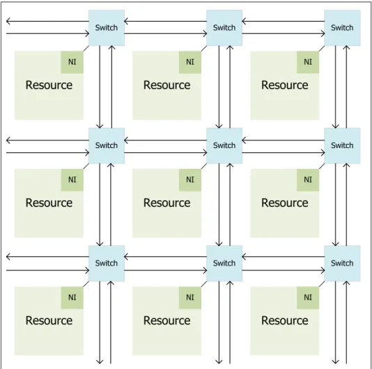
The asynchronous network-on-chips (figure 1.1) formed with the resources and the switches. A resource communicates with other resource via a network interface (NI) which converts the form of the data into the form of the packet-based communication.
1.2 Motivations
In a synchronous network-on-chip, a lot of bus protocols such as ARM AXI [10], Open Core Protocol (OPC) [11], can be adopted for the network-on-chips environment although the way of connecting each components is different from the convention. The OCP does not specify the embedded bus transfer; it is bus-independent protocol, making the IP cores independent of the architecture to achieve the goal of IP design reuse. All of these protocols are fully synchronous, and cannot be used in the asynchronous environment. Because of lack of NoC protocol in asynchronous circuit design, so we propose an AMBA AXI based asynchronous network-on-chips interface protocol (ANIP) in order to build asynchronous multicore processor in the future.
1.3 Organization of This Thesis
This thesis is organized as follow: chapter 1 is the overview of entire asynchronous network-on-chip system and the motivation. In chapter 2, we will illustrate the background about asynchronous circuit design. Chapter 3 introduce two interconnect protocol AXI and OCP which are widely used in the synchronous system interconnection, and also introduce the network interface and bi-direction interconnection using Torus Topology. Chapter 4 and 5 will discuss our design. In chapter 4, we propose the ANIP with the detailed description and the signal definition. In chapter 5, we show the implementation of the master interface, slave interface, and the resource network interface which includes a packet buffer structure to buffer the packets which received from the router to avoid transfer packet to the slave
- 3 -
interface that every packet arrive in the resource network interface. The simulation result and the conclusion are shown in chapter 6 and chapter 7.
Resource Switch Resource Switch Resource Switch Resource Switch Resource Switch Resource Switch Resource Switch Resource Switch Resource Switch NI NI NI NI NI NI NI NI NI
- 4 -
Chapter 2 Background
In this chapter, we will introduce the asynchronous circuit design methodology. Discuss the advantage and drawback of the asynchronous circuit and compare it to the synchronous circuit. Describe the function of the key component C-element in the asynchronous circuit. We also introduce the network-on-chips (NOC) in this chapter.
2.1 Asynchronous Circuits
Most of the circuits designed today are “synchronous”, which based on two
fundamental assumptions to simplify the design: (1) All the signals are binary. (2) All the components on the system share the same time domain defined by a clock signal.
The asynchronous circuits [1] [2] are different from the synchronous ones: (1) All the signals are binary too. (2) All the components on the system there is no discrete and common time, instead the circuits use the handshake between the components to perform the operation. With these differences, asynchronous circuits have several advantages which are compared with the synchronous circuits:
(1) Average case performance:
In the synchronous pipeline architecture, the cycle time of one pipeline stage must be set as the worst case of all stages. It causes the waste of the cycle time. There is no global clock in asynchronous pipeline; as a result, every stage can has its own time to finish the operation according to the type of the operation in the stage. For example, the delay of the multiplication is more than addition operation in ALU. When the operation is completed, the result is send to next stage regard less the cycle time.
(2) Low power consumption:
The sub-circuits in the synchronous circuits are clock-driven, but they are demand driven in the asynchronous circuit. Therefore the asynchronous circuits
- 5 -
do not need to consume the extra power to maintain a clock tree in the system, which at most consume 40% of power [12] in the synchronous circuits. The module actives only when it was needed in the asynchronous circuits.
(3) Better composability and modularity:
Asynchronous circuits have the better modularity resulting from the simple handshake interface and local timing. We do not care about the implementation of other part of entire system because every module of all is individual one; we just need to know the way of the handshake, input and output instead. Therefore the module which is designed using the asynchronous methodology can easily to be reused and apply to any new system.
(4) No clock distribution and clock skew problems:
There is no clock need to be distributed in the asynchronous circuits; therefore it has no clock skew problems.
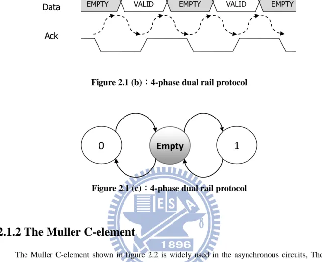
2.1.1 4-phase dual rail protocol
In the asynchronous circuits the clock is replaced by the handshake to communicate between the different components. The handshake protocol in the asynchronous circuits design is classified into 2-phase and 4-phase. In the 2-phase protocol the information is encoded as signal transition on the wires and there is no difference between a 1→0 and the 0→1 transition, they both represent a signal event. The 4-pahse protocol must return to zero
for every signal transition that cost unnecessary time and energy. Due to the characteristic of easy to implement, the 4-phase protocol is adopted constantly, like the asynchronous processor AMULET [13] and its successor, AMULET2e, AMULET3, AMULET3i [14], which are developed by the University of Manchester.
The 4-phase dual rail protocol encodes the request signal into data signals using 2 wires per bit. Figure 2.1 (a) shows the n-bit data and request signal are encoded into 2n-bit
- 6 -
data. The sender pushes the data to the receiver without signaling the request, when the receiver detect that the valid data arrives, it will signal the ack to the sender.
Figure 2.1 (a):4-phase dual rail protocol
The 1-bit data is represented by data.t and data.f shown in table 2.1. Data.t is used to signal the logic 1 (true) and data.f is used for signaling the logic 0 (false). (data.t, data.f) = (1, 0) or (0, 1) represent the valid data 1 and 0. (data.t, data.f) = (0, 0) represent the “no data” or “empty”. We can detect the valid data by observing one of two wires was asserted. In order to tell from the different phase of valid data, the empty token is needed to separate the two valid data, which is shown in figure 2.1 (c), the sequence of the data is always Valid(0/1), Empty, Valid(0/1), Empty, and so on. In figure 2.1 (b), illustrated how the 4-phase dual rail protocol work.
Value data.t data.f
EMPTY 0 0
VALID 0 0 1
VALID 1 1 0
Not used 1 1
Table 2.1:1-bit dual rail encoding 2n Data
Receiver Sender
Push channel
- 7 -
Figure 2.1 (b):4-phase dual rail protocol
Figure 2.1 (c):4-phase dual rail protocol
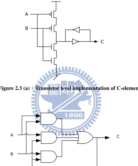
2.1.2 The Muller C-element
The Muller C-element shown in figure 2.2 is widely used in the asynchronous circuits, The
truth table of the C-element list in the table 2.2. When the value of 2 inputs A and B are both 0 (1),
the output value will change to 0 (1). The value of the output C will remain the same if the value of
input A and input B are (1,0) or (0,1). Figure 2.3 (a) and the figure 2.3 (b) show the transistor level
and the gate level implementation of the C-element respectively.
A B C
0 0 0
0 1 No change
1 0 No chande
1 1 1
Table 2.2:Truth table of 2-input C-element
EMPTY VALID EMPTY VALID EMPTY
Encoding Data Ack
1
Empty
0
- 8 -
C
A
B C
Figure 2.2:The symbol of C-element
C A
B
Figure 2.3 (a):Transistor level implementation of C-element
A
B
C
Figure 2.3 (b):Gate level implementation of C-element
2.1.3 The 4-phase dual rail pipeline
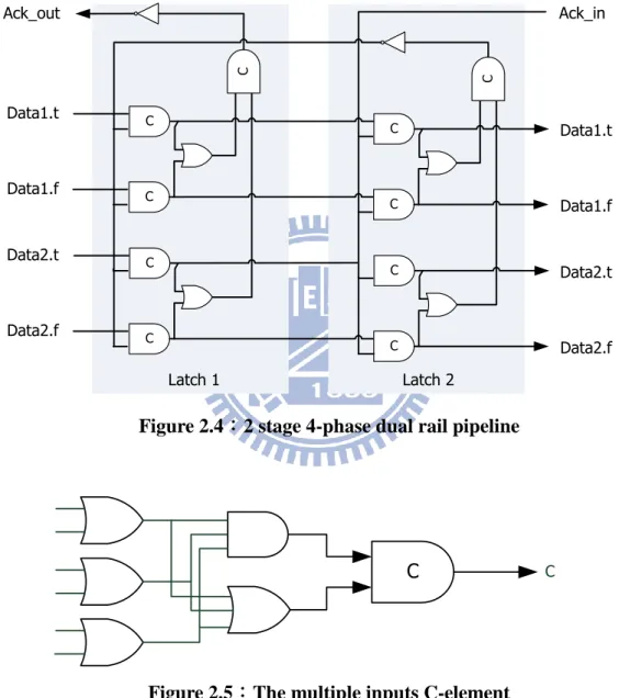
The 4-phase dual rail pipeline is based on Muller pipeline [1]. Figure 2.4 shows the two stages
dual rail pipeline with 2-bit data which is built from C-element and the inverters. After all the
C-element initialized to 0, the first data is send to the latch 1 to begin the handshake. When data
- 9 -
C-element, and then acknowledge the previous stage to complete the handshake. Figure 2.5 shows
the alternative of multiple inputs C-element which is used in the many bits complete detection units.
Because two consecutive valid data are separated by an empty token (no data), therefore the
utilization of the 4-phase dual rail pipeline is 50%.
C C C C C C C C C C Latch 1 Latch 2 Ack_in Data1.t Data1.f Data2.t Data2.f Data1.t Data1.f Data2.t Data2.f Ack_out
Figure 2.4:2 stage 4-phase dual rail pipeline
C C
- 10 -
Chapter 3 Related Works
In this chapter we will discuss the bi-direction torus system in which we used and introduce two synchronous bus protocols, ARM AXI protocol and Open Core Protocol. We also talk about the Network Interface which acts as the bus wrapper to make the interconnection details transparent to the IP core designer.
3.1 Bi-direction Interconnection using Torus Topology
Tsai proposed asynchronous bi-direction interconnection using Torus Topology [9] (figure 3.1) in NCTU, 2009. The Torus system is good for the network-on-chips interconnection because it is easy to design due to each router is the same and the torus system has a small average data path [9]. The interconnection network uses dual rail encoding (figure 3.2) and packet-switching in the torus system.(0,2) Switch (0,1) Switch (0,0) Switch (1,2) Switch (2,2) Switch (1,1) Switch (2,1) Switch (1,0) Switch (2,0) Switch NI NI NI NI NI NI NI NI NI
- 11 - Router Router Data_out.t Data_out.t Data_out.f Data_out.f Data_in.f Data_in.t Data_in.f Data_in.t Ack_in Ack_in Ack_out Ack_out
Figure 3.2 : Physical Interface between routers
Figure 3.3 shows the example of the routing protocol of the system. The router whose ID is (2,2) want to transfer one or more packets to router (0,0). The transfer will occur as follow:
(1) In the beginning the resource (2,2) send the packet to the corresponding router. (2) The router determined that whether the receiving packet has reached the
destination. If so, send the packet to the corresponding resource; otherwise put the packet to the output FIFO.
(3) The router will use the XY algorithm [9] to determine which port to which send the packet. First the router check the X-coordinate of the destination of the packet, if the destination is on the right (left) side of current router, the packet will be sent to the right (left) output port. If the destination of the packet and current router has the same coordinate, then the router compare the Y-coordinate of the destination with the Y-coordinate of current position.
Therefore packets to which router (2, 2) send will be transferred through router (3, 2), router (0, 2), router (0, 1) and router (0, 0). Each packet in this torus system has one and only one routing path.
- 12 -
Figure 3.3 : Packets transfer sequence
3.2 AMBA AXI Protocol
ARM introduced AMBA AXI protocol for high-frequency SoC design [10] in 2003, the key features of the AXI protocol that we focus on are:
1. Separate address/control and data phases
2. Burst-based transactions which only start address issue 3. Out-of –order transaction completion
4. Separate write and read data channel
In the Figure 3.4, there are several resources on the system marked as Master1 to Master3, and Slave1 to Slave3. They are connected together through some form of interconnect. At first, the master asserted the request signal of read/write, and then the interface converts the request into the format which is suitable for the interconnection definition. When the request signal arrive at the interface between the Slave and the interconnect, it will be converted to the form of the AXI protocol, and be passed to the Slave. So the designer can design the system regard less of the detail of the interconnection.
(0,3) (1,3) (2,3) (3,3)
(0,2) (1,2) (2,2) (3,2)
(0,1) (1,1) (2,1) (3,1)
- 13 -
Master 1 Master 2 Master 3
Slave 1 Slave 2 Slave 3 Interconnect
Interface Interface Interface Interface
Figure 3.4:AXI Interface and Interconnect
3.2.1 Basic Transaction
The AXI protocol is burst-based. Each transaction has the information about the control and the address either on the read address channel or the write address channel which is shown in figure 3.5. It can be one or more data transfer in a burst, which is defined by the burst length of the control information. The burst length is coupled with the burst type information, details how the address for each transfer within the burst is calculated. We will discuss the burst type in detail in the chapter 4.
In the read burst, when the data arrive on the read data channel, the data accompanies the data ID which is used to identify a transaction to which the data belong. The transactions which are the same ID must be completed in the same order. For example, at first the master issue a read request with ID 0001 to read the data memory, then the master issue a write burst with ID 0001 to write to the same data memory. The first read request must complete before the second write request to ensure the accuracy of the data. The transaction with different ID can complete out-of-order whether read or write transaction is.
AXI protocol is a kind of synchronous bus protocol, must operate in synchronization environment. All actions are positive edge trigger. It means that in the asynchronous environment, the AXI protocol does not apply. We must overcome the situation which the difficulties encountered without the clock, i.e. the signal of the AXI protocol like AWVALID is useless, because there is no clock in the asynchronous environment, so we cannot sure the
- 14 -
AWVALID and the AWADDR are arrive at the same time, and we do not know how long between the slave interface acknowledge the master and slave receive the AWVALID. So we present the Asynchronous Network-on-chip interface protocol (ANIP) to solve this problem. We will introduce ANIP in the chapter 4.
In the write burst, first of all the master interface issue an address and control information of the write operation, then the slave interface acknowledge the master interface that had received the write address. When the master has received Ack signal from the slave, the master starts to transfer the data into the data channel. At last the response information will be sent from the slave to the master that details the state of the write operation.
Master
Interface InterfaceSlave
Address & Control
Read
Data ReadData ReadData
Read Address and Control
Read Data
Address & Control
Write
Data WriteData WriteData
Write Address and Control
Write Data
Write Response
- 15 -
3.3 Open Core Protocol
The Open Core Protocol [11] defines a bus-independent interface between two communicating entities, such as IP cores and bus interface modules (bus wrapper) shown in figure 3.6, the characteristic of the IP core determined what interface do they need (Master/ Slave). The transfer occur with the system initiator issue a request (via a Master interface), and the bus wrapper interface module act as the complementary side of the OCP (Slave interface) to convert the request to the on-chip bus transfer. The receiving bus wrapper converts the on-chip bus operation into the OCP command; then the OCP master interface will transaction with the system target (via a Slave interface). The OCP does not specify the functionality of the on-chip bus, the bus initiator/target are designed by the interface designer. This increases the reusability and the modularity, we adopted the system model in our architecture design for these reasons.
Figure 3.6:System showing Wrapped Bus and OCP instances
Core Core Core
Master Master Slave Slave
Slave Slave Master Master
Bus Initiator Bus Initiator/Target Bus Target
On-chip Bus
System Initiator System Initiator / Target System Target
OCP
Bus Wrapper Interface
- 16 -
3.4 Network Interface
In NoC [3][4][5], the reuse of the IP blocks can be achieved by using a network interface, reducing the design complexity and the design time. The network interface provides a abstraction of communication architecture. The details of the interconnection are transparent to the IP designers, and make the design of new system simple.
There are many implementation of the network interface [6][7]. The main purpose of network interface is translating packet-based communication into a higher level protocol that is required by the IP, and decoupling of computation from communication.
We can classify IP blocks into two categories [6]: master (active) and slave (passive) IP blocks. Only the master can initiate a data transfer and the slave IP blocks respond to requests from the master IP blocks. Therefore the design of the master network interface is more complex than the slave network interface.
- 17 -
Chapter 4 Asynchronous Network-on-Chip
Interface Protocol
In chapter 3, two synchronous protocols are introduced. In this chapter we will propose a asynchronous network-on-chip interface protocol (ANIP) and describe the difference between ANIP and the synchronous protocols in detail.
4.1 ANIP overview
Figure 4.1: Signals overview
Ma
st
er
In
ter
face
Sla
ve In
ter
face
MRCONTROL MRADDR MRREADY SRAREADY SRDATA SRTAG SRLAST MWCONTROL MWADDR MWDATA MWDID MWLAST SWAREADY SWREADY SWRESPRead Burst
Write Burst
SWRID MWRESP- 18 -
Asynchronous Network-on-Chip Interface Protocol (ANIP) defines an asynchronous bus protocol [8] used in the network-on-chip environment. The characteristics of the ANIP are:
Burst-based protocol, every transaction has the address of the first 4-bytes in the
transfer and the control information that describes the nature of the data to be transferred.
Support the out-of-order transaction, the transaction with the same ID must be
completed in the order of issue; and the transaction with the different ID tag can be completed out of order.
Separating the address channel and the data channel, enable the master issue the
read/write address request paralleled the read/write data transfer.
Clock less protocol, unlike the synchronous protocol that all the transfer occurs in
the positive edge trigger, the ANIP handshake using the four phase dual rail mechanism.
Figure 4.1 shows the signal description of the ANIP. The definition of signals is in the chapter 4.3. The signals in ANIP can be divided into 2 groups: read burst and write burst, the transaction of read and write will describe in next section.
4.2 Basic Transaction
4.2.1 Read Burst
Figure 4.2 shows the example of the read burst, which has 2 data transfer in each read request. In this example, the master issue the read address and the control information, and the slave receive the address and control information by complete detection unit which described earlier in chapter 2 (figure 2.5).
After the master issues a read address MRADDR (Addr A) along with the control information MRCONTROL (Control A) in dual rail format on the address channel, the
- 19 -
slave accepts the address and control information, then acknowledges to the master by asserting the signal SRAREADY to 1. It means that it have received the address information. When the read data arrive, the slave will put the data on the data channel SRDATA (validA (1)) and SRTAG (IDTag A (1)) in dual rail, the complete detection unit of the master will detect the data which is arrival, then acknowledge the slave by asserting MRREADY. The SRTAG signal is the identity information of the read data. In this example what has two data transfer, so the empty token (no data) follows the valid data “ValidA (1)” after the slave accepted the acknowledgement signal MRREADY. When the
master received the empty token the MRREADY signal will go empty, and then the slave detect the MRREADY which becomes empty and put the second data on the data bus (ValidA (2) and IDTag A (2)) In this case the “ValidA (2)” is the last data transfer of the read burst A, therefore the SRLAST signal is asserted to high by the slave. After the master accepts the data (ValidA (2)) and the SRLAST, the read burst A is complete.
In this example (figure 4.2) shows that the master can drive another read burst transaction after the slave accepts the first address and control information. This property enables the slave to process the first read data in parallel with the second read burst address phase. MRCONTROL MRADDR SRAREADY SRDATA MRREADY SRLAST SRTAG Control A Addr A Control B Addr B ValidA (1) IDTag A(1) ValidA (2) IDTag A(2) ValidB (1) IDTag B(1) ValidB (2) IDTag B(2)
- 20 -
4.2.2 Write Burst
Figure 4.3 shows the example of the write burst. At the first the master put the write data address MWADDR (Addr A) and the control information MWCONTROL (Control A) on the write address channel. When the slave accepts the write address information by the complete detection unit, it acknowledge to the master by asserting the SWAREADY signal. After receiving the acknowledgement from the slave, the master put the write data MWDATA (Valid A (1)) coupled with the identity information MWDID (IDTag (1)) on the write data channel. The slave accepts the valid data then acknowledge to the master by asserting the SWREADY signal, follow by an empty token.
MWCONTROL MWADDR SWAREADY MWDATA SWREADY MWLAST SWRESP MWRESP MWDATA SWRID Control A Addr A ValidA (1) ValidA (2) IDTag (1) IDTag (2) OK ID Tag
- 21 -
When the master sends the last write data to the slave, the MWLAST signal goes high to indicate that the data is the last one. After the slave accepts the last data, the slave drives the write response signal SWRESP (OK) goes high coupled with the SWID (ID Tag), which indicates that the transaction is complete. At the last the master acknowledge to the slave by asserting the MWRESP, all the write burst is complete.
In ANIP, the address phase of the second write burst can be processed in parallel with the first write data processing. The master can issue the second write request after accepts the SWAREADY signal and put the second write request on the address channel until the previous SWAREADY goes empty. All signal transactions in ANIP must be abided by the rules that there must be an empty token (no data) (the gray in the signal transition diagram) between two valid data transition for the characteristic of the dual rail. Moreover, there is no low potential which representes no valid data in the synchronous bus protocol. Instead, we use the empty state (Table 2.1) (data.t and data.f are both low) to represent no data in ANIP.
4.3 Signal Descriptions
Signals are divided into two categories; read and write control signal list as follow. The MRCONTROL and MWCONTROL are composed of three sub control signals respectively list in table 4.2 and table 4.4 for clarity, and notice that the first letter of the name of the signals, the letter “M”/”S” means the signal is issued by the master/slave, the second letter of the name of the signal represented the type of transaction, and “R”/”W” means the signal is read/write burst. Moreover, the detail of the burst length (MRLEN/MWLEN) and the burst type MRBURST/MWBURST will be described in chapter 4.5 (Address option)
- 22 -
4.3.1 Read Control Signal
Signal Source Description
MRCONTROL[9:0] Master Read control signal information, which include the MRID, MRLEN, BRBURST information list in Table 4.2.
MRADDR[31:0] Master Read address information, coupled with the
MRCONTROL, every read burst the MRADDR must has corresponding MRCONTROL.
MRREADY Master Read acknowledgement for every data had been read by Master, Asserted when the completion of reading data SRAREADY Slave Acknowledge to Master for completion of reading
address by Slave
SRDATA[31:0] Slave Read data in the read burst
SRTAG[3:0] Slave Read data identification tag for the corresponding request of Master
SRLAST Slave Indicate the data being transfer is the last one, coupled with the last data transfer.
Table 4.1: Read Control Signal Table
MRCONTROL
Signal Description
MRID [9:6] Read address ID. This signal is the identification tag for the read address MRLEN[5:2] Read data length, from 1 to 16
MRBURST[1:0] Read Burst Type. Fixed, Increment, or Wraps, describe in detail in 4.5
- 23 -
4.3.2 Write Control Signal
Signal Source Description
MWCONTROL[9:0] Master Write control signal information, which include the MWID, MWLEN, BWBURST information list in Table 4.4.
MWADDR[31:0] Master Write address, coupled with the MWCONTROL, every write burst the MWADDR must has corresponding MRCONTROL.
MWDATA[31:0] Master Write data which Master put on the write data channel MWDID[3:0] Master Write data identification tag for the corresponding write
data, coupled with MWDATA.
MWLAST Master Indicate the last data transaction, coupled with the last data transfer of write.
MWRESP Master Acknowledge the SWRESP
SWAREADY Slave Acknowledge the Master for the write address has been read by Slave
SWREADY Slave Acknowledge to the Master for the write data has been receipt by Slave
SWRESP[1:0] Slave Acknowledge to Master that the entire write operation with the same ID has been completed
SWRID[3:0] Slave Write Response identification tag, coupled with SWRESP.
Table 4.3: Write Burst Signal Table
MWCONTROL
Signal Description
MWID [9:6] Write address ID. This signal is the identification tag for the read address MWLEN[5:2] Write data length, from 1 to 16
MWBURST[1:0] Write Burst Type. Fixed, Increment, or Wraps, describe in detail in 4.5
- 24 -
SWRESP[1:0] Description
2’b00 Write operation complete
2’b01 Write Error
2’b10 Reserved
2’b11 Reserved
Table 4.5: SWRESP content
4.4 Handshake
The handshake process can be divided into three parts, address phase, data phase and the response phase. All of these signals encoded to the dual rail form and the default value of each signal is empty (Not low). Every two consecutive valid data are separated by an empty token (no data). The slave uses the complete detection unit to detect the data arriving and
acknowledge to the slave.
4.4.1 Read address phase
The master issue a read data request by asserting the MRADDR and MRCONTROL signal. The MRADDR and MRCONTROL must remain asserted until the slave drive the SRAREADY signal high.
Figure 4.4: Read address transaction dependencies
MRADDR + MRCONTROL +
SRAREADY +
MRADDR - MRCONTROL -
- 25 -
Figure 4.5: Read address phase
Figure 4.4 shows the read address transaction dependencies, noticed that the MRADDR + and MRCONTROL – means the signals become empty (both d.t and d.f goes low). When the master detect the SRAREADY signals are driven to high, it indicates that the slave has accepted the read address and the control information, then the master drives the MRADDR and MRCONTROL to the empty. When the empty token detected by the slave’s complete detection units, the slave will let the SRAREADY signal become empty to complete the address phase transaction.
Figure 4.5 shows the address phase transaction of the read burst. When the SRAREADY signal goes high means the slave has accepted the address and control information, the transfer occurs when both the SRAREADY and MRADDR / MRCONTROL signals are high. The transaction complete when all of these three signals become empty from high.
4.4.2 Read data phase
During the read burst, the slave can assert the SRDATA signal when the read data associated with the SRTAG signal ready after the slave accepts the read address and control information from the master. The master asserts the MRREADY signal high to indicate that it accepts the data. Figure 4.5 shows the read data transaction dependencies. If the slave wants to transfer the last data of the same read burst transaction, the SRLAST signal will be driven to high to indicate that the data is the last one. When the master accepts the data
- 26 -
associated with the SRLAST signal, it will acknowledge to the slave by asserting the MRREADY signal to indicate that the read transaction is complete. The SRDATA must be coupled with the SRTAG to identify the read burst transaction. When both the SRDATA and SRTAG signals become empty, the slave can issue the next data transfer if the data is not the last or issue a new read burst data phase. Figure 4.7 shows the example of the read data transaction with two data. These two data with the same identification must be sent in order to make sure the correctness of the data sequence.
Figure 4.6: Read data transaction dependencies
Figure 4.7: Read data phase
4.4.3 Write address phase
In the write address phase, the master issue a write data request by asserting the MWADDR and MWCONTROL signal. The MWADDR and MWCONTROL must
SRDATA + (SRLAST +) MRREADY + SRDATA - (SRLAST -) MRREADY - SRTAG + SRTAG -
- 27 -
remain asserted until the slave drive the SWAREADY signal high. Figure 4.4 shows the read address transaction dependencies. When the master detect the SWAREADY signals are driven to high, it indicates that the slave has accepted the write address and the control information, and then the master drives the MWADDR and MWCONTROL to the empty. When the empty token is detected by the slave’s complete detection units, the slave will let the SWAREADY signal become empty to complete the address phase transaction. After the address phase of the write burst is complete, the master can begin sending the write data to the slave on the write data channel.
Figure 4.6: Write address transaction dependencies
Figure 4.7: Write address phase
Figure 4.7 shows the address phase transaction of the write burst, when the SWAREADY goes high, and it means the slave has accepted the address and control
MWADDR + MWCONTROL +
SWAREADY +
MWADDR - MWCONTROL -
- 28 -
information, the transfer occurs when both the SWAREADY and MWADDR / MWCONTROL signals are high. The transaction complete when all of these three signals become empty from high.
4.4.4 Write data phase
During the write data phase, the master can assert the MWDATA and MWDID signals when the read data ready after the slave accepts the read address and control information from the master and the master has accepted the acknowledgement SWAREADY from the slave. After the master asserts the MWDATA and MWDID, the slave drives the SWREADY signal high to indicate that it accepts the data.
Figure 4.8: Write data transaction dependencies
Figure 4.9: Write data phase
MWDATA + (MWLAST +) SWREADY + MWDATA - (MWLAST -) SWREADY - MWDID + MWDID -
- 29 -
Figure 4.8 shows the read data transaction dependencies. If the data which the master wants to transfer is the last, the MWLAST signal will be driven to high to indicate that the data is the last one data transfer of the same write burst transaction. When the slave accepts the data associated with the MWLAST signal, it will acknowledge to the master by asserting the SWREADY signal to indicate that the read transaction is complete. The MWDATA must be coupled with the MWDID to identify which of the write burst transaction. When both the MWDATA and MWDID signals become empty, the master can put the next data on the write data channel if the data is not the last or issue a new write burst data phase. Figure 4.9 shows the example of the write data transaction with two data. After the write data phase, the master is waiting the write response information from the slave.
4.4.5 Write response phase
The slave can assert the SWRESP coupled with SWRID signals when it drives a valid write data response. SWRESP and SWRID signals are remain high until the master accepts the response information and drives the MWRESP signals to indicate that the response information has been accepted by the master.
Figure 4.10: Write response transaction dependencies
SWRESP + SWRID +
MWRESP +
SWRESP - SWRID -
- 30 -
Figure 4.10 shows the write response transaction dependencies. When the slave detects the MWRESP signal goes high, the slave will put the empty token on the write data channel, then the master detects the empty token on the write data channel and let the MWRESP signal become empty state.
Figure 4.11: Write response phase
4.5 Address Option
Table 4.6 and Table 4.7 shows the address option of the ANIP. The burst length can be 1 to 16. There has three different type of burst type of the burst list in table 476. The burst size in ANIP are fixed to 4-byte (32 bits) for the compatibility and conformity reason.
MRLEN[3:0] MWLEN[3:0]
The number of the data transfers 2’b0000 1 2’b0001 2 2’b0010 3 …… …… 2’b1110 15 2’b1111 16
- 31 -
MRBURST[1:0] MWBURST[1:0]
Burst type Description
2’b00 Fixed Fixed address read/write burst, used in FIFO access
2’b01 Increase Incrementing address read/write burst for normal memory access
2’b10 Wrap Incrementing address read/write burst that wraps to a lower address at the wrap boundary, use in cache line access
2’b11 Reserved Reserved
Table 4.7: Burst type encode
4.6 Comparison
The main difference between ANIP and the synchronous bus protocol are listed below: 1. The data transfer occurs in the positive edge trigger in the synchronous protocol. If the
master issues a read request at clock cycle 1, then the slave accepts the address information and drives the acknowledgement signal high at cycle 2. The transfer will occur in the end of the second cycle. In ANIP, when the slave accepts the read address and the control information from the master, the slave drives the acknowledgement signal immediately without waiting.
2. The way to detect the arrival of the valid data in synchronous protocol is using a data valid signal such as ARVALID in AXI protocol, which indicates that the address and control information are available. In ANIP, using the dual rail encoding mechanism to encode the valid data. So we can use the complete detection unit described in chapter 2 to detect the available address and control information.
3. When the handshake process is complete in synchronous protocol, the signal goes low potential. But in ANIP, the signal becomes empty after the handshake is complete, i.e. there must be an empty token between two consecutive valid data transfer.
- 32 -
Chapter 5
Implementation of Architecture
This chapter is an overview of the design for the Resource Network Interface in the Switch side and the Master Interface in the resource (figure 5.1). In chapter 4 we have introduced the ANIP for the transaction; the ANIP is used for the transaction between the Resource Network Interface and the master interface shown in figure 5.2. There are two main function of the converter module in the RNI: first is converting the address/control and the data into packets, and then send these packets to the router; the second one is receiving the packet which is send from the router, and buffer it, when all of these packets arrive, the response path will convert these packets into the control/address information and data (in the read operation) and then send them to the slave interface.
5.1 Architecture
Resource 1 Resource 2 Resource 3
Master Slave Slave/ Master RNI Master /Slave Master RNI Slave RNI
Switch Switch Switch
Network Wrapper
ANIP
Figure 5.1:The overview of the interconnect
Figure 5.1 shows how the components connect in the system. The resource connects to the network via the associated slave/master interface, and the master/slave interface in the resource must be coupled with the slave/master interface in the switch side to act as a bus wrapper. The slave interface which act as the complementary side of the ANIP for the
- 33 -
Resource 1 is connected to a resource network interface. The resource network interface (RNI) converts the ANIP request into a network transfer, and the receiving Network Wrapper (as the master of the ANIP) will convert the network transfer into the ANIP command. The slave interface of the resource receive the data or request which from the master and take the corresponding action.
Master
Interface InterfaceSlave
Response Request RNI Network Wrapper Resource Switch
Figure 5.2:Network Wrapper Architecture
Figure 5.2 shows the architecture of the Network Wrapper and the master interface of the resource. Our design is divided into three parts: the master interface, slave interface, and the resource network interface. In the following sections, we will introduce these modules in detail.
5.2 Implementation of the Master Interface
The master interface can be divided into read and write channel. The master interface functions as a converter between the resource and the network wrapper (figure 5.2). The master converts the read/write data request into ANIP commands. In the write channel of the master interface, the data can be written to the FIFO. The FIFO in the write channel (figure 5.4) functions as a write buffer, and allows of writing the data to the FIFO right after the complete of write address phase. The read buffer in the slave interface (figure 5.3) will
- 34 -
send the read data to the resource until all of the data have arrived.
5.2.1 Read Channel
Figure 5.3 and figure 5.4 show the implementation of the ANIP master interface. Figure 5.3 is the read channel of the master interface. At the beginning, the processor (Resource) issues the address and control information on address channel in the address phase. The “Read Request” signals determine what kind of operation the request is. In this
Address.t Address.f MRADDR.t MRCONTROL.t C
Master Interface
Processor
MRADDR.f MRCONTROL.f ControlSignal.t ControlSignal.f SRAREADY C C C C Read Request ReadData.t ReadData.f SRDATA.t SRDATA.f MRREADY SRLAST Read FIFO SRTAG.t Write Addr Write control information SRTAG.f ReadACK TAG.t TAG.f C C C C C C C C C C Read Ack C C C C C C- 35 -
case, the path of read operation is selected. After the master interface accepts the read address and control information from the processor, the “Read Ack” signal is driven to high, to indicates that the signal had been receipted. When the master interface receives the read data from the slave interface, the data will be kept in the read buffer until all of data of the same ID tag have arrived. After all, the data and tag information will be sent to the processor. It is worth notice that if the read buffer is handshaking with the processor, write to the read buffer is not allowed.
5.2.2 Write Channel
Figure 5.4 shows the write channel of the master interface. The write channel is similar to the read channel. At the beginning, the processor issues the write address and control information on address channel in the address phase, and the data can be written to the FIFO immediately or right after the write request, i.e. the write request in the address phase and the operation in the data phase are able to occur in the same time. After the master interface accepts the address and control information, the master drive the “Write Addr Ack” signal high to indicate the handshake is complete. In the data phase, the master drives the “WriteData Ack” signals high after accepts the write data and control information from the processor. The FIFO here is simple five stage FIFO buffer.
When the write operation is complete, the slave acknowledges the complete by asserting SWRESP and SWRID signals. If an error occurs in the write burst, the response controller will send the interrupt signal to the processor. Otherwise, the response controller does not do anything after accepting the response information.
- 36 - Address.t Address.f MWADDR.t MWCONTROL.t
Processor
MWADDR.f MWCONTROL.f ControlSignal.t ControlSignal.f SWAREADY Read Request WriteData.t WriteData.f MWDATA.t MWDATA.f MWLAST FIFO SWRESP.t SWREADY SWRESP.f C C Interrupt to Processor MWRESP CMaster Interface
C C C C Read Addr Read control information C C C C C Write Addr AckRESP controller C C C C C WriteControl.t WriteControl.f C C C WriteData Ack C MWDID.f C SWRID.t C MWDID.t C SWRID.t C
- 37 -
5.3 Implementation of the Slave Interface
The slave interface also can be divided into read and write channel. Figure 5.5 and figure 5.6 show the read channel and the write channel respectively. The read channel handshakes with the read channel of the master interface, and the write channel handshakes with the write channel which is in the master interface.
5.3.1 Read Channel
MRADDR.t MRCONTROL.t MRADDR.f MRCONTROL.f SRAREADY SRDATA.t SRDATA.f MRREADY SRLAST SRTAG.t SRTAG.fRNI
Slave Interface
ReadADDR.t ReadCONTROL.t ReadADDR.f ReadCONTROL.f DATA FIFO C C ReadData.t ReadData.f C C C C C C AckADDR ReadTAG.t ReadTAG.f C C C C ADDR FIFO C C C C C C C C C DataACK Tag Table C- 38 -
The read channel of the slave interface plays a role in handshaking with the read channel of the master interface and resource network interface (figure 5.5). When the read address and control information are sent to the slave interface, the information will be inputted into the address FIFO, and then the slave interface drives the SRAREADY signals high to indicate that the read address and control information have been accepted.
When the read address and control information are accepted by the resource network interface, the tag information is also written to the tag table in the DATA FIFO (figure 5.5). It allows the slave interface to indicate that what burst the data belongs to and drive the SRLAST signal high when the last data is sent.
5.3.2 Write Channel
Figure 5.6 shows the write channel of the slave interface, which act as the complementary side of the ANIP for the associated master interface. In the write burst, the write channel accepts the write data from the master interface, and put it in the Write Buffer. Then the slave interface asserts the SWREADY signals to indicate that the write data has been accepted. After the master interface accepts the SWREADY signals, the empty token will be sent to the slave interface on the data channel. When the write process is complete in the target resource, the write response information will be sent back. The slave interface does nothing but sending these responses to the master.
- 39 - MWADDR.t MWCONTROL.t MWADDR.f MWCONTROL.f SWAREADY MWDATA.t MWDATA.f SWREADY MWLAST SWRESP.t MWRESP
RNI
Slave Interface
WriteADDR.t WriteCONTROL.t WriteADDR.f WriteCONTROL.f WriteData.t WriteData.f AckADDR C WriteResponse.t WriteResponse.f SWRESP.f C RESPACK C C C C C C C C ADDR FIFO Write FIFO C C C C C WDACK C C C WriteRespID.t SWRID.t C WriteRespID.f SWRID.f C MWDID.t MWDID.f C C C C C DataID.t DataID.f- 40 -
5.4 Resource Network Interface
The network wrapper consists of the ANIP interface and resource network interface (RNI) (figure 5.7). The RNI can further divided into two part, request path and response path. The request path is used to translate the ANIP command into the packet-based communication. When the response packets arrive, the response path keeps these packets in the packet buffer until all of them are available, and converts these packets into ANIP commands. Notice that there must be only one operation in a pipeline stage in asynchronous design. Sl av e In te rf ac e Request Response Send Port Receive Port Data FIFO TRANSLATION
TABLE HEADERBUILD
Packet Assembly Write Data Addr Latch FI FO Packet Buffer Packet Reassembly La tc h Control Data Flow Control La tc h Response Request Control La tc h Latch Data ID FI FO D ata F IF O Data Figure 5.7:Resource Network Interface
- 41 -
5.4.1 Request Path
The request path of the RNI builds the packet header, necker and wraps the data which the resource issues. The request path is shown in figure 5.8, which consists of a merge module, translation table, header builder, packet assembly module, and two FIFO. The translation table is for address decoding. The table receives the 32-bit target address from the ANIP slave interface and translates it into the network-on-chip address space. For example, if the target address is 0x010A, then the translation table will translate this address into address 0011 which represents the address (0, 1) of (X, Y) format in the NoC address space. Header Builder receives the address and control information and then converts them into the header and necker packets. After the necker packet which is built by the header builder is sent to the header FIFO, the acknowledge signal for the slave interface will be asserted. TRANSLATION TABLE Addr M ER G E ReadADDR WriteADDR AckRead ReadControl WriteControl AckWrite BUILD HEADER Addr Control Ack Packet Assembly Pa ck ets F IF O
Data FIFO Data
WDACK WriteData AckToFifo Packet to Router Ack Ack DataID DataID H ea de r F IF O Ack Ack (X,Y) (X,Y) Figure 5.8:Data flow of the Packet Assembly
When the packet assembly module has accepted the header and necker from the deader FIFO, and then it will extract the packet length from the control information. The packet assembly module receives the data from data FIFO and converts them according to the
- 42 -
packet length information. The request packet structure is shown in figure 5.10 (a). When all of the packets of the same ID have been sent to the packets FIFO, the acknowledge signal to head FIFO is asserted.
5.4.2 Response Path
The response path of the RNI receives the packets from the router and converts these packets into the ANIP commands. Figure 5.9 shows the details of the response path, which consists of a packet buffer, a C-latch, packet reassembly module, flow control unit and a data FIFO. Packet Reassembly C-La tc h Control Data Flow Control WriteResponse Data ID ReadTag ReadData RESPACK DataAck Data FIFO Data Ack Ack Data ID Ack WriteRespID Ack Packet Buffer Ack_out Packet
Figure 5.9:Data flow of the Packet Reassembly
The packet buffer keeps the arrival packets until all of them arrive. We will describe the detail of the packet buffer in next section. When the head packet arrives in the packet reassembly, the control information will be extracted from the header. The remaining data is transmitted to the data FIFO according to the packet length which is obtained from the head packet. The response information is accepted by the flow control unit, and then transfers the information to the slave interface of ANIP. After all the data and control information are sent to the data FIFO and flow control respectively, the packet reassembly module drive an acknowledge signal high to indicate that the operation is complete.
- 43 -
5.4.3 Packet Structure
Figure 5.10 shows the packet structure, and the table 5.1 lists the definition of the fields in the packet. The necker in the request packets are necessary, which indicates the start address of the read/write operation. The necker is omitted in the response packets.
Field Function Field Function
Tag {Initiator Address (X,Y) ,4 bits ID} Slave Address 32-bit Read/Write start address Type Packet type. OP code Data Packet payload
Burst Burst Type H Header tag
B-Length Burst Length (1~16) HEAD Destination coordinates Info User define Information Rsep Write response information
Length Payload length (0~17)
Table 5.1: The definition of packet field
Type Burst 0 26 27 31 32 39 Tag Length 4 5 Slave Address Data Header Necker Data 44 40 HEAD HEAD HEAD B-Length 24 25 21 20 Info 41 H H H Tag Tag
Figure 5.10 (a):Request Packet structure built by Packet Assembly 0 31 32 39 Tag Length 4 5 Header 44 40 HEAD Resp 41 H Info 6 7 Data
Data HEAD H Tag
Figure 5.10 (b):Response Packet structure built by Packet Assembly
X-coordinates Y-coordinates
35 34 33 32
- 44 -
5.4.5 Packet Buffer
Figure 5.9 shows that the packet buffer plays an important role in the response path of RNI. The packet buffer receives the packet from the router, and then sends the whole packets to the packet reassembly module until each packet of the same ID has arrived.
Receive Packet from the router
Header?
Buffer the Packet in an empty entry and set the value of
“Valid”to 1
YES
NO
Update the Packet Table
Modified the “Next”value pointed by“Last”in the
packet table
Output all the packet and clear the entries Complete = 1?
NO
YES
Figure 5.11:Packet buffer flow chart Figure 5.12 shows the operation of packet buffer as listed below: 1. Receive the packet from the router.
2. Find an empty slot in the packet buffer and write the data to the entry. Then set the field of valid to “1”, which indicates that this entry is occupied.
- 45 -
3. Check if the packet is header. If yes, go to the step 5.
4. Modified the field of “Next” whose address is pointed to by the “Last” in the corresponding entry in the packet table.
5. Update the entry in the packet table. If the packet is header, find an empty entry and write to it, otherwise update the field of “Last” in the corresponding entry. If the packet is the last one, set the “Complete” to 1.
6. Check if the field of “Complete” in the packet table is set to 1. If so, output all of the packets and then clear the entry in the packet buffer and the packet table.
000000 Tag Begin Data Next Valid (0,0) 000000 1 000010 0 1 1 000101 N/A Data 0 Data 1 Data 2 Packet Table Packet Buffer Complete 1 Last 000101 000001 000010 000011 000100 000101 111111 Valid 1 0 0 1 1 1 1
Figure 5.12:Packet Buffer and Packet Table
The example of the operation in the packet buffer is shown in figure 5.12. At the beginning the header of packets is inputted to the packet buffer, the header is written in the memory address 00000 as Data 0, and the “Valid” of the entry is set to 1. Because this packet is header, which will find an empty entry in the packet table and update the information: Set the “Valid” to 1, and write the (0, 0), 000000, 0, 000000 to the “Tag”,
- 46 -
“Begin”, “Complete”, “Last” respectively. When the second packet arrives, it will find an
empty entry as Data1 in the packet buffer and updates the value of “Next” to which is pointed by the field of “Last” in the corresponding entry in the packet table. Then the value of “Last” is modified to 000010. When the last packet arrives, it is written to the packet buffer in the address 000101as Data 2. The value of “Next” of Data 2 is set to 000101, and the value of “Last” in the corresponding entry in the packet table is also modified to 000101. Most important step is that set the value of “Complete” to 1, which indicate that all of the packets have arrived. In the end, all of these three data will be outputted, and the value of “Valid” will be set to 0.
Field Function
Valid The entry is Empty (0) or Valid (1) Data [31:0] The packet which include the HEAD Next [5:0] The index of the next packet
Tag [7:0] The X-Y coordinates of the source plus the ID Begin [5:0] The address of the first packet
Last [5:0] The location of the last data
Complete If the whole packets are received (1)
Table 5.2: The definition of packet buffer and packet table
5.4.6 FIFO Structure
Figure 5.13 shows the implementation of the FIFO. Every FIFO in our design has five stages. According to Muller pipeline, the utilization of the 4-phase dual rail pipeline is 50%. So the FIFO packs three data/packets at most. The detail design for each C-latch is shown in figure 5.14.
The transistor-level C-element is shown has been shown in chapter 2.1.2. An alternatively implementation of C-element in gate-level is shown in figure 5.15.
- 47 - C-La tc h Ack Ack C-La tc h C-La tc h Ack C-La tc h DATA Ack_out C-La tc h Ack
DATA DATA DATA DATA_out DATA_in
Ack_in
Figure 5.13:FIFO structure
C C C C C C C Data_1.t Data_1.f Data_2.t Data_2.f Data_n.t Data_n.f Data_1.t Data_1.f Data_2.t Data_2.f Data_n.t Data_n.f Ack_in Ack_out
- 48 -
A
B
C
Reset
- 49 -
Chapter 6 Simulation
6.1 Testing Environment
ModelSim 6.0 is used to verify the correctness of the functionality. Figure 5.16 shows the waveform of the functionality of the read request phase. Figure 5.17 shows the waveform of the read response phase. Figure 5.18 and figure 5.19 show the write request phase and write response phase respectively.
- 50 -
Figure 6.2:The waveform of the read response phase