Aluminum-nitride codoped zinc oxide films prepared
using a radio-frequency magnetron cosputtering system
Day-Shan Liua兲 and Chia-Sheng Sheu
Institute of Electro-Optical and Materials Science, National Formosa University, Huwei, Taiwan 63201, Republic of China
Ching-Ting Lee
Institute of Microelectronics, Department of Electrical Engineering, National Cheng Kung University, Tainan 701, Taiwan, Republic of China
共Received 15 February 2007; accepted 27 June 2007; published online 13 August 2007兲
Al–N codoped zinc oxide films were prepared using a radio-frequency magnetron cosputtering system at room temperature. AlN and ZnO materials were employed as the cosputtered targets. The as-deposited cosputtered films at various theoretical atomic ratios 关Al/共Al+Zn兲 at. %兴 showed n-type conductive behavior in spite of the N atoms exceeding that of the Al dopants, indicating that the N-related acceptors were still inactive. The crystalline structure was obviously correlated with the cosputtered AlN contents and eventually evolved into an amorphous structure for the Al–N codoped ZnO film at a theoretical Al doping level reaching 60%. With an adequate postannealing treatment, the N-related acceptors were effectively activated and the p-type ZnO conductive behavior achieved. The appearance of the Zn3N2 phase in the x-ray diffraction pattern of the annealed Al–N codoped ZnO film provided evidence of the nitrification of zinc ions. The redshift of the shallow level transition and the apparent suppression of the oxygen-related deep level emission investigated from the photoluminescence spectrum measured at room temperature were concluded to be influenced by the activated N-related acceptors. In addition, the activation of the N acceptors denoted as N–Zn bond and the chemical bond related to the Zn3N2crystalline structure were also observed from the associated x-ray photoelectron spectroscopy spectra. © 2007 American Institute of Physics.关DOI:10.1063/1.2768010兴
I. INTRODUCTION
Ultraviolet light-emitting diodes and laser diodes are re-quired for the full-color displays and data storage systems in the optoelectronics industry. Zinc oxide共ZnO兲 material with wide and direct band gap of 3.37 eV similar to the commer-cial GaN material is a promising next generation semicon-ductor because of its large exciton binding energy of 60 meV, much greater than that of GaN共24 meV兲 at room temperature. It becomes an attractive material for inducing stimulated emission at a low threshold voltage.1–4The fabri-cation of n- and p-type ZnO semiconductor using control-lable extrinsic doping is required to realize ZnO-based opto-electronic devices. The n-type ZnO is achieved even without intentional doping. Unfortunately, the p-type ZnO is very difficult to prepare for the self-compensation effect originat-ing from native defects as well as the limited solubility and inactivation of the acceptor dopants in the ZnO films.
Recently, several researchers have put efforts into the exploration of p-ZnO film by doping group V elements as p-type dopants such as N, P, As, and Sb.5–11Among these acceptors, nitrogen dopants with a shallow acceptor level is a promising candidate to substitute for oxygen atoms as NOin the ZnO films due to their similar ionic radius. To date, N-doped ZnO films have been prepared using various depo-sition methods such as chemical vapor depositon,5,12–14
pulsed-laser deposition,15implantation,6and sputtering tech-nology using different nitrogen sources such as N2, NH3, N2O, Zn3N2, and MMHy 共monomethyl hydrazine兲.9,16,17
However, the reliability and reproducibility in obtaining p-type ZnO:N is still controversial. Because of the chemical activity of O is higher than that of N, Zn is prone to combine with O rather than N, resulting in the N atoms being difficult to introduce into ZnO films. To solve this problem, some researches had diverted their concentration on the Zn3N2 ma-terial properties,18 and obtained p-type ZnO using thermal oxidation of Zn3N2 films.5,9,19 In recent years, p-type ZnO films were comprehensively achieved using the codoping method simultaneously using nitrogen acceptors and reactive III-group donors such as Ga–N, In–N, and Al–N dopants to increase the solubility of N atoms in the ZnO films.20–22 Compared with Ga and In atoms, Al is more suitable as reactive donors for their superior advantages such as low cost and near containment-free material as well as the supe-rior stability for the strong Al–N and Al–O bonds. ZnO p-n homojunction devices were therefore successfully prepared with Al–N codoped technology using the dc reactive magne-tron sputtering system employing a specific Zn:Al alloy metal target under N2O – O2 reactive gas ambient.23 How-ever, the above-mentioned deposition method was reported to be deeply influenced by the Zn:Al mixture target and the partial pressure of reactive N2O gas, resulting in an un-changed atomic composition of zinc to aluminum in the deposition film. To simplify the deposition parameters and a兲Author to whom correspondence should be addressed; FAX:
886-5-6329257; electronic mail: [email protected]
obtain Al–N codoped films at various Al doping levels, we propose a controllable and well-configured rf magnetron cosputtering method using the hexagonal crystalline struc-tures of the ZnO and AlN targets to prepare Al–N codoped ZnO films. The doping concentration in the ZnO films was easily controlled and derived using the cosputtered rf power on each target. To activate the N-related acceptor dopants and achieve p-type ZnO films, Al–N codoped ZnO films at a specific Al doping level were processed with an additive postannealing treatment. The related electrical and material properties of the cosputtered Al–N codoped ZnO films at various theoretical Al atomic ratios 关Al/共Al+Zn兲 at. %兴 were investigated. The activation of the N-related acceptors in the p-type ZnO film was conducted from the crystalline structure, photoluminescence characteristics, and chemical bond nature compared to that of the undoped ZnO film.
II. EXPERIMENT
The rf magnetron cosputtering system used in this study is equipped with a dual rf power supply that generated two different rf powers with synchronized phases. The configu-ration of the rf magnetron cosputtering chamber is illustrated elesewhere.24 ZnO 共purity of 99.99%兲 and AlN 共purity of 99.99%兲 materials were selected as the cosputtered targets. To deposit cosputtered films at various Al doping levels on glass and n-type Si共100兲 substrate at room temperature, the rf power supplied on AlN target was fixed at 85 W and the rf power supplied on ZnO target was controlled to vary from 46 to 410 W. The high AlN contents introduced into ZnO films was also prepared using the rf powers supplied on the AlN and ZnO targets at 150 and 40 W, respectively. The detailed cosputtered deposition conditions of the AlN–ZnO cosputtered films are given in Table I. The theoretical Al atomic ratios 关Al/共Al+Zn兲 at. %兴 introduced into the ZnO films could be evaluated from the following expression simi-lar to our previous descriptions in preparing the cosputtered indium tin oxide 共ITO兲-ZnO transparent and conductive films:25
D1⫻ A ⫻ d1
M1 :
D2⫻ A ⫻ d2
M2 = P:Q, 共1兲
where D1and D2共cm/min兲 are the deposition rates evaluated from the thickness of the undoped AlN and ZnO films pre-pared at specific rf powers, respectively; A共cm2兲 are defined as the cross-section area of the substrate surface; d1 and d2
共g/cm3兲 are related to the density of the AlN 共3.26 g/cm3兲 and ZnO 共5.66 g/cm3兲 materials. In addition, M1 and M2 共g/mol兲 are the molecular weights of the AlN and ZnO ma-terials; P and Q共mole兲 are the synthesized mole ratios of Al and Zn atoms in these cosputtered films. According to the deposition rates of the undoped ZnO and AlN films prepared at each rf power, shown in TableI, the theoretical Al atomic ratios 关Al/共Al+Zn兲 at. %兴 in the as-deposited cosputtered films were approximated to 5%, 10%, 20%, 30%, 40%, and 60%, respectively. With the aim of effectively activating the doping impurities, especially for the N-related acceptors, a postannealing treatment was carried out. The postannealing temperatures were varied in the range from 300 to 700 ° C for 30 min under nitrogen ambient. The undoped ZnO film deposited at an rf power of 321 W supplied on the ZnO target was also prepared as a standard reference. The film thickness of the cosputtered films and the undoped ZnO films before and after annealing treatments was measured using a surface profile system 共Veeco, Dektak 6M兲. The practical doping levels of Al and N in these as-deposited cosputtered films were examined using an energy dispersive x-ray spec-troscopy共EDS兲 quantitative analysis attached to a scanning electron microscope 共JEOL, JSM-5410LV兲. Resistivity, car-rier concentration, and Hall mobility were measured using the van der Pauw method with a Hall measurement system 共Ecopia, HMS-3000兲. The crystalline structures were exam-ined using x-ray diffraction共XRD兲 patterns observed from a diffractometer共Siemens, model D-500兲 using a Cu K␣ radia-tion source. Photoluminescence共PL兲 spectra were measured at room temperature using a He–Cd laser 共=325 nm兲 pumping source. The chemical bonds were analyzed using x-ray photoelectron spectroscopy 共XPS兲 with a monochro-matic Al K␣ source.
III. RESULTS AND DISCUSSIONS
The measured Al atomic ratios 关Al/共Zn+Al兲 at. %兴 in these cosputtered films 共decreased from 9.22 to 2.46 at. % with increasing rf power supplied on the ZnO target兲 con-ducted from an energy dispersive x-ray spectroscope quanti-tative analysis were much smaller than the theoretical Al doping levels, indicating that the AlN contents were difficult to incorporate into the ZnO films. The true atomic concen-tration of nitrogen to aluminum共N/Al in at. %兲 in the AlN– ZnO cosputtered films as a function of the rf cosputtered power on the ZnO target is shown in Fig. 1. The Al and N TABLE I. Detailed cosputtered deposition conditions of the AlN–ZnO cosputtered films.
Deposition parameters Conditions
Base pressure ⬍2⫻10−4Pa
Cosputtering gas ambient Argon gas Cosputtering pressure 1.33 Pa
Size of target 5 cm in diameter
rf power supplied on target Zinc oxide target: 40, 46, 76, 137, 321, and 410 W Aluminum nitrogen target: 85 and 150 W Deposition temperature Room temperature共cooled down by cooling water兲 Cosputtering film thickness 500 nm
Target-substrate distance Target center to substrate holder center: 5 cm Substrate holder rotation 72 rpm
dopants were successfully introduced in the cosputtered films 共referred as Al–N codoped ZnO films hereafter兲. The N atomic concentrations in these Al–N codoped ZnO films were found to be higher than that of the Al atomic concen-trations, especially for the films prepared at elevated cosput-tered powers on the ZnO target. Since large amounts of na-tive defects such as zinc interstitials and oxygen vacancies were reported as prone to be induced while depositing the ZnO films at higher rf powers,26 N atoms ionized from cosputtering were likely to be attracted by those Zn-rich de-fects. This brought about more N impurities introduced into the ZnO films. However, because of the soluble limitation of N in the ZnO films, the measured N atom concentrations in these cosputtered films were nearly unchanged in spite of the increased Al doping concentration. As a result, the Al atom doping concentrations in these cosputtered films were gradu-ally close to that of N atoms at lower cosputtered powers supplied on the ZnO target. The electrical property evolu-tions of these as-deposited Al–N codoped ZnO films at vari-ous theoretical Al doping levels, as well as that of an un-doped ZnO film, are illustrated in Fig. 2. Although the N impurity atomic ratios in the as-deposited cosputtered films were found to be in excess of that of the Al contents. These as-deposited Al–N codoped ZnO films still showed n-type conductive behavior. High electron carrier concentrations 共about 1018– 1019cm−3兲 were obtained from these cosput-tered films at theoretical Al atomic ratios ranging from 10% to 40%, while that of the undoped ZnO film showed a much lower electron carrier concentration. This implied that the
doping Al impurities were able to donate free electrons in the as-deposited cosputtered films whereas the N-related accep-tors were electrically inactive. As a result, an apparent in-crease in the electron carrier concentration was obtained in spite of the high N to Al atomic ratios shown in Fig.1 mea-sured in the as-deposited Al–N codoped ZnO films. Figure3
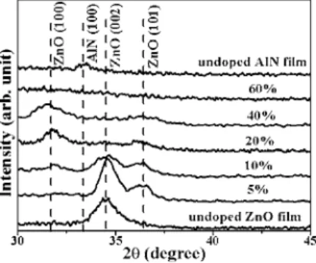
shows the crystalline structures of the as-deposited cosput-tered films as well as undoped ZnO and AlN films deposited on glass substrates. An apparent diffraction peak determined as ZnO共002兲 phase was observed from the diffraction pat-tern of the undoped ZnO film. A weak diffraction peak iden-tified as AlN共100兲 appeared in the undoped AlN film. This indicated that the preferred growth orientation of the un-doped ZnO film was distinct from the unun-doped AlN film in spite of their similar hexagonal crystalline structures. As a result, the crystalline structure was suggested to be disor-dered due to the cosputtered AlN contents introduced into the ZnO films. Indeed, the preferred orientations were gradually evolved from the ZnO共002兲 phase to ZnO 共100兲 phase with increasing the AlN contents in the ZnO films. For the cosput-tered film at a theoretical Al atomic ratio of 60%, ZnO phases were entirely absent in the diffraction pattern and it became an amorphous crystalline structure. The poor crystal-line structure was the consequence of the inferior electrical property shown in Fig. 2. So far, we succeeded in realizing Al–N codoped ZnO films from this rf magnetron cosputter-ing system uscosputter-ing ZnO and AlN targets. The N to Al atomic doping levels in the ZnO films could be simply tuned via controlling the rf powers supplied on the ZnO and AlN tar-gets. The related electrical and material properties were found to be deeply influenced by the AlN contents intro-duced into the ZnO films. However, from the view point of these cosputtered film conductive types, the incorporated N acceptor dopants in these Al–N codoped films deposited at room temperature seemed to be inactive and resulted in the n-type conductive behavior for all the produced cosputtered films. Applications in the photoelectronic devices using ZnO homojunction structures were thus limited due to the mono-tonic conductive type performance of these as-deposited Al–N codoped ZnO films. As a result, the N-related acceptor dopants should be properly activated to convert the cosput-tered film conductive type into p-type conductive behavior. Under this consideration, a postannealing treatment was car-ried out to activate these N-related acceptor dopants in the cosputtered films. For p-type ZnO codoped films with reac-FIG. 1. Atomic concentration of nitrogen to aluminum共N/Al兲 in the AlN–
ZnO cosputtered films as a function of the rf cosputtered power on ZnO target 共the theoretical Al atomic ratio 关Al/共Zn+Al兲 at. %兴 is shown in bracket兲.
FIG. 2. Film resistivity, carrier concentration, and Hall mobility of the as-deposited Al–N codoped and undoped ZnO films.
FIG. 3. X-ray diffraction patterns of the as-deposited Al–N codoped ZnO films as well as the undoped ZnO and AlN films.
tive donors and nitrogen acceptors, the reactive donors using the group III elements共III=Al, Ga, or In兲 and 2N was dem-onstrated by theoretical calculation.27As a result, a fine con-trol on the N to Al atoms doping concentration and the sup-pression of the Al contents in the ZnO film was required to accomplish p-type ZnO film preparation. According to the measured N / Al atomic ratios shown in Fig.1, the theoretical calculation of N / Al= 2 : 1 共indicated by the dashed line兲 is located between the as-deposited cosputtered films at the the-oretical Al atomic ratios of 10% and 20%. Because the mea-sured N / Al atomic ratio in the cosputtered film at a theoret-ical Al doping level of 10% was about 2.69, the p-type conduction was expected to be achieved due to the enhanced quantity of Zn–N bonds via complex N–Al–N shallow ac-ceptors formation after thermal activation treatment.28 More-over, since the activation of the NO-double-donor complexes such as NO– VO, NO– Zni, and NO– ZnOwere demonstrated to donate free electron carriers in the N-doped ZnO films,29,30the annealing temperature and atmosphere became critical issues to properly activate the N-related acceptors in the cosputtered films. As a result, they were annealed under nitrogen ambient to avoid the outdiffusion of N atoms that had been introduced into the ZnO films by cosputtering.
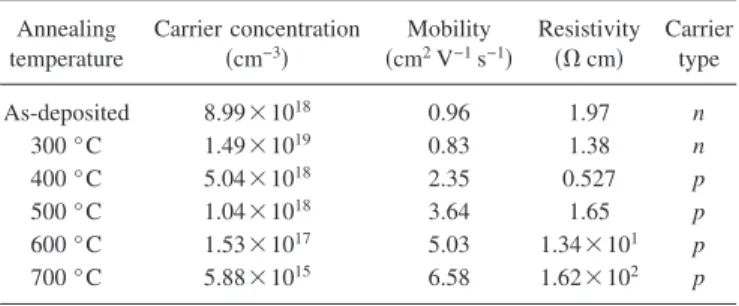
P-type ZnO conductive behavior was obtained from the cosputtered film at a theoretical Al doping level of 10% pro-cessed with an additive postannealing treatment at tempera-tures ranging from 400 to 600 ° C under nitrogen ambient for 30 min. The carrier concentration, Hall mobility, and re-sistivity of the Al–N codoped ZnO films at a theoretical Al doping level of 10% deposited onto silicon substrates after thermal annealing based on the Hall effect measurements at room temperature are summarized in TableII. At an anneal-ing temperature of 300 ° C, the Al–N codoped ZnO film per-formed n-type conduction with a slightly higher electron concentration than the as-deposited film. This indicated that the annealing temperature was too low to activate the N-related acceptors and more donors were generated. As the annealing temperature reached 400 ° C, the annealed Al–N codoped ZnO film with a hole carrier concentration of 5.04 ⫻1018cm−3, mobility of 2.35 cm2V−1s−1, and resistivity of 0.527⍀ cm was obtained, whereas that of an undoped ZnO film annealed under the same conditions showed an electron carrier concentration of 2.57⫻1017 cm−3 and Hall mobility of 5.47 cm2V−1s−1. This implied that large amounts of N-related acceptors were effectively activated and predomi-nated over the donors in the codoped film under this
anneal-ing treatment. As a result, free hole carriers were measured from the annealed Al–N codoped ZnO films. By further in-creasing the annealing temperature, more donor-related de-fects such as VOand VNwere prone to be produced, result-ing in a decrease in the hole carrier concentration. X-ray diffraction patterns for Al–N codoped and undoped ZnO film crystalline structures deposited on silicon substrates annealed at a temperature of 400 ° C are shown in Fig. 4. It can be seen that both the codoped and undoped ZnO films annealed under nitrogen ambient exhibited polycrystalline structures with the dominated diffraction peaks of ZnO共002兲 and 共101兲 phases in the associated diffraction patterns. Due to the in-fluence of Al and N impurities, the full width at half maxi-mum 共FWHM兲 of the ZnO-related diffraction peaks in the diffraction pattern of the annealed Al–N codoped ZnO film was broader than that of the undoped ZnO film. According to Scherrer’s formula, the mean crystallite size of the annealed Al–N codoped ZnO film evaluated from the FWHM of the ZnO 共002兲 phase 共⬃9.7 nm兲 was apparently smaller than that of the undoped ZnO film 共⬃17.3 nm兲 and as a conse-quence of the lower carrier mobility due to the grain bound-ary scattering. In addition, except for the ZnO-related dif-fraction peaks, a weak difdif-fraction peak determined as Zn3N2 共222兲 was observed from the annealed Al–N codoped ZnO film diffraction pattern. The appearance of the zinc nitride phase was believed to be the nitrification reaction of the ex-cess Zn and N atoms in the codoped films, indicating the excitation of the N ions after thermal annealing.
The room temperature PL spectra of the Al–N codoped and undoped ZnO films deposited on silicon substrates an-nealed at a temperature of 400 ° C are illustrated in Fig. 5. The main feature for the PL spectrum of the undoped ZnO film could be divided into three categories: the near band edge emission 共⬃3.24 eV兲, the low energy tail extending from the near band edge emission共⬃3.07 eV兲, and the deep level emission 共⬃2.11 eV兲. According to the previous re-ports, the low energy tail extending from the near band edge emission was related to the Zn-related shallow level transi-tions, whereas the oxygen-related deep level transitions were responsible for the broad green-yellow emission.31–33The PL spectrum of the annealed Al–N codoped ZnO film was obvi-ously different from that of the annealed undoped ZnO film in both emission peak structure and intensity. The FWHM of the ultraviolet emission was broader and dominated by the TABLE II. Electrical properties of the Al–N codoped ZnO films共theoretical
Al atomic ratio of 10%兲 deposited on silicon substrates annealed at various temperatures under nitrogen ambient for 30 min.
Annealing temperature Carrier concentration 共cm−3兲 Mobility 共cm2V−1s−1兲 Resistivity 共⍀ cm兲 Carrier type As-deposited 8.99⫻1018 0.96 1.97 n 300 ° C 1.49⫻1019 0.83 1.38 n 400 ° C 5.04⫻1018 2.35 0.527 p 500 ° C 1.04⫻1018 3.64 1.65 p 600 ° C 1.53⫻1017 5.03 1.34⫻101 p 700 ° C 5.88⫻1015 6.58 1.62⫻102 p
FIG. 4. X-ray diffraction patterns of the Al–N codoped 共theoretical Al atomic ratio of 10%兲 and undoped ZnO films deposited on silicon substrates annealed at a temperature of 400 ° C under nitrogen ambient for 30 min.
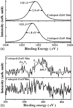
shallow defect transition with an apparent redshift of about 60 meV. The oxygen-related deep emission was suppressed and a broad blue-green emission at about 2.62 eV emerged from the PL spectrum. The blue-green emission was re-garded as the dopant-induced defects that also had been ob-served from related research in the preparation of the Al–N codoped ZnO films.33,34 Except for the defect-related emis-sion induced from the codoping process, the activated N-related acceptors in the oxygen sites共NO兲 was responsible for the redshift on the shallow level transition due to the fact that NO was recognized as shallow acceptors and sequen-tially suppressed the formation of the oxygen-related deep level emission.35 As a consequence, the annealed Al–N codoped ZnO film performed with p-type conductive behav-ior. Figures6共a兲and6共b兲show the typical XPS spectra of Zn 2p3/2and N 1s core level obtain from the Al–N codoped and undoped ZnO films deposited on silicon substrates annealed at a temperature of 400 ° C. The binding energy peak of the Zn 2p3/2 for the Al–N codoped ZnO film共1021.6 eV兲 was
higher than that of the undoped ZnO film 共1021.3 eV兲. The related FWHM of the Al–N codoped ZnO film共2.0 eV兲 was also broader than that of the undoped ZnO film共1.8 eV兲. For the Al–N codoped ZnO film, the crystalline structure was inferior to that of the undoped ZnO film due to the intro-duced N and Al dopants, as shown in Fig.4. As a result, the electrical cloud around the Zn atoms in the Al–N codoped ZnO film were prone to be asymmetrical, resulting in the increase in the binding energy of the Zn 2p3/2 core level.14,18,30,36 In addition, the broad FWHM also suggested to be contributed by the Zn–N bonds. However, since the Zn 2p3/2 peak was almost completely dominated by the Zn–O chemical bond, it was quite difficult to deconvolve the Zn–N chemical bond. Therefore, the N 1s core level signal was a preferable tool to investigate the activation of N impurities. As can be seen in Fig. 6共b兲, no obvious peak corresponding to N was observed from the undoped ZnO film, whereas that of the Al–N codoped film showed two peaks at around 395.7 and 399.7 eV. The peak at a binding energy of 395.7 eV was in agreement with XPS spectra reported on Zn3N2 thin films,18,37manifesting the crystalline structure shown in Fig.
4. In addition, the peak at a high binding energy of 399.7 eV was broad and asymmetrical with a shoulder observed on the low binding energy side. This implied that this binding en-ergy signal was composed of at least two chemical bonds. According to the previous works on nitrogen-doped and Al–N codoped ZnO films,5,14,30,38–40 the lower binding en-ergy tail was attributed to the N ions substituted for O ions recognized as N–Zn chemical bond 共indicated by NO at about 398.3 eV兲 in the ZnO lattice. The high binding energy side was denoted as the chemical state emerged from the neutrally charged N ions共⬃400 eV兲. The appearance of the N–Zn chemical bond was directly related to the activation of N acceptors and a consequence of achieving p-type ZnO conductive behavior.
IV. CONCLUSIONS
In summary, Al–N codoped ZnO films had been success-fully prepared using an rf magnetron cosputtering system at room temperature with AlN and ZnO targets. Because of the oxygen atoms deficiency in the ZnO films, the nitrogen atomic concentrations were in excess of the Al contents in the as-deposited cosputtered films, especially at low Al dop-ing levels. The conductive behavior of these as-deposited codoped Al–N films all showed n-type conduction. Regard-ing the crystalline structure evolutions, the preferred ZnO 共002兲 c-axis diffraction peak appeared in the x-ray diffraction pattern of the undoped ZnO film and gradually vanished due to AlN content introduction and domination by the ZnO 共100兲 crystalline phase with increasing the Al doping impu-rities. As the theoretical Al doping level 关Al/共Al + Zn兲 at. %兴 reached 60%, the crystalline structure of the cosputtered film evolved into an amorphous structure. The N-related acceptors in the Al–N codoped ZnO film at a the-oretical Al atomic ratio of 10% were found to be sufficiently activated with an adequate postannealing treatment. A hole carrier concentration of 5.04⫻1018cm−3, Hall mobility of 2.35 cm2V−1s−1, and film resistivity of 0.527⍀ cm was FIG. 5. Room temperature PL spectra of the Al–N codoped共theoretical Al
atomic ratio of 10%兲 and undoped ZnO films deposited on silicon substrates annealed at a temperature of 400 ° C under nitrogen ambient for 30 min.
FIG. 6. Typical XPS spectra of共a兲 Zn 2p3/2and共b兲 N 1s core level for the Al–N codoped and undoped ZnO films deposited on silicon substrates an-nealed at a temperature of 400 ° C under nitrogen ambient for 30 min.
achieved for the Al–N codoped ZnO films annealed at a tem-perature of 400 ° C under nitrogen ambient for 30 min. The Zn3N2 phase that appeared in the x-ray diffraction pattern was attributed to the nitrification of the excess zinc ions in the codoped films after thermal annealing. In addition, the redshift of the shallow level transition and oxygen-related deep level emission suppression in PL spectrum were related to the activated N-related acceptors. The chemical bond as-cribed to O atoms replaced by N impurities and the chemical nature recognized as the Zn3N2crystalline structure observed from the N 1s core level in the XPS spectra of the annealed Al–N codoped ZnO film also provided a direct evidence of the N dopant activation of and sequentially performed p-type ZnO conductive behavior. The controllable Al–N codoped ZnO film obtained from this rf magnetron cosputtering sys-tem using AlN and ZnO targets at room sys-temperature and the conversion of p-type ZnO conductive behavior with an addi-tive postannealing treatment will greatly benefit the develop-ment of ZnO-based homostructural optoelectronic devices.
ACKNOWLEDGMENT
This work was supported by the National Science Coun-cil of the Republic of China under NSC94-2218-E150-004.
1Z. K. Tang, G. K. L. Wong, P. Yu, M. Kawasaki, A. Ohtomo, H. Koinuma,
and Y. Segawa, Appl. Phys. Lett. 72, 3270共1998兲.
2A. Mitra and R. K. Thareja, J. Appl. Phys. 89, 2025共2001兲.
3Y. I. Alivov, E. V. Kalinina, A. E. Cherenkov, D. C. Look, B. M. Ataev, A.
K. Omaev, M. V. Chukichev, and D. M. Bagnall, Appl. Phys. Lett. 83, 4719共2003兲.
4W. Liu et al., Appl. Phys. Lett. 88, 092101共2006兲. 5B. S. Li et al., J. Mater. Res. 18, 8共2003兲.
6C. C. Lin, S. Y. Chen, S. Y. Cheng, and H. Y. Lee, Appl. Phys. Lett. 84,
5040共2004兲.
7D. C. Look, G. M. Renlund, R. H. Burgener II, and J. R. Sizelove, Appl.
Phys. Lett. 85, 5269共2004兲.
8V. Vaithianathan, B. T. Lee, and S. S. Kim, J. Appl. Phys. 98, 043519
共2005兲.
9Y. Nakano, T. Morikawa, T. Ohwaki, and Y. Taga, Appl. Phys. Lett. 88,
172103共2006兲.
10F. X. Xiu, Z. Yang, L. J. Mandalapu, J. L. Liu, and W. P. Beyermann,
Appl. Phys. Lett. 88, 052106共2006兲.
11Y. J. Zeng et al., Appl. Phys. Lett. 88, 262103共2006兲.
12G. Du, Y. Ma, Y. Zhang, and T. Yang, Appl. Phys. Lett. 87, 213103
共2005兲.
13J. L. Zhao, X. M. Li, J. M. Bian, W. D. Yu, and C. Y. Zhang, J. Cryst.
Growth 280, 495共2005兲.
14Z. Xiao, Y. Liu, J. Zhang, D. Zhao, Y. Lu, D. Shen, and X. Fan, Semicond.
Sci. Technol. 20, 796共2005兲.
15J. G. Lu, Y. Z. Zhang, Z. Z. Ye, L. P. Zhu, L. Wang, B. H. Zhao, and Q. L.
Liang, Appl. Phys. Lett. 88, 222114共2006兲.
16C. Wang, Z. Ji, K. Liu, Y. Xiang, and Z. Ye, J. Cryst. Growth 259, 279
共2003兲.
17M. L. Tu, Y. K. Su, and C. Y. Ma, J. Appl. Phys. 100, 053705共2006兲. 18M. Futsuhara, K. Yoshioka, and O. Takai, Thin Solid Films 322, 274
共1998兲.
19E. Kaminska et al., Phys. Status Solidi C 2, 1119共2005兲.
20A. V. Singh, R. M. Mehra, A. Wakahara, and A. Yoshida, J. Appl. Phys. 93, 396共2003兲.
21J. M. Bian, X. M. Li, X. D. Gao, W. D. Yu, and L. D. Chen, Appl. Phys.
Lett. 84, 541共2004兲.
22F. Zhuge et al., J. Cryst. Growth 268, 163共2004兲. 23F. Zhuge et al., Appl. Phys. Lett. 87, 092103共2005兲.
24D. S. Liu, C. C. Wu, and C. T. Lee, Jpn. J. Appl. Phys., Part 1 44, 5119
共2005兲.
25D. S. Liu, C. H. Lin, F. C. Tsai, and C. C. Wu, J. Vac. Sci. Technol. A 24,
694共2006兲.
26C. R. Aita, R. J. Lad, and T. C. Tisone, J. Appl. Phys. 51, 6405共1980兲. 27T. Yamamoto and H. K. Yoshida, Jpn. J. Appl. Phys., Part 2 38, L166
共1999兲.
28G. W. Cong et al., Appl. Phys. Lett. 88, 062110共2006兲.
29Y. M. Lu, W. S. Hwang, W. Y. Liu, and J. S. Yang, Mater. Chem. Phys. 72,
269共2001兲.
30E. C. Lee, Y. S. Kim, Y. G. Jin, and K. J. Chang, Phys. Rev. B 64, 085120
共2001兲.
31X. L. Wu, G. G. Siu, C. L. Fu, and H. C. Ong, Appl. Phys. Lett. 78, 2285
共2001兲.
32B. Lin, Z. Fu, Y. Jia, and G. Liao, J. Electrochem. Soc. 148, G110共2001兲. 33Y. G. Wang, S. P. Lau, H. W. Lee, S. F. Yu, B. K. Tay, X. H. Zhang, and
H. H. Hng, J. Appl. Phys. 94, 354共2003兲.
34J. G. Lu, L. P. Zhu, Z. Z. Ye, F. Zhuge, B. H. Zhao, J. Y. Huang, L. Wang,
and J. Yuan, J. Cryst. Growth 283, 413共2005兲.
35U. Ozgur et al., J. Appl. Phys. 98, 041301共2005兲.
36Y. M. Chung, C. S. Moon, M. J. Jung, and J. G. Han, Surf. Coat. Technol. 200, 936共2005兲.
37F. Zong, H. Ma, C. Xue, H. Zhuang, X. Zhang, H. Xiao, J. Ma, and F. Ji,
Solid State Commun. 132, 521共2004兲.
38H. Maki, I. Sakaguchi, N. Ohashi, S. Sekiguchi, H. Haneda, J. Tanaka, and
N. Ichinose, Jpn. J. Appl. Phys., Part 1 42, 75共2003兲.
39Y. F. Mei, R. K. Y. Fu, G. G. Siu, K. W. Wong, P. K. Chu, R. S. Wang, and
H. C. Ong, Appl. Surf. Sci. 252, 8131共2006兲.
40S. U. Yuldashev, G. N. Panin, T. W. Kang, R. A. Nusretov, and I. V.