CMOS 積體電路之金屬氮化物閘極電極研發與特性研究(2/2)
65
0
0
全文
(2) 行政院國家科學委員會補助專題研究計畫. ; 成 果 報 告 □期中進度報告. CMOS 積體電路之金屬氮化物閘極電極研發與特性研究. 計畫類別:; 個別型計畫 □ 整合型計畫 計畫編號:NSC 93-2216-E-006-015 執行期間:2003 年 08 月 01 日至 2005 年 07 月 31 日 計畫主持人:陳貞夙 計畫參與人員: 賴宜生 江佩錞 王勢輝 呂政學 蔡志煌. 成果報告類型(依經費核定清單規定繳交):□精簡報告. ;完整報告. 本成果報告包括以下應繳交之附件: □赴國外出差或研習心得報告一份 □赴大陸地區出差或研習心得報告一份 ;出席國際學術會議心得報告及發表之論文各一份 □國際合作研究計畫國外研究報告書一份. 處理方式:除產學合作研究計畫、提升產業技術及人才培育研究計畫、 列管計畫及下列情形者外,得立即公開查詢 □涉及專利或其他智慧財產權,□一年□二年後可公開查詢 執行單位:國立成功大學 中. 華. 民. 國. 94. 材料科學及工程學系 年. 10. 月. 30. 日.
(3) 摘要 隨著 CMOS 元件的閘極寬度收縮至 0.1μm 以下,為了增進元件的特性及降低短通道 效應,傳統的二氧化矽閘極氧化層的厚度必須降低至 20Å 以下。然而過薄的二氧化矽將 會由於電子電洞穿隧電流的增加,而引發高的漏電流,因而增加能量的消耗以及影響電 路的運作。傳統的 P 型多晶矽閘極電極也隨著尺寸的降低而有空乏效應以及硼穿透的現 象發生,因而降低了整體電容值以及氧化層的可靠度。為了克服超薄氧化層及多晶矽閘 極帶來的問題,必須使用高介電常數材料及新的閘極材料來延續縮小元件尺寸的趨勢。 由於傳統的多晶矽閘極電極面臨的問題,因此,金屬或金屬氮化物成為取代多晶矽 閘極電極材料的新選擇。以金屬氮化物作為閘極電極,閘極中氮的含量以及結晶結構卻 沒有詳細的研究資料。因此,本研究第一部分以不同氮含量的氮化鎢作為閘極電極,而 以二氧化矽作為閘極氧化層,研究氮含量對於氮化鎢作為閘極電極的影響。 改變氮化鎢的氮含量可以得到 WN0.6、WN0.8 和 WN1.5 三種不同成分的閘極電極,且 其功函數分別為 4.40、4.91 和 4.38 eV。經過 500oC 的退火後,WN0.6 閘極表面的化學鍵 結為 W-O 鍵,而無 W-N 鍵,且二氧化矽中的氧擴散進入閘極,因而在閘極與介電層之 間形成一層混合層,此結果造成電容器的平帶電壓往正偏壓方向偏移。然而對於高氮含 量的 WN0.8 和 WN1.5 閘極而言,在退火後,均有良好的表面抗氧化性以及沒有明顯的閘 極與介電層反應發生。在電容器的漏電行為表現上,閘極材料中氮含量的多寡對於介電 層的漏電並沒有明顯的影響。 本研究第二階段則使用結晶的五氧化二鉭(Ta2O5)為高介電常數材料,而閘極材料為 WN0.8 薄膜。藉由在不同退火氣氛(H2 與 H2+N2)及退火溫度(400-600oC)下,觀察 WN0.8 閘極的熱穩定性以及 WN0.8 閘極與 Ta2O5 氧化層界面的穩定性。研究結果顯示當退火溫 度達到 600oC,WN0.8 閘極的表面會有氧化的現象產生,主要是因為薄膜中的氮原子有向 表面逸散的現象發生,H2+N2 退火氣氛可以阻止氮原子的擴散現象。當退火溫度高達 600oC,WN0.8 閘極與 Ta2O5 氧化層仍能維持良好的穩定性。而退火溫度的提升可以降低 氧化層與基材界面的捕獲電荷數與降低氧化層漏電流之值。. 關鍵詞:氮化鎢,五氧化二鉭,閘極電極,退火氣氛。.
(4) Abstract With shrinking of complementary metal oxide semiconductor (CMOS) device dimensions to the sub-0.1 μm regime, the vertical dimension of SiO2 is also being scaled down to less than 20Å in order to obtain the high device performance and to suppress short channel effects. In the regime of SiO2 thickness, however, the large gate leakage current due to electron and hole tunneling will increase static power consumption and affect circuit operation. The p+ poly-silicon gate also occurs poly-depletion and boron penetration effects with decreasing dimensions, and those effects will decrease the capacitance and oxide layer reliability. Therefore, high dielectric constant (high-k) materials with greater thickness and new gate electrode materials must replace SiO2 and poly-silicon to overcome the obstacles associated with the small device dimension. The conventional poly-silicon gate electrode of CMOS devices suffers several problems, therefore, metals or metal nitrides will be interesting materials for gate electrode application. Nevertheless, nitrogen concentration and structure of metal nitride gate electrodes are not fully explored in previous studies. In the first part of this study, WNx and SiO2 are chosen as the gate electrode and gate dielectric of MOS capacitors, respectively. The films with composition of WN0.6, WN0.8 and WN1.5 are obtained with different nitrogen content. The work function of WN0.6, WN0.8 and WN1.5 are 4.40, 4.91 and 4.38 eV, respectively. After annealing at 500oC, the surface of the WN0.6 film reveals only the W-O bonding, but no W-N bonding. In addition, oxygen diffused from SiO2 into WN0.6 and leads to the formation of a mixing layer. Subsequently, flatband voltage (VFB) of the MOS capacitor shifts positively after annealing at 500oC. After annealing at 500oC, WN0.8 and WN1.5 films exhibit better resistance to oxidation than the WN0.6 film, regardless of the surface of the WNx film or the interface between WNx and SiO2. However, neither the nitrogen content in the WNx nor the post-metal annealing affect the leakage current of WNx/SiO2/Si capacitors at both positive and negative biases. Thermal stability and electrical properties of WN0.8/Ta2O5/Si MOS capacitors upon post-metal annealing are investigated. The crystal structure of WN0.8 is W2N phase, and W2N partly transforms to WO3 after annealing at 600oC. After annealing, the density of trapped charges decreased with increasing the annealing temperature. From the I-V curves, the leakage current decreases with increasing the annealing temperature at positive bias.. Keywords: tungsten nitride, tantalum oxide, gate electrode, annealing ambient.. II.
(5) 目 錄 1. 前言 --------------------------------------------------- 1 2. 研究目的 ----------------------------------------------- 4 3. 文獻探討 ----------------------------------------------- 5 4. 研究方法 ----------------------------------------------- 7 5. 結果與討論 --------------------------------------------- 8 6. 結論 --------------------------------------------------- 20 7. 參考文獻 ----------------------------------------------- 21 8. 計畫成果自評及成果發表 --------------------------------- 23 9. 附錄 (已發表/投稿之論文)---------------------------------. 24. 附件 (出席國際學術會議心得報告及發表之論文)------------------ 45.
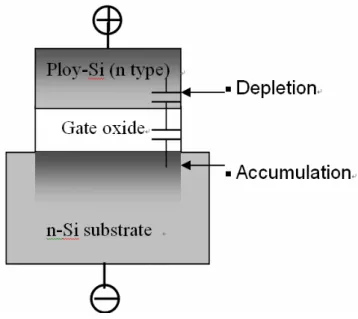
(6) 1. 前言 隨著積體電路技術朝向深次微米的極限發展,互補式金屬-氧化物-半導體場效電晶體 (complementary metal-oxide-semiconductor field effect transistor,簡稱 CMOS,為 pMOS 與 nMOS 相鄰並排的結構,如 Fig. 1-1 所示)的閘極氧化層(gate oxide)必須將厚度縮減,以增 加驅動電流(drive current, ID),維持載子的移動率,以及場效電晶體的跨導(transconductance) 和均勻的電場分佈,同時可以減少閘極延遲的時間(gate delay),對於電晶體的操作速度有 明顯的改善。 n+ Source/Drain. p+ Source/Drain. Gate Oxide Polysilicon. p-Si NMOS. SiO2. n-Si. Bulk Si. PMOS. SiO2. Fig. 1-1 CMOS 結構示意圖 [1] 閘極電極位於閘極氧化層之上,依其所加的電壓,將可造成矽基材的載子的累積 (accumulation)或空乏(depletion),因而使 MOSFET 產生導通或斷路的情況。因此閘極的作 用為操作 MOSFET 的關鍵,而 CMOS 可謂為整個積體電路運作的心臟。 在元件尺寸持續縮小的效應下,傳統的多晶矽(polycrystalline silicon, poly-Si)閘極電極 將面臨二個主要問題: (1) 在氧化層持續縮小下,p-MOSFET 中,作為電極的 p-type poly-Si 閘極,其中摻雜的硼 會在摻雜製程中或後續退火處理製程中穿透氧化層,稱為 boron penetration,而造成元 件起始電壓(Threshold voltage)的偏移[2,3],以及降低氧化層的可靠度。Fig. 1-2 為 PMOS 在摻雜硼的製程示意圖(source、drain、與 poly-Si gate 同時被摻雜)。由於硼為 一輕元素,因此容易由 poly-Si 進入氧化層或者穿透氧化層而進入下層的矽。. Poly-Si gate B. B. B oxide. n-Si substrate. Fig. 1-2 p-MOSFET 摻雜硼之製程及 boron penetration 示意圖 [4] (2) 在閘極施加電壓後,由於多晶矽亦具半導體特性,因此會如同矽基材一般產生空乏效 應,稱為 poly-depletion[5,6],因而降低了氧化層的電容值與通道中載子數目,影響了 MOSFET 的操作。如 Fig. 1-3 所示為 n-Si 基材與 n-type poly-Si 閘極,當閘極加上正電 1.
(7) 壓(基材相對而言為負偏壓)時,n-Si 基材會產生 carrier accumulation 而 n-type poly-Si 閘極會產生 depletion,因此在電極與氧化層之間增加了一個電容,而由於串聯電容數 目的增加而降低了整體電容值。. Fig. 1-3 多晶矽的空乏效應造成串聯電容 2001 國際半導體技術藍圖指出(International Technology Roadmap for Semiconductors, ITRS)[7],在 CMOS 結構中,閘極電極材料的選擇將有三大關鍵點:1功函數(work function),2低電阻率,3與 CMOS 技術的相容性。就元件設計的觀點而言,為了使起始 電壓達到適當之值,閘極電極材料的功函數為最重要的考量。應用於 pMOS 電晶體之閘極 電極,其費米能階(Fermi level,Evacuum-Efermi=qφ, φ=work function)必須接近矽基材的價 電帶(valence band)。而應用於 nMOS 電晶體之閘極電極,其費米能階則必須接近矽基材的 導電帶(conduction band)。由於 poly-Si gate 於製程中即摻雜與 source/drain 相同的摻雜物(n+ poly-Si for nMOS; p+ poly-Si for pMOS,稱為 auto-doping),因此自然可滿足上述之要求。然 而,若採用金屬作為閘極,pMOS 及 nMOS 可能必須為不同的金屬材料(稱為 dual-metal-gate),才能滿足閘極功函數的要求。Table 1-1 為 ITRS 認定具有潛力可作為閘極 電極材料之金屬或金屬化合物,而 Table 1-2 為常見閘極金屬以及矽的功函數值 [8-10]。 Gate electrode material NMOS. Ta, TaN, Zr, Hf, MSix, MNx, MSixNy. PMOS. Pt, Ru, RuO2, Ir, Ni, Co, WN, MSiy, MNy, MSixNy Table 1-1 ITRS 所列出之閘極電極材料[7]. Element. Φ (eV). Element. Φ (eV). Element. Φ (eV). Al (100). 4.2. Ir (100). 5.67. Si. 4.85. Co (polycr). 5.0. Ni (100). 5.22. Ta (polycr). 4.25. Cu (100). 5.10. Pt (polycr). 5.64. Ti (polycr). 4.33. Hf (polycr). 3.9. Ru (polycr). 4.71. W (polycr). 4.55. * polycr – Polycrystalline sample Table 1-2 元素功函數 [8-10] 倘若 pMOS 及 nMOS 必須採用不同的閘極金屬材料,可想而知製程的難度將明顯提高。 2.
(8) 折衷的方法之一為選取 Fermi level 約為 Si 的能隙中間值(mid-bandgap)的金屬,但這樣所 達到的起始電壓並不理想。最佳的情況仍舊是採用性質類似,但可調整功函數的材料, 同時作為 pMOS 及 nMOS 的閘極。由於金屬氮化物的功函數可藉由調整氮含量的成分而 加以調整,因此便成為閘極電極材料的新選擇。由於閘極結構屬於積體電路的前段製程, 因而完成閘極後,後續製程中仍有不少的加熱過程。因此,除了電阻率與功函數值之外, 閘極電極與氧化層之界面穩定性也是選擇閘極材料的一大考量。. 3.
(9) 2. 研究目的 在 CMOS 元件的製程中,傳統的多晶矽閘極電極面臨了一些問題,例如多晶矽的空乏 效應以及 P 型多晶矽發生硼穿透的現象發生,因而降低了電容器的整體電容值以及氧化 層的可靠度。因此,金屬或金屬氮化物成為取代多晶矽閘極電極材料的新選擇。以金屬 氮化物作為閘極電極,閘極中氮的含量以及結晶結構卻沒有詳細的研究資料。因此,本 研究第一階段將以不同氮含量的氮化鎢作為閘極電極,而以二氧化矽作為閘極氧化層, 研究氮含量對於氮化鎢作為閘極電極的影響。 由於金屬氮化物中氮的含量將會影響其作為閘極電極的表現,包括其熱穩定性及其 與氧化層之相容性的好壞,電阻值的高低,以及功函數值等。因此本研究以物理氣相沉 積法沉積氮化鎢薄膜,利用改變濺鍍氣氛的氮氣與氬氣的比率,得到三種不同成分比例 的氮化鎢薄膜。經由研究不同成分比例的氮化鎢薄膜對於熱穩定性,功函數值以及電容 器的電性結果之影響,可以得到以氮化鎢薄膜作為閘極電極材料時,其最佳之氮含量值。 在持續降低元件尺寸之際,若以二氧化矽作為閘極氧化層時,過薄的氧化層將會導 致穿遂電流的增加,因而導致元件的損壞。然而,若使用高介電常數材料作為閘極氧化 層,將可在不影響電荷儲存量之下而增加氧化層的厚度,因而降低氧化層之穿遂電流。 因此,本研究第二階段將以 Ta2O5 作為閘極氧化層材料,用以取代二氧化矽。在閘極電 極材料之選擇上,則以本研究第一階段所得最適宜之氮化鎢薄膜作為閘極電極材料,用 以取代傳統的多晶矽閘極電極。 由文獻比較得知,不同退火氣氛對於薄膜行為有相異的影響,造成此相異影響之來 源歸納有兩個:一為退火氣氛的差異對薄膜本身的影響,一為退火氣氛的差異對於薄膜 界面間的影響。因此後續退火氣氛之差異,將會對於電容器的電性行為以及與閘極電極 的界面狀態有不同的影響。經過不同氣氛的退火後,氮化鎢/五氧化二鉭/矽之電容器的熱 穩定性及電性表現為本研究第二階段之研究重點。. 4.
(10) 3. 文獻探討 3.1. 氮化鎢薄膜特性 目前的二元相圖工具書上不存在 W-N 相圖,而由許多研究顯示出氮化鎢薄膜主要有 W2N 與 WN 相,W2N 的結構有兩種,一為 cubic 結構,另一為 hexagonal 結構,一般鍍膜 形成之結構均為 cubic 結構。其晶格型態類似 NaCl 晶格,若 W 佔據 Na 位置,則 N 佔據” 半數”的 Cl 位置。WN 結構也有兩種,一為 cubic 結構,另一為 hexagonal 結構(WC type), 由於 WN 為一個不易形成的相,因此利用濺鍍方式不易形成此結構。W2N 化合物的密度為 18.0 g/cm3,WN 化合物的密度則為 16.0 g/cm3 [11]。 WNX 薄膜可用 RF sputtering [12-15]、reactive ion beam sputtering [16]和 CVD [17-21] 等方法製備。主要應用於砷化鎵之蕭特基(Schottky)接觸 [22],積體電路之擴散阻障層 [13, 14, 23],耐磨耗之硬覆膜,光學薄膜以及 MOS 電容器的電極 [24, 25]。現今許多研究除了 著重於 WNX 作為擴散阻障層的特性,另外也有研究其電阻率 [26],超導性質 [27],光學 性質 [28]和蕭特基阻障性質 [29, 30]等。 Fig.3-1 為大略的 W-N 之成分與退火條件所對應之成相圖 [31]。經由此圖可以明顯發 現,在氮氣流量不高時,薄膜會形成 amorphous 結構,而隨著氮氣流量的升高,薄膜會生 成 bcc-W2N 結構,氮原子主要填充於 W 原子所形成之八面體的格隙位置。由於 hexagonal-WN 為一個不穩定之相,所以薄膜通常不容易形成此相。將 WNX 薄膜退火後, 氮原子會由晶格中跑掉,因而最終形成 cubic-W。在一般薄膜濺鍍過程中,隨著氮流量的增 加,薄膜的結構逐漸由 α-W 轉為 α-W+amorphous WNX,再轉為 W2N,在 600oC 退火下, W2N 會轉變為 α-W+amorphous WNX [32]。 WNX 薄膜的電阻率隨著氮含量增加而增加,若薄膜中含有微量氮成份,而薄膜為 W 結構,則其電阻率大約介於 100 ~ 200μΩ-㎝之間,若薄膜有 WNX 相形成,隨著 X 範圍的加 大,電阻率會由 300μΩ-㎝增加至 2000μΩ-㎝以上 [15, 33]。 WNX 薄膜的氮成份隨著濺鍍功率的增加而降低,濺鍍時工作壓力的升高而升高,以及 氮流量的增加而升高 [34]。若 WNX 薄膜中含有 35 ~ 55%的氮(利用 XPS 計算而得),則 晶格常數為 4.15 ~ 4.20Å 之間,此時薄膜的結構為 W2N,由於氮原子的填入會使得晶格產 生膨脹現象,因此 W2N 薄膜的晶格常數通常會大於塊材的晶格常數 4.126Å [35],而高溫退 火後會降低其晶格常數 [36]。. Fig.3-1 W-N 成分與退火溫度所對應之成相圖 [31]. 5.
(11) 3.2 五氧化二鉭薄膜特性 Ta2O5 為一高介電常數材料,近年來廣泛的被研究於取代傳統的二氧化矽閘極氧化 層之可行性。其製備方法以 PVD 與 CVD 兩種製程為主,初鍍的 Ta2O5 為非晶結構,在 氧氣退火至 600oC 仍為非晶結構,其介電常數約為 25~30;若退火溫度達到 800oC,則非 晶結構會轉為 orthorhombic 結構或 hexagonal 結構(β-Ta2O5 或 δ-Ta2O5) ,其介電常數約 為 40~60 [37-39]。在非晶結構中,隨著氧氣退火溫度的升高,Ta2O5 中的缺陷與應力會 消除,因此使得漏電流降低;但在結晶結構中,隨著氧氣退火溫度的升高,則 Ta2O5 的 晶界會使得漏電流增加 [38],而結晶結構的 Ta2O5 則會有較少的氧化層固定電荷 [38]。 另外,以 425 oC 之 N2 或 N2+H2 混合氣體退火 Al/Ta2O5 後,則會發現 Ta2O5 的漏電流在 退火後則呈現降低的趨勢,且以混合氣體退火之試片其降低幅度較大 [40]。. 6.
(12) 4. 研究方法 本研究第一階段使用金氧半電容器為結構,其中以 N 型 (100) 矽(1~10Ω-㎝)為基材, 以高溫爐管熱氧化方式置備二氧化矽薄膜作為閘極氧化層,再以物理氣相沉積法製備氮化 鎢薄膜作為閘極電極。高溫爐管反應溫度為 1050℃,利用橢圓儀量測所得二氧化矽薄膜厚 度約為 25nm。完成之二氧化矽薄膜上方以物理氣相沉積法沉積氮化鎢薄膜,利用改變濺鍍 氣氛的氮氣與氬氣的比率,得到三種不同成分比例的氮化鎢薄膜,薄膜的厚度均約為 170nm。製作完成金氧半電容器後,後續退火處理採用爐管退火,其退火氣氛為混合氣體 (10%氫氣與 90%氮氣),退火時間為 30 分鐘,退火溫度分別為 400、500oC。 經由拉塞福背向散射成分分析去計算氮化鎢薄膜中氮與鎢的成分比,利用低掠角 X 光 繞射儀的繞射分析得到薄膜的結晶結構,並利用 X 光光電子能譜分析薄膜的化學鍵結。經 由歐傑電子能譜儀分析元素縱深成份分佈,我們可得到經過退火後氧原子於氮化鎢薄膜中 之分佈。利用穿透式電子顯微鏡分析,我們可以觀察閘極與氧化層的界面現象。使用四點 探針量測氮化鎢之 V/I 值,且計算閘極之片電阻值。並以 HP4140B 量測不同成分組成的氮 化鎢閘極對於整體電容器結構的漏電流影響。以及 HP4284 量測不同試片的 C-V 曲線,經 由 C-V 曲線可得知不同的氮化鎢閘極在經過退火後對於平帶偏壓(VFB)偏移的影響。量測 C-V 遲滯曲線主要目的為得到慢速捕獲電荷(slow trapped charge)的密度,探討不同氮化鎢 閘極是否會對慢速捕獲電荷有影響。 第二階段則以有機金屬氣相沉積法(MOCVD)製備 Ta2O5 薄膜於矽基材上以作為閘極氧 化層,後再以物理氣相沉積法(PVD)製備 WNx 薄膜作為閘極電極。MOCVD 系統採用 [Ta(OC2H5)5]作為前驅物,氧氣為反應氣體,反應溫度為 450oC,薄膜的厚度控制在 15nm 左右,以橢圓儀精確量測 Ta2O5 薄膜的厚度。在完成 Ta2O5 薄膜沉積後,利用氧氣退火 Ta2O5 薄膜,退火溫度為 800oC,退火時間為 30min,退火後之 Ta2O5 薄膜為結晶性。完成之 Ta2O5 薄膜上方再以 PVD 系統沉積 WNx 薄膜,厚度約為 200nm。在製作完成 MOS 電容器後,後 續退火處理採用爐管退火,其分為兩種:1 H2 退火 30min,210%H2+N2 退火 30min,退 火溫度分別為 400、500 及 600oC。 經由 AES 縱深分析,我們將可以得到氮原子於 WNx 薄膜中之逸散行為,因此可以 比較退火氣氛的差異對於 WNx 薄膜的影響。以 HP4140B 量測不同退火製程的漏電流變 化,我們將可以利用漏電流的變化選擇出較理想的退火處理。以 HP4284 量測不同試片 的 C-V curve,經由 C-V curve 可以得知不同的退火處理對於 VFB 偏移的影響,且經由 VFB 偏移量可以比較氧化層中 Qf (Fixed charge)的增減。量測 C-V hysteresis curve 主要目的為 得到 slow trapped site 的密度,探討不同退火氣氛是否會對 slow trapped site 有影響。. 7.
(13) 5. 結果與討論 5.1. 氮化鎢閘極成分分析與功函數 經由改變濺鍍的氮氣與氬氣的比率,我們可以得到三種不同成分比例的氮化鎢薄膜, 並利用拉塞福背向散射成分分析,計算而得氮化鎢薄膜的氮:鎢分別為 1:0.6,1:0.8 以 及 1:1.5,因此我們分別以 WN0.6、WN0.8、WN1.5 稱呼此三種氮化鎢薄膜。 本研究是採用 C-V curve 方法直接量取金屬與半導體的功函數差(Φms)。由公式(1)可得 [41]:. VFB = Φ ms −. Q. kε o A. t. ------ (1). 其中 Q 為氧化層中電荷數,t 為氧化層厚度。利用不同氧化層厚度對平帶電壓作圖,即可 由截距得到 Φms 之值。再利用所得到的 Φms 加上矽的功函數 Φs,則可以得到金屬氮化物的 功函數 Φm。Fig.5-1(a) (b) (c)為以 WN0.6、WN0.8、WN1.5 的電容器其不同氧化層厚度對平帶 電壓作圖結果。Table 5-1 列出利用電容器的平帶電壓(VFB)對氧化層的厚度作線性分析而得 到 Φms,亦列出經由計算所得到氮化鎢閘極的功函數值。在本研究中,矽的功函數 Φs 值為 4.31 eV。由功函數值可知,WN0.8 閘極的功函數為最高,其值為 5.01 eV,而 WN0.6 和 WN1.5 的功函數值則略微接近,其值分別為 4.50 eV 和 4.49 eV。 1. (a) WN0.6. 2 (b) WN0.8 0. Flat band voltage (V). Flat band voltage (V). 0 -1 -2 -3 -4 -5. -2 -4 -6 -8 -10 -12. 0. 10. 20. 30. 40. 50. 60. 0. SiO2 thickness (nm) 2. 20. 40. 60. 80. 100. SiO2 thickness (nm). (c) WN1.5. Flat band voltage (V). 0 -2 -4 -6 -8 -10. 0. 20. 40. 60. 80. 100. SiO2 thickness (nm). Fig.5-1 不同氧化層厚度對以氮化鎢為閘極之電容器平帶電壓之作圖結果(a)WN0.6(b)WN0.8 (c)WN1.5. 8.
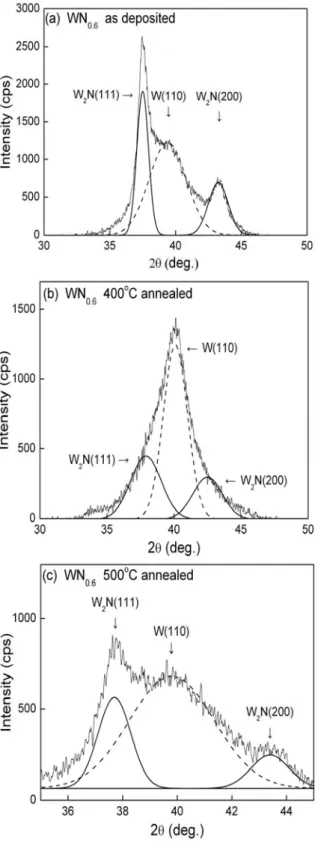
(14) WNx. Φms (eV). Φm (eV). WN0.6. 0.20. 4.40. WN0.8. 0.71. 4.91. WN1.5. 0.18. 4.38. Table 5-1 不同氮含量的氮化鎢閘極電極,電容器的平帶電壓(Φms)與氮化鎢的功函數值(Φm) 5.2. 氮化鎢閘極繞射結構 在退火前後 WN0.6、WN0.8、WN1.5 薄膜的結晶結構變化則利用低掠角 X 光繞射儀的繞 射分析之。Fig.5-2 顯示在不同的退火溫度下,氮化鎢薄膜繞射結構變化。由 Fig. 5-2 (a)可 以發現在未退火的 WN0.6 薄膜含有結晶態的 W 與 W2N,由於在 2θ 約為 40o 處之繞射峰有 明顯的重疊,因此 Fig. 5-3 (a)(b)(c)為 WN0.6 薄膜在未退火及退火 400oC 及 500oC 的繞射峰 分解結果。由此結果可以得知,在經過退火後,WN0.6 薄膜仍然為 W 與 W2N 的混合相。且 經過 500oC 的退火後,WN0.6 薄膜出現明顯的 WO3 相,顯示薄膜明顯被氧化。而從 Fig. 5-2 (b)和 Fig. 5-2 (c)的結果可知,WN0.8 與 WN1.5 薄膜均顯示結晶態的 W2N 結構,且在經過 500oC 的退火後,薄膜仍是呈現單一的 W2N 結構。此結果顯示增加氮化鎢閘極中的氮含量可以提 高氮化鎢閘極的熱穩定性。. Fig.5-2 不同退火溫度下的氮化鎢閘極之低掠角 X 光繞射儀分析結果(a)WN0.6(b)WN0.8 (c)WN1.5. 9.
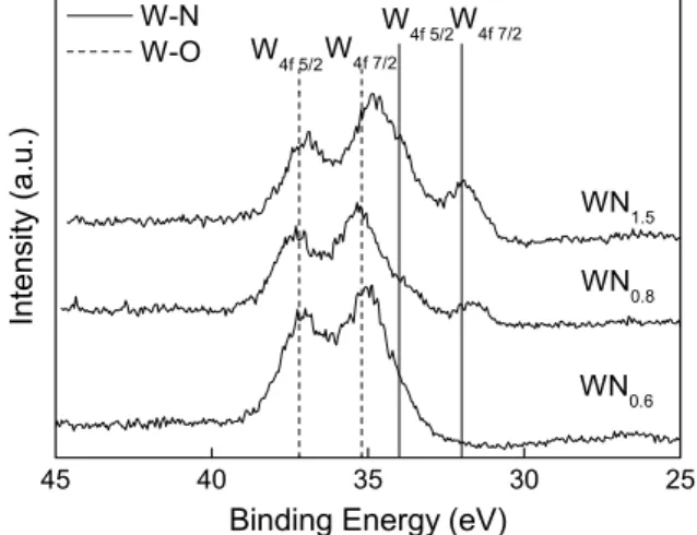
(15) Fig.5-3 WN0.6 薄膜之低掠角 X 光繞射峰分解結果(a)未退火(b)400oC 退火(c) 500oC 退火 5.3. 氮化鎢閘極化學鍵結分析 在經過 500oC 的退火後,WN0.6、WN0.8、WN1.5 薄膜的化學鍵結分析結果顯示於 Fig.5-4。 W4f 圖譜含有兩組 doublets,低能量的兩根 doublets 為 W-N 鍵結,而高能量的兩根 doublets 則為 W-O 鍵結。由圖譜可以明顯得知,經過 500oC 的退火後的 WN0.6 薄膜僅存有 W-O 鍵 結,而 WN0.8、WN1.5 薄膜則同時具有 W-N 鍵結與 W-O 鍵結,且 W-N 鍵結的能量亦隨著 氮化鎢薄膜中氮含量的增加而增加。此化學鍵結分析結果亦與低掠角 X 光繞射分析結果相 符合,顯示高溫退火後 WN0.6 薄膜明顯被氧化。. Fig.5-4 WN0.6、WN0.8 與 WN1.5 在 500oC 退火後 X 光光電子能譜分析. 10.
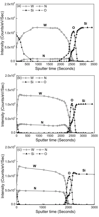
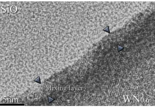
(16) 5.4. 氮化鎢閘極之歐傑電子能譜儀縱深分析 為了得知在經過 500oC 的退火後氮化鎢閘極內部的元素分佈情形,於是我們利用歐傑 電子能譜儀縱深分析觀察氮化鎢/二氧化矽/矽試片的元素分佈狀況。Fig.5-5(a)(b)(c)顯示在 退火後 WN0.6、WN0.8、WN1.5 閘極的分析結果。由 Fig.5-5(a)可以明顯得知,WN0.6 閘極被 氧化的主要原因是來自於外界的氧氣提供了氧化發生的主要來源。然而在 WN0.6 閘極與二 氧化矽界面處亦發現有一層明顯的混合層產生,顯示二氧化矽中的氧亦擴散進入 WN0.6 薄 膜,導致氮化鎢與二氧化矽界面產生反應。相較於 WN0.6 閘極,由 Fig.5-5(b)以及 Fig.5-5(c) 可知,WN0.8 與 WN1.5 閘極在經過退火後,其表面雖然有氧化現象產生,但是氧化程度並不 如 WN0.6 閘極來的嚴重,且在與二氧化矽接觸的界面處亦沒有明顯的混合層產生,顯示提 高氮化鎢中的氮含量能夠有效抑制氮化鎢薄膜被氧化的情形,亦即提高氮化鎢的熱穩定性。. Fig.5-5 氮化鎢/二氧化矽/矽結構在 500℃退火後的歐傑電子能譜儀縱深分析(a)WN0.6 (b)WN0.8(c)WN1.5 5.5. 氮化鎢(WN0.6)/二氧化矽界面分析 由於從歐傑電子能譜儀縱深分析得知 WN0.6 閘極與二氧化矽界面處有一層混合層產 生,於是我們利用穿透式電子顯微鏡分析觀察此混合層之型態。Fig.5-6 為氮化鎢(WN0.6)/ 二氧化矽/矽橫截面圖。由分析結果可以得知此混合層並沒有明顯的分界線,亦即此混合層 並不具有平整性。此混合層的產生對於整體電容器的電性行為是否有影響,則為研究之重 點。. 11.
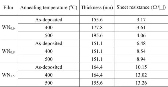
(17) Fig.5-6 氮化鎢(WN0.6)/二氧化矽/矽結構的橫截面型態 5.6. 氮化鎢厚度及片電阻量測 Table 5-2 列出不同氮含量之氮化鎢的厚度以及片電阻值。在高溫退火後,由於閘極氧 化的發生,使得 WN0.6 閘極的厚度與片電阻值明顯增加。Fig.5-7(a)(b)顯示 WN0.6 閘極在未 退火及退火 500oC 後其薄膜利用 SEM 分析所得之橫截面結果。由結果可以明顯得知在退火 後 WN0.6 閘極的表面有明顯的變化,且根據 AES 分析結果可得,造成此變化的主因應是 WN0.6 閘極的表面被氧化之關係。由片電阻值可知,閘極氮含量的增加亦明顯的增加其片電 阻值。此結果顯示低氮含量之氮化鎢閘極有較好的導電性。. Film. WN0.6. WN0.8. WN1.5. Annealing temperature (oC). Thickness (nm). Sheet resistance (Ω/□). As-deposited. 155.6. 3.17. 400. 177.8. 3.61. 500. 195.6. 4.06. As-deposited. 151.1. 6.48. 400. 151.1. 8.54. 500. 151.1. 8.94. As-deposited. 164.4. 10.15. 400. 164.4. 13.02. 500. 155.6. 13.26. Table 5-2 氮化鎢薄膜在不同退火溫度的厚度及片電阻值. 12.
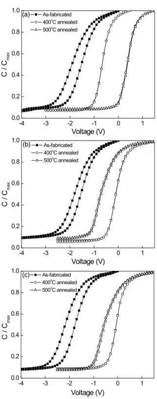
(18) (a). (b). WN0.6. WN0.6. Fig.5-7 WN0.6 薄膜 SEM 分析之橫截面結果(a)未退火(b) 500oC 退火 5.7. 氮化鎢/二氧化矽/矽之 C-V 遲滯曲線 Fig.5-8(a)(b)(c)顯示在不同的退火溫度下,氮化鎢/二氧化矽/矽電容器結構之 C-V 遲 滯曲線。經由 C-V 遲滯曲線計算出氧化層內部慢速捕獲電荷的量 Nh,亦列於 Table 5-3。 Nh 值之計算可由公式(2)所得[42]。. Nh =. Cox ΔV fb ,hysteresis. ------ (2) . qA. 其中 Cox 為氧化層電容值,ΔVfb,hysteresis 為 C-V 曲線由空乏層掃描到聚積層再掃描回空乏層後 其兩條曲線之偏移量,而 q 為電荷量,A 則為電極面積。由結果可以得知不同成分比例的 氮化鎢閘極對於 Nh 值並不會有明顯的影響,而在經過 400oC 退火後,由於退火氣氛對於氧 化層缺陷的修補作用因而降低了 Nh 值。但在經過 500oC 退火後,由於氧化層內部缺陷反而 會上升,因此提高了 Nh 值[43]。Table 5-3 亦列出在經過退火後電容器的 C-V 曲線相較於未 退火電容器的 C-V 曲線偏移量。由此偏移量可以看出,WN0.8 與 WN1.5 閘極的電容器結構 其 C-V 曲線在經過 400oC 退火後會往正偏壓的方向偏移(相較於未退火的電容器結構的 C-V 曲線),其主要原因是因為 Nh 值在 400oC 退火後降低的關係,然而經過 500oC 退火後,由 於 Nh 值的升高,因而使得 WN0.8 與 WN1.5 閘極的電容器結構其 C-V 曲線往負偏壓的方向偏 移(相較於 400oC 退火的電容器結構的 C-V 曲線)。對於 WN0.6 閘極的電容器結構其 C-V 曲 線在經過 400oC 退火後仍然會往正偏壓的方向偏移(相較於未退火的電容器結構的 C-V 曲 線),其主要原因也是因為 Nh 值在 400oC 退火後降低的關係,但是與 WN0.8 與 WN1.5 閘極 的電容器不同的是,在經過 500oC 退火後,其 C-V 曲線明顯往正偏壓的方向偏移(相較於 400oC 退火的電容器結構的 C-V 曲線)。由於經過 500oC 退火後的歐傑電子能譜儀縱深分析 可知,在 WN0.6 閘極與二氧化矽界面處亦發現有一層明顯的混合層產生,顯示二氧化矽中 的氧亦擴散進入 WN0.6 薄膜,因此導致二氧化矽薄膜內部的缺陷增多,因而導致 C-V 曲線 往正偏壓的方向偏移。. 13.
(19) Fig.5-8 不同退火溫度氮化鎢/二氧化矽/矽結構之高頻 C-V 曲線變化(a)WN0.6 (b)WN0.8 (c)WN1.5. 薄膜. WN0.6. 退火溫度(oC). Nh(cm-2). △VFB (V). As- fabricated. 3.34×10¹¹. ---. 400. 3.81×10. 9. 1.25. 500. 2.02×10¹⁰. 2.30. As- fabricated WN0.8. ---. 9. 1.70. 10. 1.21. 11. ---. 2.99×10. 400. 9.71×10. 500. 3.47×10. As- fabricated WN1.5. 11. 3.81×10. 400. 2.63×10⁹. 2.25. 500. 10. 1.64. 5.07×10. Table 5-3 不同退火氣氛下,氮化鎢/二氧化矽/矽電容器的氧化層之捕獲電荷量(Nh),以及 C-V 曲線的偏移量 (△VFB=(退火後電容器的平帶偏壓)-(未退火電容器的平帶偏壓)) 5.8. 氮化鎢/二氧化矽/矽之漏電現象 Table 5-4 列出當施加+1 與-1MV/cm 電場於閘極上方時,電容器的電流密度大小。由 此結果可以明顯得知,不管氮化鎢閘極的成分比為何,均不會影響整體電容器的漏電流 大小,然而當閘極上方施加負偏壓時其漏電流會明顯大於在閘極上方施加正偏壓時的漏 14.
(20) 電流,其原因為在濺鍍氮化鎢薄膜時,會造成二氧化矽與氮化鎢的界面處有氧空缺的產 生,因而造成漏電流增加[44]。 電流密度 (A/cm2). o. 退火溫度( C). 薄膜. +1 MV/cm. -1 MV/cm. As- fabricated. 3×10⁻¹⁰. 2×10⁻⁸. 400. 3×10⁻¹⁰. 4×10⁻⁸. 500. 1×10⁻⁹. 5×10⁻⁸. As- fabricated. 5×10⁻¹⁰. 3×10⁻⁸. 400. 6×10⁻¹⁰. 4×10⁻⁸. 500. 1×10⁻⁹. 2×10⁻⁸. As- fabricated. 6×10⁻¹⁰. 3×10⁻⁸. 400. 1×10⁻⁹. 6×10⁻⁸. 500. 9×10⁻¹⁰. 6×10⁻⁸. WN0.6. WN0.8. WN1.5. Table 5-4 不同退火氣氛下,氮化鎢/二氧化矽/矽電容器的漏電流值 5.9 WN0.8 閘極繞射結構 本研究之第二階段選用 WN0.8 作為閘極電極,研究其與高介電係數材料 Ta2O5 之熱穩定 性及 WN0.8/Ta2O5/Si 電容器之電性表現。Fig.5-9 顯示在不同的退火溫度和退火氣氛下,WN0.8 薄膜繞射結構的改變。當退火溫度為 400-500 oC 時,WN0.8 薄膜為 W2N 相,在退火溫度升 高到 600 oC 後,WN0.8 薄膜出現 WO3 相。由 GIAXRD 的繞射分析結果可知,當退火溫度達 600 oC 時,不論在何種退火氣氛中,WN0.8 薄膜的表面均會被氧化,而形成 WO3 與 W2N 的 混合結構。 ★W2N ☆WO3. ★ ☆. ☆. ★. ☆★ ☆ ☆ ☆. ★ g. Intensity (a.u.). ☆. f e d c b a. 20. 30. 40. 50. 60. 70. 80. 2θ (deg.). Fig.5-9 不同退火氣氛與溫度下的 WN0.8 閘極之 GIAXRD 繞射分析結果(a)未退火(b)400 oC H2 退火(c)400 oC H2+N2 退火(d)500 oC H2 退火(e)500 oC H2+N2 退火(f)600 oC H2 退 火(g) 600 oC H2+N2 退火. 5.10 WN0.8 閘極之 AES 縱深分析 Fig.5-10 (a)(b)顯示在 H2 或 H2+N2 退火氣氛下退火 600 oC 後,WN0.8/Ta2O5/Si 試片的 15.
(21) Intensity (Counts/eV/Sec). AES 縱深分析結果。由 Fig.5-10 (a)可明顯發現,在 600 oC H2 退火下,WN0.8 閘極中的氮原 子明顯的減少,且 WN0.8 內部有著多量的氧原子。而在 600 oC 混合氣體退火下(Fig.5-10 (b)),雖然 WN0.8 表面有氧化的現象發生,但是 WN0.8 內部的氮原子並沒有明顯減少的情況 產生。由於在高溫退火後,WN0.8 薄膜內部的氮原子有向薄膜表面逸散的情形發生[12,31], 因而降低了薄膜內部的氮含量。經由比較不同退火氣氛下,氮原子的在薄膜中的含量,我 們可以清楚發現 H2+N2 的退火氣氛能有效的阻止 WN0.8 內部的氮原子往外界逸散的現象發 生,因而能夠維持 WN0.8 薄膜的穩定性。 4.0x10. 6. 3.5x10. 6. 3.0x10. 6. 2.5x10. 6. 2.0x10. 6. 1.5x10. 6. 1.0x10. 6. 5.0x10. 5. N Ta. (b). 0.0. W O. Si. W. N O 0. 1000. 2000. 3000. 4000. 5000. Sputter time (Seconds). Fig.5-10 WN0.8/Ta2O5/Si 結構在 600 oC 退火後的 AES 縱深分析(a) H2 退火氣氛(b) H2+N2 退 火氣氛 5.11 WN0.8 閘極電阻率 Fig.5-11 顯示在不同的退火溫度和退火氣氛下,WN0.8 薄膜電阻率的變化情形。在退火 溫度達 500 oC 時,薄膜的電阻率有約略上升的現象。當退火溫度達 600 oC,薄膜的電阻率 明顯的升高,而且在 H2 退火後的 WN0.8 薄膜,其電阻率升高的幅度最大。WN0.8 薄膜電阻 率的上升主要是因為在高溫退火後,WN0.8 的表面有被氧化的現象發生,因而提高了電阻 率。且由 AES 縱深分析可知,在 600 oC 的 H2 退火氣氛下之 WN0.8 薄膜表面有較嚴重的氧 化現象產生,因此其電阻率上升之幅度非常大。 1700. H2 annealing N2+H2 annealing. Resistivity (μ Ω -cm). 1600 1500 800 700 600 0 100 as-dep.. 200. 300. 400. 500. 600. o. Annealing Temperature ( C). Fig.5-11 不同退火溫度與退火氣氛下的 WN0.8 薄膜之電阻率變化 5.12 WN0.8/Ta2O5/Si 之 C-V 曲線 Fig.5-12 顯示在不同的退火溫度和退火氣氛下,WN0.8/Ta2O5/Si 之高頻(100k) C-V 曲線 16.
(22) 的變化。Table 5-5 列出在退火過後,WN0.8/Ta2O5/Si 之 C-V 曲線偏移量ΔVFB (與未退火的 結構相比較下)及 Ta2O5 氧化層的介電常數 k, k 值之測量是利用當施加電壓為 2V 時,量 測到電容值 C,利用公式(3),即可得到氧化層的介電常數 k。 kε o A ------ (3) d 其中 ε o 為真空介電率,A 為電極面積,d 為 Ta2O5 薄膜的厚度。 C=. ΔVFB 的量與氧化層的缺陷有關,由公式(4)可知[45] ΔQ ΔVFB = Φ ms − C ox. ------ (4). 其中Φms 為金屬閘極與半導體層的功函數差,ΔQ 為氧化層的電荷,Cox 為氧化層的電容值。 在高溫退火後,雖然 WN0.8 閘極的表面有氧化的現象產生,但是在 WN0.8 閘極與 Ta2O5 氧化. Capacitance (F). 層的界面並沒有明顯的反應發生,因此 WN0.8/Ta2O5/Si 之 C-V 曲線偏移量ΔVFB(≦0.1V)與 氧化層的介電常數 k,在經過高溫退火後並沒有明顯的變化發生。由此結果可以發現在 600 o C 退火後,WN0.8 閘極與 Ta2O5 氧化層的界面仍然可以維持在很穩定的狀態。 1.4x10. -10. 1.2x10. -10. 1.0x10. -10. 8.0x10. -11. 6.0x10. -11. 4.0x10. -11. 2.0x10. -11. As-fabricated o H2 400 C o. H2 500 C o. H2 600 C. o. N2+H2 400 C o. N2+H2 500 C o. N2+H2 600 C. 0.0 -2. -1. 0. 1. 2. Voltage (V). Fig.5-12 不同退火溫度與退火氣氛下的 WN0.8/Ta2O5/Si 結構之高頻 C-V 曲線變化 退火氣氛/溫度. ΔVFB(V). k. Nh(cm-2). 未退火. -. 12.3. +4.94×10¹². H2 / 400oC. 0.1. 11.6. +1.13×10¹². H2 / 500oC. 0.05. 12.3. +7.22×10¹¹. H2 / 600oC. 0.07. 12.3. -7.14×10¹¹. N2+H2 / 400oC. 0.08. 13.2. -8.47×10¹¹. N2+H2 / 500oC. 0.06. 12.2. -5.50×10¹¹. N2+H2 / 600oC. 0.06. 11.1. -6.95×10¹¹. Table 5-5 不同退火氣氛與溫度下的 C-V 曲線偏移量(ΔVFB)、氧化層介電常數值(k)與氧化 層之捕獲電荷量(Nh) 5.13 WN0.8/Ta2O5/Si 之遲滯 C-V 曲線 Fig.5-13 顯示在不同的退火溫度和退火氣氛下,WN0.8/Ta2O5/Si 之遲滯 C-V 曲線。經由 遲滯 C-V 曲線計算出氧化層內部 slow trapped site 的量 Nh,亦列於 Table 5-5。Nh 值之計算 亦由公式(2)所得。 17.
(23) 在 Ta2O5 氧化層經過 800oC 高溫退火後,Si 與 Ta2O5 界面一定會生成一層 SiO2[40],這 層 SiO2 與 Si 界面會有一些正的捕獲電荷產生[46],而 Ta2O5 內部則會有負的電子電荷存在 [47,48],此兩種電荷造成了遲滯 C-V 曲線的變化情形。經由計算氧化層內部 slow trapped site 的量 Nh 可以得知,在經過 400oC H2+N2 的退火後,可以明顯的降低 SiO2 與 Si 界面正捕獲 電荷的數量,因而經由計算所得的 Nh 為負值,且其數量在 1011cm-2 左右;而在 600oC 的 H2 退火後,才能顯著的降低 SiO2 與 Si 界面正捕獲電荷的數量,使得 Nh 數量在 1011cm-2 附 近。. 1.4x10. -10. 1.2x10. -10. 1.0x10. -10. 8.0x10. -11. 6.0x10. -11. -11. 4.0x10. -11. -11. 2.0x10. -11. -10. 1.4x10. (a). As-fabricated o H2 400 C. -10. 1.2x10. o. Capacitance (F). Capacitance (F). H2 500 C. -10. 1.0x10. o. H2 600 C. -11. 8.0x10. -11. 6.0x10 4.0x10 2.0x10. 0.0. -3. (b). o. N2+H2 500 C. 0.0. -2. -1. 0. 1. 2. -3. 3. As-fabricated o N2+H2 400 C o. N2+H2 600 C. -2. -1. 0. 1. 2. 3. Voltage (V). Voltage (V). Fig.5-13 不同退火溫度與退火氣氛下的 WN0.8/Ta2O5/Si 結構之高頻 C-V 曲線變化(a) H2 退火 氣氛(b) H2+N2 退火氣氛 5.14 WN0.8/Ta2O5/Si 之 I-V 曲線 Fig.5-14 (a)(b)分別顯示在不同的退火溫度和退火氣氛下,WN0.8/Ta2O5/Si 結構在施加正 偏壓與負偏壓的 I-V 曲線變化情形。由 Fig.5-14 (a)可得,當閘極上方施加正偏壓時,顯示 電子流由 Si 基材進入 Ta2O5 氧化層,由於 Si 與 Ta2O5 界面會生成一層 SiO2,因此漏電流的 大小將由 SiO2 所主導。在退火 400oC 後,SiO2 與 Si 界面的缺陷有增加的現象,因而漏電流 有約略上升的現象,當退火溫度持續升高,由於氫原子有填補 SiO2 與 Si 界面斷鍵的功用, 因而降低了界面缺陷,亦降低了整體的漏電流值。另外,H2 退火氣氛比 H2+N2 退火氣氛 有較佳的填補界面斷鍵效能,因此當閘極上方施加正偏壓時,採用 H2 退火氣氛的試片結構 有較低的漏電流值。 當閘極上方施加負偏壓時,顯示電子流由 WN0.8 閘極流往 Ta2O5 氧化層,由於在退火過 後,WN0.8 與 Ta2O5 界面仍維持很穩定的狀態,所以漏電流並沒有明顯的變化情形發生。此 外,因為當閘極上方施加負偏壓時,Si 基材此時會產生空乏層,此層空乏層的產生應是造 成在閘極上方施加負偏壓時的漏電流小於在閘極上方施加正偏壓時漏電流的主要原因。. 18.
(24) -4. 10 (a). -4. 10 (b). As-fabricated o H2 400 C. As-fabricated o H2 400 C. o. 10. -5. H2 500 C o. H2 600 C. 10. -5. 10. -6. o. H2 500 C o. H2 600 C. 10. o. N2+H2 500 C o. N2+H2 600 C. 10. -7. 10. -8. 0.0. 0.5. 1.0. o. N2+H2 400 C. 2. -6. J (A/cm ). 2. J (A/cm ). o. N2+H2 400 C. 1.5. 2.0. 2.5. E (MV/cm). o. N2+H2 500 C o. N2+H2 600 C. 10. -7. 10. -8. -2.5. -2.0. -1.5. -1.0. -0.5. 0.0. E (MV/cm). Fig.5-14 不同退火溫度與退火氣氛下的 WN0.8/Ta2O5/Si 結構之 I-V 曲線變化(a)閘極上方施加 正偏壓(b)閘極上方施加負偏壓. 19.
(25) 6. 結論 本研究第一階段主要討論不同成分比的氮化鎢閘極對於功函數值、熱穩定性和電性 的影響。改變氮化鎢薄膜的氮含量,除了會改變其功函數外,且經過 400 和 500oC 退火 後,會對於氮化鎢閘極的結晶結構、化學鍵結、片電阻值、以及元素分佈情形有所影響, 然而在電容器的漏電行為上則不會因為氮化鎢閘極的氮含量多寡而影響其結果。對低氮 含量的 WN0.6 閘極而言,由於在退火後容易被氧化,因而導致閘極表面及與二氧化矽接 觸的界面間皆有明顯的氧原子訊號。因此,在選用氮化鎢為閘極材料時,仍以高氮含量 的 WN0.8 與 WN1.5 閘極為較佳的選擇。但由於閘極電極需要低電阻率之考量,因此在選 用閘極電極的材料上,仍以 WN0.8 為最佳之氮化鎢閘極電極。 而在第二階段的研究中,在 WN0.8/Ta2O5/Si 的電容器結構中,當退火溫度達 500oC 時, WN0.8 閘極仍然維持於一個很穩定的狀態,而在退火溫度達 600oC 後,WN0.8 閘極表面有氧 化的現象發生,且提高了其電阻率。在 H2 退火氣氛中,氮原子由 WN0.8 閘極逸散出去的現 象較為明顯,而 H2+N2 的退火氣氛則能有效的阻擋氮原子的逸散現象且維持 WN0.8 閘極的 熱穩定性。在經過高溫退火後,WN0.8 閘極與 Ta2O5 氧化層界面仍維持在很穩定的狀況下, 因此 Ta2O5 氧化層的介電常數與缺陷並不隨著高溫退火而改變。在 H2 退火氣氛中,由於具 有比較優良填補基材與氧化層界面斷鍵缺陷的能力,因此可以較明顯的降低漏電流的現象 發生。而 H2+N2 的退火氣氛則可以明顯的改善氧化層中捕獲電荷的數目。. 20.
(26) 7. 參考文獻 1. Modified from H. Xiao, “Introduction to Semiconductor Manufacturing Technology”, Prentice Hall, New Jersey, USA, 2000. 2. K. S. Krisch, M. L. Green, F. H. Baumann, D. Brasen, L. C. Feldman, L. Manchanda, IEEE Trans. on Electron Devices 43, 982 (1996). 3. Z. J. Ma, J. C. Chen, Z. H. Liu, J. T. Krick, Y. C. Cheng, C. Hu, P. K. Ko, IEEE Electron Device Lett. 15, 109 (1994). 4. Modified from Plummer, Deal and Griffin, “Silicon VLSI Technology”, Chap. 2, (Prentice Hall, New Jersey, USA, 2000). 5. C. Leveugle, P. K. Hurley, A. Mathewson, S. Moran, E. Sheehan, A. Kalnitsky, A. Lepert, I. Beinglass, M. Venkatesan, Microelectronic Engineering 36, 215 (1997). 6. W. –J. Cho, J. –E. Hong, W. –H. Jin, K. –S. Lee, S. –K. Rha, H. –S. Kim, Solid-State Electronics 44, 393 (2000). 7. International Technology Roadmap for Semiconductors, 2001 editon, Semiconductor Industry Association. 8. J. Hölzl and F. K. Schulte, Work Functions of Metals, in Solid Surface Physics, edited by G. Höhler, Springer-Verlag, Berlin (1979). 9. J. C. Riviere, Work Function: Measurements and Results, in Solid State Surface Science, Vol. 1, edited by M. Green, Decker, New York (1969). 10. H. B. Michaelson, J. Appl. Phys. 48, 4729 (1977). 11. M. Hansen, “Constitution of binary alloys”, 2nd edition, McGraw Hill Book Company, New York, 1958. 12. K. Affolter, H. P. Kattelus, M.-A. Nicolet, MRS Sym. Proc. Vol. 47, Materials Research Society, Pittsburgh, 47, 167(1985). 13. H. P. Kattelus, E. Kolawa, K. Affolter, M.-A. Nicolet, J. Vac. Sci. Technol. A 3 ,2246(1985). 14. F.C.T. So, E. Kolawa, X.-A. Zhao, M.-A. Nicolet, J. Appl. Phys. 64, 2787(1988). 15. K. J. Huber, C. R. Aita, J. Vac. Sci. Technol. A 6, 1717(1988). 16. H. L. Zhang, D. Z. Wang, N. K. Huang, Appl. Surf. Sci. 150, 34(1999). 17. T. Nakajima, K. Watanabe, N. Watanabe, J. Electrochem. Soc. 134, 3175(1987). 18. Y. T. Kim, C. W. Lee, S.-K. Min, Appl. Phys. Lett. 61, 537(1992). 19. C. W. Lee, Y. T. Kim, C. Lee, J. Y. Lee, S.-K. Min, Y. W. Park, J. Vac. Sci. Technol. B 12, 69(1994). 20. Y. T. Kim, S.-K. Min, C. K. Kim, Appl. Phys. Lett. 58, 837(1991). 21. S. D. Marcus, R. F. Foster, Thin Solid Films 263, 330(1993). 22. C. W. Lee, Y. T. Kim, Solid State Electron. 38, 679(1995). 23. M. H. Tsai, H. T. Chiu, S. H. Chuang, Appl. Phys. Lett. 68, 1412(1996). 24. M. Moriwaki, T. Yamada, Y. Harada, S. FUJII, Jpn. J. Appl. Phys. 39, 2177(2000). 25. B. Claflin, M. Binger, G. Lucovsky, J. Vac. Sci. Technol. A 16,1757(1998). 26. K. Reichelt, G. Bergmann, J. Appl. Phys. 46, 2747(1975). 27. F. M. Kilbane, P. S. Habid, J. Vac. Sci. Technol. 12, 107(1975). 28. L. A. Cherzova, B. P. Kryzhanowshii, Opt. Spectrosc. 34, 234(1973). 21.
(27) 29. N. Uchitomi, M. Nagaoka, K. Shimada, T. Mizoguchi, N. Toyoda, J. Vac. Sci. Technol. B 4, 1392(1986). 30. A. E. Gisserger, R. A. Sadler, F. A. Leyenaar, M. L. Balzan, J. Vac. Technol. A 4, 3091(1986). 31. B.-S. Suh, Y.-J. Lee, J.-S. Hwang, C.-O. Park, Thin Solid Films 348, 299(1999). 32. K. D. Leedy, M. J. O’Keefe, J. G. Wilson, R. Osterday, J. T. Grant, Mat. Res. Soc. Symp. Proc. Vol. 612(2000). 33. L. Boukhris, J.-M. Poitevin, Thin Solid Films 310, 222(1997). 34. F. C. T. So, E. Kolawa, X.-A. Zhao, M.-A. Nicolet, Thin Solid Films 153, 507(1987). 35. M. Bauccio, “ASM Metals Reference Book”, American Society for Metals, Metals Park, OH, 1994. 36. Y. G. Shen, Y. W. Mai, Materials Science and Engineering A 288, 47(2000). 37. B. H. Lee, R. Choi, L. Kang, S. Gopalan, R. Nieh, K. Onishi, Y. Jeon, W.-J. Qi, C. Kang, J. C. Lee, Tech. Dig. of IEDM, p. 39 (2000). 38. T. Dimitrova, K. Arshak, E. Atanassova, Thin Solid Films 381, 31(2001). 39. P. C. Joshi, M. W. Cole, J. Appl. Phys. 86, 871(1999). 40. C. Chaneliere, S. Four, J. L. Autran, R. A. B. Devine, N. P. Sandler, J. Appl. Phys. 83, 4823(1998). 41. D. A. Neamen, Semiconductor Physics and Devices, 2nd edition, Ch. 10, Irwin, Chicago, 1997. 42. S. K. Zhang, Z. W. Fu, L. Ke, F. Lu, Q. Z. Qin, and X. Wang, J. Appl. Phys. 84, 335 (1998). 43. T. W. Hickmott, J. Appl. Phys. 48, 723 (1977). 44. J.–H. Joo, J.-M. Seon, Y.-C. Jeon, K.-Y. Oh, J.-S. Roh, and J.-J. Kim, Appl. Phys. Lett. 70, 3053 (1997). 45. D. K. Schroder, Semiconductor Material and Device Characterization, 2nd edition, Ch. 6, Wiley, New York, 1998. 46. A. Goetzberger and J. C. Irvin, IEEE Trans. Electron Devices ED-15, 1009 (1968). 47. J.–G. Hwu, M.–J. Jeng, W.–S. Wang, and Y.–K. Tu, J. Appl. Phys. 62, 4277 (1987). 48. J.-G. Hwu and M.–J. Jeng, J. Electrochem. Soc. 135, 2808 (1988).. 22.
(28) 8. 計畫成果自評及成果發表 本研究計畫內容主要分為兩部分,第一部份著重於探討氮化鎢閘極中,含氮量的多寡 對於閘極電極之影響,其中研究的方向為改變氮化鎢閘極的含氮量,觀察其對於閘極功函 數值之改變,閘極的熱穩定性及閘極電極與氧化層界面之影響。此研究成果提供以氮化鎢 薄膜應用於閘極電極時,其氮與鎢的最佳成分比及其特性表現。 而計畫的第二部分主要為研究氮化鎢閘極與 Ta2O5 氧化層之界面,於不同溫度與氣氛 下熱處理後,其界面反應及電性的變化。研究成果提供氮化鎢薄膜應用於閘極電極及高介 電常數材料應用於閘極氧化層之特性表現,並可瞭解閘極電極與高介電常數氧化層其界面 之基本材料科學。 本計畫研究成果,已撰寫論文為”Effects of post-metal annealing on the electrical characteristics and thermal stability of W2N/Ta2O5/Si MOS capacitors”,發表於 Journal of the Electrochemical Society 151, G751 (2004),另一篇為 “Influence of nitrogen content in WNx on its thermal stability and electrical property as a gate electrode”, 亦已投稿於 Journal of the Electrochemical Society,已經過 first review,目前狀態為 after revision。. 23.
(29) 9. 附錄: 已發表論文. 24.
(30) 25.
(31) 26.
(32) 27.
(33) 28.
(34) (Submitted to JES, after revision) Influence of nitrogen content in WNx on its thermal stability and electrical property as a gate electrode Pei-Chuen Jiang and J. S. Chena) Department of Materials Science and Engineering, National Cheng Kung University Tainan, Taiwan a) Electronic mail: [email protected] Abstract The effects of nitrogen concentration on the thermal stability and electric property of the WNx film as the gate electrode is investigated. WNx is deposited by using reactive rf sputtering and films with composition of WN0.6, WN0.8 and WN1.5 are obtained at 10%, 25% and 40% of N2 partial flow ratio, respectively. The crystal structure of the WN0.6 film indicates that this film is a mixture of W+W2N, while WN0.8 and WN1.5 films both show the W2N phase. After annealing in N2+H2 (N2:H2=9:1) ambient at 500oC, the surface of the WN0.6 film reveals only the W-O bonding, but no W-N bonding. In addition, oxygen diffused from SiO2 into WN0.6 and leads to the formation of a mixing layer. Subsequently, flatband voltage (VFB) of the MOS capacitor shifts positively after annealing at 500oC. After annealing at 500oC, WN0.8 and WN1.5 films exhibit better resistance to oxidation than the WN0.6 film, regardless of the surface of the WNx film or the interface between WNx and SiO2. Sheet resistance of all WNx films increases after annealing and that also increases with increasing nitrogen content in the WNx films. However, neither the nitrogen content in the WNx nor the post-metal annealing affect the leakage current of WNx/SiO2/Si capacitors at both positive and negative biases.. I.. Introduction The dimension of complementary metal oxide semiconductor (CMOS) devices shrinks continuously in order to improve the electrical performance. At the same time, the choice of the gate electrode materials becomes an important issue. The conventional poly-silicon gate electrode of CMOS devices suffers several problems, such as gate depletion and boron penetration into the channel region [1-4]. Gate depletion decreases the capacitance of the device and degrades the driving capability of channel current [1,2]. Boron penetration in p-channel metal oxide semiconductor field effect transistor (PMOSFET) reduces the control of threshold voltage and gate oxide reliability [3,4]. Therefore, metals or metal nitrides will be interesting materials for gate electrode application. As a gate electrode, its work function, resistivity, and compatibility with CMOS technology are key parameters [5]. Nitrogen implanted Mo [6] and thin films of Ti1-xAlxNy [7], Ta-Pt [8], Ta-Ti [8], Ti-Ni [9] have been investigated as gate electrodes. By varying their atomic composition, these materials may possess a suitable work function for gate electrode application. 29.
(35) On the other hand, the thermal stability of TiN [10-13], WNx [13, 14], TaN [15], Ta [16], TaSixNy [17], and WSix [18] have been discussed to see their compatibility with gate electrode process. Unfortunately, metal nitrides generally exhibit high resistivity. However, resistivity of gate electrode can be reduced by the stacking structure, such as W/TiN [19-21], W/WNx [20], Ta/TaNx [22]. Therefore, the literature suggests that metal nitrides are approved materials as gate electrodes. Nevertheless, nitrogen concentration and structure of metal nitride gate electrodes are not fully explored in previous studies. In this study, WNx and SiO2 are chosen as the gate electrode and gate dielectric of MOS capacitors, respectively. The WNx represents three W-nitride films of different nitrogen contents. Thermal stability and electrical property of WNx/SiO2/Si MOS capacitors are investigated after prolonged (30 min) post-metal annealing at 400-600oC in N2+H2 ambient. The phase and microstructure, compositional depth profiles and chemical bonding states of the WNx electrode, as well as the WNx/SiO2 interface after post-metal annealing are investigated. The connection between material characteristics and the electrical performance of WNx/SiO2/Si MOS capacitors is also discussed. II. Experimental procedures The substrate used in this study is n-type Si (100) wafer with a resistivity of 1-10 Ω-cm. The silicon wafer was cleaned in organic baths and chemically etched with diluted HF solution, followed by thermal oxidation in a quartz tube furnace at 1050oC. Thickness of resulting SiO2 films was determined by a spectroscopic ellipsometer and the value is 25nm. The WNx film was then deposited on the SiO2 layer by reactive magnetron sputtering using a W target (2 inches diameter, 99.9% purity). The base pressure of the chamber was 3×10⁻⁶ Torr and the working pressure was 7 mTorr. The total gas (Ar+N2) flow rate was kept at 100 sccm and the N2 partial flow rate (the ratio of N2 flow rate to the total flow rate) was set at 10, 25 and 40% to fabricate WNx films of three different compositions. The rf power supplied to the target was 150 W and the substrate holder was neither cooled nor heated externally, but applied with a negative 100V DC bias. Depending on the N2 partial flow rate, the resulting WNx film thickness varies from 160 nm to 180 nm, as examined by scanning electron microscope (SEM) on the sample cross section. After the WNx/SiO2/Si structure was completed, post-metal annealing was carried out in a quartz tube furnace at 400-600oC in N2+H2 ambient (N2 flow rate=135 sccm and H2 flow rate=15 sccm) for 30 min, to investigate the thermal stability. Atomic ratio of N/W in the films was determined by Rutherford back scattering spectrometry (RBS) with 2 MeV He+ ion beams. The phase transformation after post-metal annealing was investigated by glancing incident angle X-ray diffraction (GIAXRD) with the Cu Κα radiation (λ=0.1542 nm) and an incident angle of 2o. The microstructure of WNx and WNx/SiO2 interface was examined by high resolution transmission electron microscopy (HRTEM). Auger electron spectrometry (AES) was used to characterize the distribution of elements after the post-metal annealing. Chemical bonding states of the samples were investigated using x-ray photoelectron spectroscopy (XPS) with Mg Κα radiation (1253.6eV). Sheet resistance of WNx was measured by a four-point probe. The MOS capacitors were characterized electrically using a computer-controlled HP 4284 LCR meter for 30.
(36) hysteresis loops, at a frequency of 100 kHz with a small ac signal of 25 mV. The current densities were measured by an HP 4140B pA meter/DC voltage source. III. Results and Discussion A. Material characteristics of WNx film on SiO2, as deposited and after annealing The W:N ratios of WNx films is analyzed by using RBS and the details was reported in our previous work [23]. With 10%, 25% and 40% of N2 partial flow ratio during sputtering, the W:N ratio of WNx film are 1:0.6, 1:0.8 and 1:1.5, respectively. Accordingly, WNx films sputtered at 10%, 25% and 40% N2 partial flow ratio are referred to as WN0.6, WN0.8 and WN1.5 films, respectively. Figures 1(a), (b) and (c) show the GIAXRD spectra of WN0.6, WN0.8 and WN1.5 films after annealing at various temperatures, respectively. The diffraction peaks of as-deposited WN0.6 film are associated with (111), (200), (220), and (311) diffractions of W2N (ICDD PDF 25-1257) and a broaden (110) diffraction of bcc-W at 2θ≒40o (ICDD PDF 04-0806) (Fig. 1(a)), indicating that the WN0.6 film is a W+W2N mix phase. The diffraction peaks nearby 2θ=40o of as-deposited, 400oC and 500oC annealed WN0.6 films are deconvoluted and shown in Fig. 2(a), (b) and (c), respectively. The deconvolution indicates that the crystal structure of 400oC and 500oC annealed samples are still a mixture of W+W2N. Neither W nor W2N exhibits sharp crystallization. After annealing at 600oC (Fig. 1(a)), the WN0.6 film shows improved crystallinity and the diffraction peaks are associated with W2N, bcc-W and WO3 (ICDD PDF 83-0947) phases. In Fig. 1(b), the diffraction peaks of as-deposited and 400-500oC annealed WN0.8 films are pertaining to (111), (200), (220), and (311) planes of W2N and these peaks are significant and sharp, indicating that the WN0.8 film exhibits good crystallinity. After annealing at 600oC, additional diffraction peaks pertaining WO3 structure are observed, but they are not as significant as those seen in the 600oC-annaled WN0.6. As for the XRD patterns of WN1.5 films (Fig. 1(c)), they are similar to the patterns of WN0.8; however, all peaks shift a little to the lower angle because the W2N lattices expand slightly due to the high concentration of nitrogen in the WN1.5 film. Peaks of WO3 are also observed in the WN1.5 film after annealing at 600oC. Oxidation of WNx after annealing at 600oC was caused by residual oxygen in the annealing furnace. As a consequence, the WN0.6 film will be oxidized more easily because it partly contains the metallic W phase. Both WN0.8 and WN1.5 films exhibit the W2N phase according to their XRD patterns (Fig. 1(b) and (c)). However, the difference in sharpness of diffraction peaks suggests that the microstructure of the two films should not be the same. Figures 3(a) and (b) present the bright-field TEM micrographs of the WN0.8 and WN1.5 films after annealing at 500oC, respectively. The micrographs clearly indicate that the grain size of the WN0.8 film (~22nm) is greater than that of the WN1.5 film (~9nm). The reduction in grain size for the WN1.5 film is also expressed in the broadening of the corresponding X-ray diffraction peaks. Although the stoichiometry of W2N phase is W:N=1:0.5, the near-stoichiometric sputtered WNx film (WN0.6 in this study) still contains metallic W and does not show apparent W2N structure. On the other hand, highly overstoichiometric nitrogen in WNx (WN1.5 in this study) will distort the W2N lattices and lead to fine-grain crystals. Because tungsten has a low reactivity toward nitrogen, excess nitrogen atoms are required to form W-N compounds [23]. The excess 31.
(37) nitrogen atoms may exist interstitially in the lattices, or locate along the grain boundaries. Surface chemical bonding states of 500oC annealed WNx films are examined by XPS and the W 4f spectra are shown in Fig. 4. The low-energy side doublet is associated with the W 4f7/2 and W 4f5/2 peaks of nitrogen-bonded W and high-energy side doublet is associated with the W 4f7/2 and W 4f5/2 peaks of oxygen-bonded W. The intensity of the W 4f7/2 and W 4f5/2 peaks of nitrogen-bonded W increases with increasing N2 flow ratio, and oxygen-bonded W peaks of 500oC annealed WN0.6 film are the most significant among the three. It is clear that the WNx film with high nitrogen content has the better ability to prevent the oxidation after annealing than the WNx film with low nitrogen content. The heats of formation for W2N and WO3 are -17 and -200 kcal/mol, respectively [24]. Although the oxidation of W2N is thermodynamically favored, W atoms in a N-rich environment are more resistant to oxidation. To further understand whether the oxidation of WNx occurs only on the surface or across the whole film, we have carrier out the elemental depth profiling on the 500oC annealed WNx films by using AES. Figures 5(a), (b) and (c) show the AES depth profiles of the WN0.6/SiO2/Si, WN0.8/SiO2/Si and WN1.5/SiO2/Si samples after annealing at 500oC, respectively. It is clear that the oxidation of WNx is limited on the surface and it is most significant for the WN0.6 film (Fig. 5(a)). In addition, Fig. 5(a) also indicates that oxygen diffuses from SiO2 to WN0.6 film after annealing at 500oC. In contrast, the interfaces of WN0.8/SiO2 and WN1.5/SiO2 remain sharp after annealing at 500oC (Fig. 5(b) and (c)). When comparing the AES profiles of as-deposited (not shown) and 500oC annealed WNx films, we have found that the intensities of W and N signals in the bulk of WNx films (not including the oxidized regions) remain unchanged before and after annealing. Although the surface of WNx films is oxidized, the composition inside WNx films is stable after annealing at 500oC. Diffusion of oxygen at the interface between WN0.6 and SiO2 is further investigated by using HRTEM. Figure 6 shows the high resolution TEM micrograph on the WN0.6/SiO2 interface after annealing at 500oC. The micrograph indicates that a layer of different contrast and non-uniform thickness lies between WN0.6 and SiO2. This interlayer should correspond to the oxygen diffusing layer observed in the AES depth profiles (Fig. 5(a)).. B. Electric properties of WNx/SiO2/Si MOS capacitor To determine whether the nitrogen content in WNx affects its electrical properties, we have carried out sheet resistance, hysteresis C-V and I-V measurements on the WNx/SiO2/Si structure. Because the WNx films are oxidized after annealing at 600oC, the electrical properties are measured on the samples which were annealed at the temperature of 500oC or lower. sheet resistance (Rs) values of WNx films of various compositions, as deposited and after annealing, are listed in Table 1. Thickness of the WNx films are also listed in Table 1. Thickness of the WN0.6 film increases slightly with increasing annealing temperature, which is attributed to the oxidation of the WN0.6 film. However, the thickness of the WN0.8 and WN1.5 films is independent of the annealing temperature. Rs of all WNx films increases after annealing, suggesting that oxidation of the WNx surface would increase the Rs of WNx films. Rs of WNx films also increases with increasing nitrogen content in the WNx films. With increasing nitrogen content in WNx, N atoms convert W atoms from the metallic state (more conductive) to the nitrided state (less conductive) 32.
(38) and the N atoms may also serve as incorporated impurities to increase the electron scattering; therefore, the Rs increases with increasing nitrogen content in the WNx films. Dielectric characteristics of the WNx/SiO2/Si structure are investigated by measuring the hysteresis C-V curves and I-V curves. Figures 7(a), (b) and (c) show the high frequency (100 kHz) hysteresis C-V curves of the as-fabricated and annealed WN0.6/SiO2/Si, WN0.8/SiO2/Si and WN1.5/SiO2/Si capacitors, respectively. The hysteresis offset is attributed to the charges within the dielectric layer (SiO2). The density of charges, Nh, can be calculated by the following equation [25]: C ox ΔV fb ,hysteresis (Eq. 1) Nh = qA where Cox is the capacitance of the oxide layer, ΔVfb,hysteresis is the hysteresis offset of the flatband voltage, q is the electron charge, and A is the capacitor area. The values of Nh for all MOS capacitors are listed in the Table 2. Nh of all MOS capacitors decreases after annealing at 400oC, and slightly increases (as compared to the 400oC annealed one) after annealing at 500oC. Hickmott [26] demonstrated that the surface states at the Si-SiO2 interface is created when annealing in H2 ambient above 450oC. Because the annealing ambient in this studying also contains H2 (N2:H2=9:1), the increase of Nh in the 500oC annealed samples, as compared to their corresponding 400oC annealed ones, can thus be attributed to the increase of surface states. To further understand whether the Nh affects the flat band voltage of the MOS capacitor, the relative shift of flat band voltage, ΔVFB, [ΔVFB = (VFB of the MOS after annealing) – (VFB of the as-fabricated MOS)] of samples after annealing is also listed in Table 2. The positive ΔVFB for all MOS capacitors after annealing can be attributed to the reduction of Nh for samples after annealing. Nh of all 500oC-annealed MOS capacitors is greater than that of their corresponding 400oC-annealed ones, indicating that ΔVFB of the 500oC-annealed samples shall be less positive. This is true for the WN0.8 and WN1.5 capacitors; however, it is not in such a way for the WN0.6 capacitor. In the AES depth profiles, one can see that oxygen diffuses from SiO2 to WN0.6 film after annealing at 500oC (Fig. 5(a)), and the cross-sectional TEM micrograph indicates a mixing layer lying between SiO2 and WN0.6. The VFB of 500oC annealed WN0.6/SiO2/Si MOS capacitor shifts more positively, as compared to the 400oC annealed one, is therefore attributed to the increase of defects at the SiO2/WN0.6 interface. With regard to the leakage current behavior, current density for all MOS capacitors at +1 and -1 MV/cm are listed in the Table 3. At +1 MV/cm electrical field, the leakage current density for all MOS capacitors is lower than 10-9 A/cm2. Under -1 MV/cm electrical field, the leakage current density of all MOS capacitors varies from 1×10⁻⁸ to 9×10⁻⁸, before and after annealing at 400oC and 500oC. Therefore, the post-metal annealing does not affect the leakage current of WNx/SiO2/Si capacitors at both positive and negative biases. Nevertheless, the leakage current at negative bias is generally higher than that at positive bias. Joo et. al. [27] reported that oxygen vacancy at the interface between the top electrode and the oxide layer resulted in the higher reverse current (applying negative bias to the electrode) than the forward current (applying positive bias to the electrode), where the oxygen vacancy was caused by the irradiation damage during sputtering deposition of the top electrode. Therefore, in the present study, the leakage current density of WNx/SiO2/Si capacitors at -1 MV/cm electrical field is higher than that 33.
(39) measured at +1 MV/cm, which can be attributed to the defects induced at the interface between SiO2 and WNx during the deposition of WNx by sputtering. IV. Conclusion Dependence of the material and electrical properties of sputtered WNx gate electrode on its nitrogen content is investigated. For three WNx films of different compositions (WN0.6, WN0.8 and WN1.5), the nitrogen concentration determines their phases, crystallinity, resistance to surface oxidation and interdiffusion at the WNx/SiO2 interface. Sheet resistance of WNx increases with increasing nitrogen content while C-V and I-V characteristics of WNx/SiO2/Si MOS capacitors are generally not sensitive to the nitrogen concentration of WNx. WN0.6 possesses a rather low sheet resistance but it has poor oxidization resistance and the interdiffusion at WN0.6/SiO2 interface upon post-metal annealing at 500oC will lead to the increase of defects in the MOS structure. On the other hand, WN1.5 is thermally stable but exhibits a high sheet resistance. As a consequence, the WN0.8 film shall be the optimum W-nitride gate electrode for practical application in MOS devices. Acknowledgements The authors gratefully appreciate the financial support from the National Science Council of Taiwan, R.O.C. (grant no. NSC 93-2216-E-006-015).. References 1. C. Leveugle, P. K. Hurley, A. Mathewson, S. Moran, E. Sheehan, A. Kalnitsky, A. Lepert, I. Beinglass, M. Venkatesan, Microelectronic Engineering 36, 215 (1997). 2. W. –J. Cho, J. –E. Hong, W. –H. Jin, K. –S. Lee, S. –K. Rha, H. –S. Kim, Solid-State Electronics 44, 393 (2000). 3. K. S. Krisch, M. L. Green, F. H. Baumann, D. Brasen, L. C. Feldman, L. Manchanda, IEEE Trans. on Electron Devices 43, 982 (1996). 4. Z. J. Ma, J. C. Chen, Z. H. Liu, J. T. Krick, Y. C. Cheng, C. Hu, P. K. Ko, IEEE Electron Device Lett. 15, 109 (1994). 5. International Technology Roadmap for Semiconductors, 2001 editon, Semiconductor Industry Association. 6. R. Lin, Q. Lu, P. Ranade, T.-J. King, and C. Hu, , IEEE Electron Device Lett. 23, 49 (2002). 7. T.-H. Cha, D.-G. Park, T.-K. Kim, S.-A. Jang, I.-S. Yeo, J.-S. Roh, and J. W. Park, Appl. Phys. Lett. 81, 4182 (2002). 8. B.-Y. Tsui and C.-F. Huang, IEEE Electron Device Lett. 24, 153 (2003). 9. I. Polishchuk, P. Ranade, T.-J. King, and C. Hu, Mat. Res. Soc. Symp. Proc., 670, K5.1.1 (2001). 10. M. Wittmer, J. R. Noser, and H. Melchior, J. Appl. Phys. 54, 1423 (1983). 11. B. Claflin and G. Lucovsky, J. Vac. Sci. Technol. B 16, 2154 (1998). 12. E. K. Evangelou, N. Konofaos, X. A. Aslanoglou, C. A. Dimitriadis, P. Patsalas, S. Logothetidis, M. Kokkoris, E. Kossionides, R. Vlastou, and R. Groetschel, J. Appl. Phys. 88, 34.
(40) 7192 (2000). 13. B. Claflin, M. Binger, and G. Lucovsky, J. Vac. Sci. Technol. A 16, 1757 (1998). 14. P.-C. Jiang and J. S. Chen, J. Electrochem. Soc. 151, G751 (2004). 15. B. H. Lee, R. Choi, L. Kang, S. Gopalan, R. Nieh, K. Onishi, Y. Jeon, W.-J. Qi, C. Kang, and J. C. Lee, Tech. Dig. of IEDM, p. 39 (2000). 16. T. Ushiki, K. Kawai, I. Ohshima, and T. Ohmi, IEEE Trans. Electron Devices, 47, 2201 (2000). 17. Y.-S. Suh, G. Heuss, H. Zhong, S.-N. Hong, and V. Misra, Symp. on VLSI Tech. Dig., p.47 (2001). 18. B. Sell, J. Willer, K. Pomplun, A. Sänger, D. Schumann, and W. Krautschneider, Microelectronic Eng. 55, 197 (2001). 19. D. H. Lee, K. H. Yeom, M. H. Cho, N. S. Kang, and T. E. Shim, Symp. on VLSI Tech. Dig., p.208 (1996). 20. I. H. Cho, J.-S. Park, D. K. Sohn, and J. H. Ha, Jpn. J. Appl. Phys. 40, 4854 (2001). 21. S. Youn, K. Roh, S. Yang, Y. Roh, K.-S. Kim, Y.-C. Jang, and N.-E. Lee, J. Vac. Sci. Technol. A 19, 1591 (2001). 22. H. Shimada, I. Ohshima, S.-I. Nakao, M. Nakagawa, K. Kanemoto, M. Hirayama, S. Sugawa, and T. Ohmi, Symp. on VLSI Tech. Dig., p.67 (2001). 23. P.–C. Jiang, J. S. Chen, and Y. K. Lin, J. Vac. Sci. Technol. A 21, 616 (2003). 24. Q. T. Vu, P. J. Pokela, C. L. Garden, E. Kolawa, S. Raud, and M.-A. Nicolet, J. Appl. Phys. 68, 6420 (1990). 25. S. K. Zhang, Z. W. Fu, L. Ke, F. Lu, Q. Z. Qin, and X. Wang, J. Appl. Phys. 84, 335 (1998). 26. T. W. Hickmott, J. Appl. Phys. 48, 723 (1977). 27. J.–H. Joo, J.-M. Seon, Y.-C. Jeon, K.-Y. Oh, J.-S. Roh, and J.-J. Kim, Appl. Phys. Lett. 70, 3053 (1997).. 35.
(41) Tables. Table 1 Thickness, sheet resistance, and resistivity of WN0.6, WN0.8 and WN1.5 films, before and after annealing at various temperatures. Film. Annealing temperature (oC) Thickness (nm) Sheet resistance (Ω/□). WN0.6. WN0.8. WN1.5. As-deposited. 155.6. 3.17. 400. 177.8. 3.61. 500. 195.6. 4.06. As-deposited. 151.1. 6.48. 400. 151.1. 8.54. 500. 151.1. 8.94. As-deposited. 164.4. 10.15. 400. 164.4. 13.02. 500. 155.6. 13.26. Table 2 Data extracted from C-V curves and hysteresis loops. ΔVFB = (VFB of the MOS after annealing) – (VFB of the as-fabricated MOS). Film. WN0.6. Annealing temperature (oC). Nh(cm-2). △VFB (V). As- fabricated. 3.34×10¹¹. ---. 400. 3.81×10⁹. 1.25. 500. 10. 2.30. 11. ---. 9. 1.70. 10. 1.21. 2.02×10. As- fabricated WN0.8. 2.99×10. 400. 9.71×10. 500. 3.47×10. 3.81×10¹¹. As- fabricated WN1.5. 400. 2.25. 10. 1.64. 2.63×10. 500. 5.07×10. 36. ---. 9.
(42) Table 3 Current density of WNx/SiO2/Si capacitors, before and after annealing at 400oC or 500oC, at +1 and -1 MV/cm electrical field. Film. WN0.6. WN0.8. WN1.5. Current density (A/cm2). o. Annealing temperature ( C). +1 MV/cm. -1 MV/cm. As- fabricated. 3×10⁻¹⁰. 2×10⁻⁸. 400. 3×10⁻¹⁰. 4×10⁻⁸. 500. 1×10⁻⁹. 5×10⁻⁸. As- fabricated. 5×10⁻¹⁰. 3×10⁻⁸. 400. 6×10⁻¹⁰. 4×10⁻⁸. 500. 1×10⁻⁹. 2×10⁻⁸. As- fabricated. 6×10⁻¹⁰. 3×10⁻⁸. 400. 1×10⁻⁹. 6×10⁻⁸. 500. 9×10⁻¹⁰. 6×10⁻⁸. Figure captions Fig. 1 GIAXRD patterns of WNx/SiO2/Si samples before and after annealing. (a) WN0.6/SiO2/Si, (b) WN0.8/SiO2/Si, (c) WN1.5/SiO2/Si. Fig. 2. Fig. 3. GIAXRD patterns of (a) as-deposited, (b) 400oC annealed, (c) 500oC annealed WN0.6/SiO2/Si samples. Bright-field TEM micrographs (a) WN0.8 and (b) WN1.5 films after annealing at 500oC.. Fig. 4. XPS spectra of W 4f core levels for the WN0.6, WN0.8 and WN1.5 films after at 500oC.. annealing. Fig. 5. AES depth profiles of the WNx/SiO2/Si MOS structures after annealing at 500oC. (a) WN0.6/SiO2/Si, (b) WN0.8/SiO2/Si, (c) WN1.5/SiO2/Si.. Fig. 6. Cross-sectional TEM micrograph of the WN0.6/SiO2/Si sample after 500oC.. annealing at. Fig. 7 C-V hysteresis loops of WNx/SiO2/Si MOS capacitors before and after annealing. (a) WN0.6/SiO2/Si, (b) WN0.8/SiO2/Si, (c) WN1.5/SiO2/Si.. 37.
(43) Fig. 1 Jiang and Chen. 38.
(44) Fig. 2 Jiang and Chen. 39.
(45) Fig. 3 Jiang and Chen. 40.
(46) W4f 5/2W4f 7/2 W4f 5/2 W4f 7/2. Intensity (a.u.). W-N W-O. WN1.5 WN0.8 WN0.6 45. 40. 35. 30. Binding Energy (eV). Fig. 4 Jiang and Chen. 41. 25.
(47) 6. Intensity (Counts/eV/Sec). 2.0x10. (a). W Si. N O. 6. 1.5x10. Si. W. O. 6. 1.0x10. 5. 5.0x10. N 0.0. 0. 500. 1000. 1500. 2000. 2500. 3000. 3500. Sputter time (Seconds) 6. Intensity (Counts/eV/Sec). 2.0x10. (b). W Si. N O. 6. 1.5x10. W O. Si. 2500. 3000. 6. 1.0x10. 5. 5.0x10. 0.0. N. 0. 500. 1000. 1500. 2000. 3500. Sputter time (Seconds) 6. Intensity (Counts/eV/Sec). 2.0x10. (c). W Si. N O. 6. 1.5x10. W O. 6. 1.0x10. N. 5. 5.0x10. 0.0. Si. 0. 1000. 2000. Sputter time (Seconds). Fig. 5 Jiang and Chen. 42. 3000.
(48) Fig. 6 Jiang and Chen. 43.
(49) 1.0. (a). C / Cmax. 0.8. As-fabricated o 400 C annealed o 500 C annealed. 0.6 0.4 0.2 0.0 -4. -3. -2. -1. 0. 1. 0. 1. 0. 1. Voltage (V) 1.0. (b). C / Cmax. 0.8. As-fabricated o 400 C annealed o 500 C annealed. 0.6 0.4 0.2 0.0 -4. -3. -2. -1. Voltage (V) 1.0. (c). C / Cmax. 0.8. As-fabricated o 400 C annealed o 500 C annealed. 0.6 0.4 0.2 0.0 -4. -3. -2. -1. Voltage (V). Fig. 7 Jiang and Chen. 44.
(50) 附件 出席國際學術會議心得報告及發表之論文. 行政院國家科學委員會補助國內專家學者出席國際學術會議報告 報 姓. 告. 人 名 時間. 會議 地點. 陳貞夙. 2004 年 11 月 14-19 日 美國 安那罕(Anaheim). 國立成功大學 材料科學及工程系 教授. 服務機構 及 職 稱 本會核定. (專題計畫內核定) 93-2216-E-006-015. 補助文號. (中文) 美國真空學會第 51 屆國際會議 會 議 名 稱 (英文) AVS 51st International Symposium 1. (中文) WNx 閘極功函數經退火處理後之變化 (英文) Variation of WNx Gate Work Function after High Temperature Annealing. 發表論文題 2. (中文) 金屬與含氟聚醯亞胺之界面反應的研究 目 (英文) Investigation on the Interfacial Reaction of Metal/Fluorinated Polyimide. 報告內容應包括下列各項: 一、參加會議經過 二、與會心得 三、考察參觀活動(無是項活動者省略) 四、建議 五、攜回資料名稱及內容 六、其他. 45.
數據
![Fig. 1-2 p-MOSFET 摻雜硼之製程及 boron penetration 示意圖 [4]](https://thumb-ap.123doks.com/thumbv2/9libinfo/9323675.536118/6.892.171.649.297.470/Fig12pMOSFET摻雜硼之製程及boronpenetration示意圖4.webp)

+7
Outline
相關文件
Promote project learning, mathematical modeling, and problem-based learning to strengthen the ability to integrate and apply knowledge and skills, and make. calculated
- Settings used in films are rarely just backgrounds but are integral to creating atmosphere and building narrative within a film. The film maker may either select an already
This film was created by Into Film, an organisation that uses film and media production to develop skills in young people in the UK.?. Demonstration 2
The short film “My Shoes” has been chosen to illustrate and highlight different areas of cinematography (e.g. the use of music, camera shots, angles and movements, editing
The Seed project, REEL to REAL (R2R): Learning English and Developing 21st Century Skills through Film-making in Key Stage 2, aims to explore ways to use film-making as a means
Wang, Solving pseudomonotone variational inequalities and pseudocon- vex optimization problems using the projection neural network, IEEE Transactions on Neural Networks 17
volume suppressed mass: (TeV) 2 /M P ∼ 10 −4 eV → mm range can be experimentally tested for any number of extra dimensions - Light U(1) gauge bosons: no derivative couplings. =>
Define instead the imaginary.. potential, magnetic field, lattice…) Dirac-BdG Hamiltonian:. with small, and matrix
