ZnO nanopencils: Efficient field emitters
R. C. Wang, C. P. Liu, and J. L. Huanga兲
Department of Materials Science and Engineering, National Cheng Kung University, Tainan, Taiwan S.-J. Chen
Department of Chemical and Material Engineering, National Kaohsiung University of Applied Sciences, Kaohsiung, Taiwan
Y.-K. Tseng
Department of Cultural Heritage Conservation, National Yunlin University of Science and Technology, Yunlin, Taiwan
S.-C. Kung
Materials Research Laboratories, Industrial Technology Research Institute, Hsinchu, Taiwan 共Received 11 October 2004; accepted 25 May 2005; published online 29 June 2005兲
ZnO nanopencils were synthesized on a silicon wafer without catalysts at a low temperature of 550 ° C through a simple two-step pressure controlled thermal evaporation. Penholders were well-hexagonal faceted and the diameter of pen tips on the nanopencils was in the range of 20–30 nm. High-resolution transmission electron microscopy shows that the nanopencils were single crystals growing along the 关0001兴 direction and the pen tips subtend a small angle with multiple surface perturbations. Field-emission measurements on the nanopencils show a low turn-on field of 3.7 V /m at a current density of 10A / cm2. The emission current density reached 1.3 mA/ cm2at an applied field of 4.6 V /m. The emission at the low field is attributed to the sharp tip and surface perturbations on the nanopencils. © 2005 American Institute of Physics.关DOI: 10.1063/1.1977187兴
One dimensional 共1D兲 nanostructures with high aspect ratios are considered to be ideal field emission electron sources that can emit electrons at low electric fields. Several nanostructures, including carbon nanotubes,1W nanowires,2 SiC nanowires,3 ZnO nanoneedles,4 MoO3 nanobelts,5AlN nanotubes,6 and Cu2S nanowires,7 are promising candidates for field emitters. Among all, carbon nanotubes have obvi-ously received the most attention due to their high aspect ratio, high mechanical stability, and high conductivity. How-ever, besides the geometric factors, thermal stability and am-bient insensibility are equally important to the application of the field emitters. On the other hand, ZnO, as an oxide, ex-hibits high mechanical strength, thermal stability, chemical stability, ambient insensibility, and negative electron affinity. Therefore, ZnO-based 1D nanostructures are appropriate al-ternatives to carbon nanotubes for field-emission microelec-tronic devices. Recently, ZnO-based 1D nanostructures in various forms including nanowires,8,11,14 nanoneedles,9,15,13 tetrapodlike nanostructures,10,16have been demonstrated and the results show that electrons are more easily emitted from ZnO nanostructures with sharp tips,9,10,16 or surface perturbations13 than from nanowires with uniform diameter.8,11Therefore, continued shrinkage of the tip size is a necessary trend to improve the emission efficiency. In the letter, we develop a simple catalyst-free method for produc-ing ZnO nanopencils subtendproduc-ing a small angle at the pen tips with many nanosized surface perturbations at a low tempera-ture of 550 ° C. The as-grown ZnO nanopencils were found to be efficient field emitters.
The ZnO nanopencils were synthesized via a two-step pressure controlled vapor phase deposition. A n-type silicon
wafer and zinc powders were inserted into a horizontal quartz tube. Different from conventional thermal evapora-tion, neither tedious catalysts nor additives are needed. A 1 mm gap was set between the sources and the substrate. Dur-ing the experiments, the sources were heated at a rate of 20 ° C / min from room temperature carried in by argon with a flow rate of 54 sccm. Once the temperature was raised to 450 ° C, oxygen was introduced into the chamber with a flow rate of 3 sccm. The working pressure was kept at 15 Torr. After heating at 550 °C for 30 min, the substrate was slowly cooled down in furnace and the working pressure was de-creased from 15 to 5 Torr. After the substrate was cooled to room temperature, the Si wafer was covered with a white-colored semitransparent film.
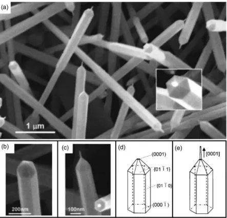
The morphology of the as-prepared film was examined with field-emission scanning electron microscopy共SEM兲. As shown in Fig. 1共a兲, well-hexagonal faceted nanopencils with uniform size were grown on the substrate. The penholders have an average diameter of 200 nm and the pen tips on the top are in a range of 20–30 nm in diameter. An enlarged view of a pen tip is shown in the inset of Fig. 1共a兲, exhibiting the hexagonal prismatic morphology.
Here, we propose a two-stage growth mechanism for the nanopencils in the following. The first stage was involved with the growth of the hexagonal penholders along the 关0001兴 direction. The morphology was fully consistent with the growth habit of the ZnO ideal crystal model12in that the relative crystal growth velocity should follow the sequence as: V具0001典⬎V具011¯0典⬎V具0001¯典. Figure 1共b兲 shows the SEM im-age of a penholder alone for the first stim-age and Fig. 1共d兲 is the respective schematic diagram showing the idealized growth habit. Because no catalysts were found, the growth is different from the traditional vapor-liquid-solid mechanism. The penholders were suggested to nucleate via a self-catalyzed mechanism. Subsequently, the second stage was
a兲Author to whom correspondence should be addressed; also at: Center for
Micro/nano Technology Research, National Cheng Kung University, Tainan 70101, Taiwan; electronic mail: [email protected]
APPLIED PHYSICS LETTERS 87, 013110共2005兲
0003-6951/2005/87共1兲/013110/3/$22.50 87, 013110-1 © 2005 American Institute of Physics
involved with the growth of the narrow pen tips on the top. The nanotips occurred when the working pressure was de-creased suddenly at the beginning of the slow cooling pro-cess. Under this condition, the prism growth may stop due to the shortage of the source vapor. However the zinc source still evaporated with a slower rate during the cooling pro-cess, the共0001兲 platform on the top of the prism could act as an ideal site for the second nucleation. Owing to the continu-ously decreasing zinc vapor pressure with decreasing tem-perature, most pen tips possess needlelike morphologies. Figure 1共c兲 is the SEM image of a nanopencil, while Fig. 1共e兲 shows the respective schematic growth mechanism of the pen tips. Besides, the fact that the area of the 共0001兲 platforms decreased with the diameter of the penholders共not shown here兲 indicates that the nucleation size of the pen tips is determined by the size of the共0001兲 platform area.
The detailed microstructures of the ZnO nanopencils were characterized using a JEOL 2100 field emission trans-mission electron microscope共TEM兲. Fig. 2共a兲 shows a low-magnification TEM image of a nanopencil that has sharp pen tip morphology. The subtended half-angle关as defined in Fig. 2共e兲兴 at the tip is as small as 4° , showing an ideal configu-ration for field emission application. An electron diffraction pattern and high-resolution TEM image of a nanopencil in Figs. 2共b兲 and 2共c兲 exhibit the characteristics of single crystal growing along the关0001兴 direction. A typical high-resolution TEM image of the pen tip in Fig. 2共d兲 presents numerous surface perturbations with just 2–5 nm in size indicated by arrows. These nanosized perturbations are epitaxially con-nected with the needlelike tip body, which has been sug-gested to enhance field-emission performance.13
Field-emission measurements were carried out by a two-parallel-plate configuration in a vacuum chamber with pres-sure ⬍5⫻10−6 Torr. The indium-tin oxide film coated on glass was used as an anode and the Si substrate with the as-deposited ZnO nanopencils as a cathode. The distance
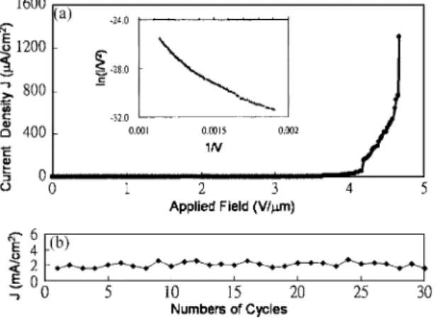
be-tween the electrodes was 214m. The emission current was measured by applying a voltage increasing from 1 to 1000 V with a sweep step of 5 V. Here, we define the turn on field as the electric field required to produce a current density of 10A / cm2. The results shown in Fig. 3共a兲 indicate that the ZnO nanopencils have a turn on field of 3.7 V /m, which is higher than CNTs1and lower than other semiconductors2,3,5–7 and previously measured ZnO nanostructures.4,8,9,14–16 The current density is 1.3 mA at 4.6 V /m and shows no satu-ration. The corresponding Fowler–Nordheim共F–N兲 plot17 is shown in the inset of Fig. 3共a兲, which exhibits a nonlinear behavior with a slightly larger slope at a higher applied elec-tric field, where the slope transition occurs at 3.3 V /m. At this low applied electric field, the transition is not caused by a vacuum arc phenomenon since no fusion was found on the FIG. 1.共a兲 Low magnification SEM image of the nan-opencils, showing pen tips on the nanopencils with the inset for an enlarged view of a pen tip;共b兲 SEM image of a penholder;共c兲 SEM image of a nanopencil with a pen tip; 共d兲 the schematic idealized growth habit of ZnO; and共e兲 the schematic growth mechanism of a pen tip.
FIG. 2. 共a兲 TEM image of a nanopencil; 共b兲 electron diffraction pattern taken from the nanopencil shown in共a兲; 共c兲 high-resolution TEM image of a nanopencil;共d兲 TEM image of a pen tip; and 共e兲 an enlarged view of the pen tip shown in共a兲, revealing the initial half-angle of the tip is around 4°.
013110-2 Wang et al. Appl. Phys. Lett. 87, 013110共2005兲
nanopencils according to SEM. In addition, it does not seem to be defect-related phenomenon because of the good crys-tallinity of the ZnO nanopencils revealed by TEM. There-fore, the two-slope F–N curve may be contributed by two types of field emitters with distinct geometrical factors acti-vated simultaneously at different applied electric fields, which should correspond to the pen tips as well as numerous nanosized surface perturbations on the side faces consistent with the TEM observations. The above discussion was veri-fied by a simple calculation which showed that the total emission current can be fitted very well by two independent curves from two types of field emitters with distinct geo-metrical factor.
From the averaged slope of the F–N plot, the field en-hancement factorof the ZnO nanopencils was estimated to be about 2300 by assuming the work function of ⌽ = 5.3 eV,11which is good enough for various applications of field emission. The average  of the ZnO nanopencils is related to the geometry, structure, and density of nanopencils grown on the substrate. The grown nanopencils exhibit high crystalline quality and sharp tips with nanosized surface per-turbations, resulting in a high field enhancement factor. Fur-thermore, the nanopencils could be subjected to the field emission test at least 30 times under the sweeping electric field from 0 to 5 V /m without obvious changes in the re-sults. Figure 3共b兲 shows the current density reproducibility at
an electric field of 5 V /m. The average current density was 2.1 mA.
In summary, ZnO single-crystal nanopencils were syn-thesized via a simple two-step pressure controlled thermal evaporation without catalysts at a low temperature of 550 ° C. Low electric field emissions indicate that the ZnO nan-opencils are promising for the application in field emission microelectronic devices.
The work was supported by Research Grant No. NSC93-2120-M-006-007, National Science Council of Taiwan. The authors are grateful to Professor Y.-C. Chen for helpful dis-cussions. The assistance from K. H. Liao for the field-emission is also greatly appreciated. The authors thank the Center for Micro/nano Technology Research, National Cheng Kung University, Taiwan for the provision of HR-TEM.
1J.-M. Bonard, C. Mirko, K. Christian, K. Ralph, N. Olivier, and W.
Nico-las, Carbon 40, 1715共2002兲.
2Y.-H. Lee, C.-H. Choi, Y.-T. Jang, E.-K. Kim, and B.-K. Ju, Appl. Phys.
Lett. 81, 745共2002兲.
3K. W. Wong, X. T. Zhou, F. C. K. Au, K. L. Lai, C. S. Lee, and S. T. Lee,
Appl. Phys. Lett. 75, 2918共1999兲.
4Y.-K. Tseng, C.-J. Huang, H.-M. Cheng, I.-N. Lin, K.-S. Liu, and I.-C.
Chen, Adv. Funct. Mater. 13, 811共2003兲.
5Y. B. Li, Y. Bando, and D. Golberg, and K. Kurashima, Appl. Phys. Lett.
81, 5048共2002兲.
6V. N. Tondare, C. Balasubramanian, S. V. Shende, D. S. Joag, V P.
God-bole, and S. V. Bhoraskara, Appl. Phys. Lett. 80, 4813共2002兲.
7J. Chen, S. Z. Deng, N. S. Xu, S. Wang, X. Wen, S. Yang, C. Yang, J.
Wang, and W. Ge, Appl. Phys. Lett. 80, 3620共2002兲.
8C. J. Lee, T. J. Lee, S. C. Lyu, and Y. Zhang, Appl. Phys. Lett. 81, 3648
共2002兲.
9Y. W. Zhu, H. Z. Zhang, X. C. Sun, S. Q. Feng, J. Xu, Q. Zhao, B. Xiang,
R. M. Wang, and D. P. Yu, Appl. Phys. Lett. 83, 144共2003兲.
10Q. Wan, K. Yu, T. H. Wang, and C. L. Lin, Appl. Phys. Lett. 83, 2253
共2003兲.
11L. Dong, J. Jiao, D. W. Tuggle, J. M. Petty, S. A. Elliff, and M. Coulter,
Appl. Phys. Lett. 82, 1096共2003兲.
12W.-J. Li, E.-W. Shi, W.-Z. Zhong, and Z.-W. Yin, J. Cryst. Growth 203,
186共1999兲.
13Y. B. Li, Y. Bando, and D. Golberg, Appl. Phys. Lett. 84, 3603共2004兲. 14S. H. Jo, J. Y. Lao, and Z. F. Ren, Appl. Phys. Lett. 83, 4821共2003兲. 15T. Y. Kim, J. Y. Kim, S. H. Lee, H. W. Shim, S. H. Lee, E. K. Suh, and K.
S. Nahm, Synth. Met. 144, 61共2003兲.
16Q. H. Li, Q. Wan, Y. J. Chen, and T. H. Wang, Appl. Phys. Lett. 85, 636
共2004兲.
17R. H. Fowler and L. W. Nordheim, Proc. R. Soc. London, Ser. A 119, 173
共1928兲. FIG. 3. Field-emission measurements of the ZnO nanopencils.共a兲 Current
density-electric field characteristics with the inset for the corresponding F–N plot.共b兲 Current density reproducibility recorded at an applied field of 5 V /m.
013110-3 Wang et al. Appl. Phys. Lett. 87, 013110共2005兲