A Novel ZVS-ZCS Bidirectional DC-DC Converter For Fuel Cell And Battery Application
V.V.SUBRAHMANYA KUMAR BHAJANA Research scholar, EEE department
Bharath University Chennai, India [email protected]
S.RAMA REDDY Professor, EEE Department.
Jerusalem College of engineering Chennai, India
Abstract— A new ZVS-ZCS bidirectional DC-DC converter is proposed, which provides high output voltages 80v-180v. With proposed ZVS-ZCS concept, the MATLAB simulation results of the application to a fuel cell and battery application have been obtained and compared with those of ZVS bidirectional and applications in order to show the excellent performance of the proposed concept. In addition to this experimental setup has been developed. The experimental results are compared with the simulation results.
Keywords-component; ZVS,ZCS,TDR,DC-DC converter.
I. INTRODUCTION
In recent years, the area of bidirectional DC-DC converters is improving the fuel cell economy, automobile companies are developing alternative battery operated vehicles. In addition, a major change in the electrical system of the vehicles is on the horizon by going for a 40 to 300V DC from 12/24v DC systems. The main reasons for switching over to 12v/24v to 300v are to meet the increased electrical demands of cell vehicles, to lower the current drawn from the battery, and to implement additional safety and comfort features, also to reduce the mechanical and hydraulic components, and to improve the design flexibility of the vehicles. In hybrid/fuel cell vehicles, the main goals are to have a high efficient, small size, rugged and low cost bidirectional DC-DC converter. In hybrid/fuel cell vehicles, a power conditioning unit such as novel bidirectional DC-DC converter to match the fuel cell voltage with the battery pack may also required. In certain conditions, a fast response required to supply load, converter to give bidirectional power to that vehicle system without any disturbance. It is able to operate at adverse environmental conditions. The power semiconductor devices (MOSFET, IGBT, etc) and packaging of the individual units and the system integration play a major role in hybrid/fuel cell vehicles. The proposed converter system should be efficient to improve the range of performance of the battery operated vehicles. In addition to the power semiconductor devices, controllers, there are several other components such as inductors, capacitors, isolation transformer form a major portion of the proposed system. The soft switching converters have the advantage of lower switching losses and higher operating voltage. Hence the proposed soft switching techniques ZVS/ZCS were needed. The proposed system with two integrated function is that DC/AC and AC/DC conversion,
with low losses and with minimum use of capacitors need to be developed.
This paper presents a novel ZVS-ZCS bi-directional DC- DC converter. The new converter is based on a dual half-bridge topology with an auxiliary circuit in primary side. It has the advantages like low EMI, low switching stresses, low switching losses compared with ZVS bi-directional DC-DC converter. The ZCS topology removes the turn-off current tail of the main switch. The ZCS operation is obtained by both forcing the primary current towards zero and delaying its raise, or by resetting the primary current before the corresponding switch turned off. The ZVS-ZCS bi-directional DC-DC converter has been simulated and developed for rectification and inversion operations in both buck and boost. The operating modes of the proposed converter are described in the following section. The obtained results shows that the proposed converter can be a good solution for fuel cell vehicle systems, where voltage boosts and efficiency are key issues. The simulations were conducted with the switching frequencies of 10 KHz. The current waveforms at the DC-AC stages are observed to be conformity with the theoretical estimates.
II POWER STAGE DESCRIPTION AND OPERATION A. power stage description
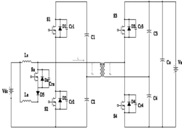
The proposed bi-directional DC-DC converter for fuel cell and battery applications is shown in Fig. 2. In the ZVS bidirectional DC-DC converter[1] low-voltage side half-bridge with MOSFETS and high voltage side half bridge with IGBTs were developed. Where as in the proposed ZVS-ZCS bidirectional DC-DC converter, dual half-bridges are developed using MOSFETs with an auxiliary circuit in the low voltage side. The auxiliary circuit used in this converter has been adapted from [6] and it can also be used in full-bridge topologies, but this will be the scope of future work. In proposed ZVS-ZCS bidirectional DC-DC converter the auxiliary circuit is composed of one resonant inductor La, one auxiliary switch Sa, and also diode Da, so that the zero current switching (ZCS) in main switches S1& S2 can be obtained.
Switch Sa is turned on under zero current switching (ZCS) condition. When power flows from the low voltage side to high voltage side, the circuit works in ZCS condition to turned off and ZVS condition to turned on of a main switches S1, S2
in boost mode. In the other direction of power flow, the circuit operates in ZVS condition (buck mode). The transformer is used to provide isolation and voltage matching. The leakage inductance of the transformer is utilized as an interface and energy transfer element between two half-bridges. The two voltage source half-bridges each generates a square wave voltage applied to the primary and secondary of the transformer, respectively. The major draw back of this converter is TDR penalty because auxiliary circuit used in primary side. The TDR of the [1] ZVS bidirectional DC-DC converter is calculated as TDR = 2Vdc. Iac. (2 devices) = 4 Po,
where Po is the output power. The TDR of the proposed ZVS- ZCS bidirectional DC-DC converter is calculated as TDRP = 2Vdc. Iac. (3 devices) = 6 Po, Where Po is again the output power. The TDR has been increased for the proposed converter and the ZVS bidirectional DC-DC converter is not same output power. The main advantage of proposed circuit is the current stresses are reduced for the low voltage side main switches S1 and S2 and high efficiency is achieved due to ZCS condition.
Fig.1. ZVS bidirectional DC-DC converter
B. Description of operating stages
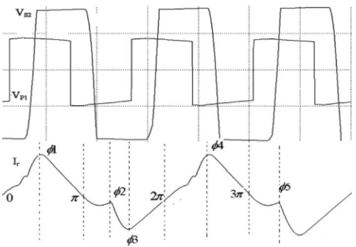
Fig. 2. illustrates the proposed converter topology and the commutation waveforms in boost mode. ZCS is achieved by auxiliary circuit used in one half-bridge, operating the two half-bridges with a phase shift. The circuit operation that is significant for the development of the state space model. Fig.
2 is the proposed circuit. Fig. 3 presents the voltage and current waveforms of the transformer during one switching period. In fuel cell applications, when power flows from the low voltage side to high voltage side, the circuit works in boost mode to keep the high voltage at a desired high value before fuel cell can generate power. In other direction of power flow, the circuit works in buck mode to absorb regenerated energy. Based on the waveforms in Fig. 3, there are six operation modes in one switching cycle, and the
transformer current ir of each mode can be calculated as follows:
Fig. 2. Proposed ZVS-ZCS bidirectional DC-DC converter
Mode I: ir = (v1+v4)θ / ω Ls + ir (0) (1) Mode II: ir = (v1-v3) (θ -φ1) / ω Ls + ir (φ1) (2)
Mode III: ir = 0 (3)
Mode IV: ir = - (v2+v3) (θ -π) / ω Ls + ir (π) (4) Mode V: ir = - (v2+v4) (θ -π-φ) / ω Ls + ir (π+φ1) (5)
Mode VI: ir = 0 (6)
The current initial conditions can be solved using the boundary conditions of
ir(0) = ir(π)=0 (7)
ir(φ1) = -ir(π+φ1) (8)
Further, the output power can be found to be
Ts is the period of switching frequency, Vdc is the input voltage in boost mode. The output power can be regulated by phase shift angle ø1, duty cycle and switching frequency ω. If duty cycle assumed to 50% then the output power equation can be simplified as
Po= x T0/ s = Vdc2/ ωLs [(ø2- π) ø1/ π)]……… (9) Because of the asymmetry property of dual half-bridges, the operation principles of boost mode and buck mode are not the same, polarity of the phase shift angle is also not same.
1. Boost mode:
The interval of Fig. 3. describes the various stages of operation during switching period in boost mode. The converter operation is repetitive in the switching cycle. One complete cycle is divided into six steps. To aid in understanding each step, a set of corresponding annotated circuit diagrams is given in Fig. 4(a,b,c,d,e,f) with a brief description.
Fig. 3. Voltage and current waveforms of transformer during boost mode
First stage (0 to φ1): switch S1 starts to conduct. Due to the resonant capacitor Cr1 , the voltage across S1 is becomes zero.
During this stage C1, C4 are charged, C2, C3 are discharged.
Fig. 4(a) first stage(0 to φ1)
Second stage (φ1 toπ): S1 is still turn on state. During this stage C1, C4 are charged, energy stored in C2, C3 are transferred to the load. When ir reaches at φ3, Sa is gated to turn off S1. This stage finishes when S1 is turned off.
Fig .4(b) second stage(φ1 to φ3)
Third stage (π to φ2): at this stage Sa is turn on, remaining switches are in off state. During this stage energy stored in C1,C4 are transferred to the load. C3, C2 are charged.
Fig. 4(c). third stage(φ3 to π)
Fourth stage (φ2 to 2π): when S2 is turned on, C2 & C3 are charged, C3 & C4 discharged. This stage finishes when Sis turned-on.
Fig. 4(d) fourth stage(π toφ4)
Fifth stage (2π to 3π): At this stage S2 is still in turn on state.
During this stage C2, C3 are charged, energy stored in C1, C4
are transferred to the load. When ir reaches at 3π, Sa is turned on to turn-off the S2. This stage finishes when S2 is turned off.
Fig . 4(e) fifth stage( 3π to φ5)
Sixth stage (3π to φ5): at this stage Sa is turned on, remaining switches S1&S2 are in off state. During this stage energy stored in C2, C3 transferred to the load. C1, C4 are charged.
Fig.4(f) sixth stage( 3π to φ5) 2. Buck mode:
Because of the auxiliary circuit in one half-bridge the two sides are asymmetrical, the operation principles in buck mode are similar to those in boost mode except mode III
& mode VI. Due to the reversed power-flow direction, the phase of the VS2 is leading than VP1. The inductor current LS is reversed. The buck mode only operates under ZVS condition.
This mode of operation can be divided into four steps. In this mode the switches in S3 &S4 are turned on and turned off at zero voltage due to the resonant capacitors Cr3, Cr4.Body diodes of the switches S1& S2 acts as rectification.
Mode I: ir = (v3+v4)θ / ω Ls + ir(0) (10) Mode II: ir = (v3-v2) (θ -φ1) / ω Ls + ir (φ1) (11) Mode III: ir = - (v1+v4) (θ -π) / ω Ls + ir (π) (12) Mode IV: ir = (- v2+v4) (θ -π-φ) / ω Ls + ir (π+φ1) (13)
III. STATE SPACE MATHEMATICAL MODEL
The state variables of the proposed converter [1] are chosen to be the inductor currents i1, i2, transformer current ir
and the capacitor voltages v1, v2, v3 and v4 [1] that state variables vary slowly with time, also does i1,i2 if enough large inductance and small inductances are selected, while the state variable ir varies quickly with time.
To analyze the behavior of the fast variable ir, the other slow state variables can be treated as dc constants. From section II, we know that the converter is operated as dual active half-bridges and there are six operation modes during one switching cycle. With the help of switching functions, the state equation of the slow state variables is described by
1 [vd c i R1 b P v1( 1 v2 )] /Ld c
i• = − − + (14)
1 1 2
1/ [a b b a( )]
a L v i R S v v
i• = − − − (15)
1 1 1
1 P i( /r Cp) P i( /Cp)
v• = − + (16)
1 1 1
2 ir(1 P ) /Cp P i( /Cp)
v• = − + (17)
3 4 1 0 3 4 2
3
3 4 0 3 4 2
[ ( ) / ( ) / )](1 ) /
[ ( ) / ( ) ] /
s S S
r s s s
v v v P R C d v v dt P C
i v v v R C d v v dt P C
v• = − + − − + + −
+ − + − − +
(18)
3 4 0 3 4 2
4
3 4 0 3 4 2
[( ( ) / ( ) / )](1 ) /
[ ( ) / ( ) ] /
r s S S
s s s
i v v v R C d v v dt P C
v v v R C d v v dt P C
v• = − + + − + + −
+ − + − − +
(19) Where Cp= C1=C2 and Cs= C3=C4.
These equations describe all the operation modes of one switching cycle in Fig. 3.The next step is to calculate the integration of fast variable ir in [0, ø 1] ,[ ø1, π],[π,ø2],[ø2,ø3,],
[ø3,2π] ,respectively based on (1)(2)(3)(4)(5)(6). Then substitute the above results and switch functions P1and P2 in to (14)(15)(16)(17)(18)(19) to calculate the move averages of the slow variables shown in (20)
1 1
1 1 2 2
3 3 1 1
2
( ) / ; ( ) /
( ) / ; ( ) /
( ) / ; ( ) /
a a
t Ts
t
t Ts t Ts
t t
t Ts t Ts
t t
i avg i dt Ts i avg i dt Ts v avg v dt Ts v avg i dt Ts
v avg v dt Ts i avg i Ts
φ π +
+ +
+ +
= =
= =
= =
∫ ∫
∫ ∫
∫ ∫
(20)
The state space model of proposed converter with ZCS condition is derived.
We shall now demonstrate the normal operation of the ZVS- ZCS bidirectional DC-DC converter through simulation using MATLAB/Simulink. The simulation results are shown in Fig.
3, 5(a, b)and Fig. 6.
Fig .5a. Transformer primary and secondary side voltages in boost mode
IV SIMULATION RESULTS
The detailed circuit model is built using Matlab/Simulink. The simulated results are compared with ZVS-bidirectional DC- DC converter to show the performance of proposed converter.
1. Boost mode: The following parameters are selected according to a 400W for fuel cell and battery applications.
Vb =12V, Rb=1Ω, D = 45%, fs=10 kHz, Ls= 380 µH, La= 4.96µH, CP1= CS1= 20mF, C0= 150mF, RL= 0.5Ω.Vo= 80V The simulations revealed modes of operation where the primary side switches operate under ZVS, ZCS conditions.
The simulation results were shown in Fig. 3, 5(a,b).
Fig. 5b. DC output voltage
2. Buck mode: Similarly, the buck mode can also be simulated using same parameters as boost mode. Simulations of the proposed converter waveforms are presented in Fig. 6. Shown are the primary side and secondary side voltages (VP1, VS2).
The simulations revealed modes of operation where the primary side switches operate under ZVS condition.
Fig. 6. Transformer primary and secondary voltages in buck mode
V Experimental Results
An experimental setup of the proposed converter has been built to verify the principle of operation. It was operated with both boost mode with a ZVS-ZCS and buck mode with the ZVS technique. The experimental setup is pictured in Fig. 7a.
The specifications are as follows.
• Rated output power: PO = 80W
• Input voltage: Vin = 12V
• Output voltage: VO = 80V
• Switching frequency: fs = 10kHz
• Maximum duty cycle: Dmax = 0.5
• Transformer turns ratio: N1:N2 = 1:2
The 80W converter which was tested in the laboratory was designed with a output voltage 80V and was driven from a half-bridge with an auxiliary circuit.
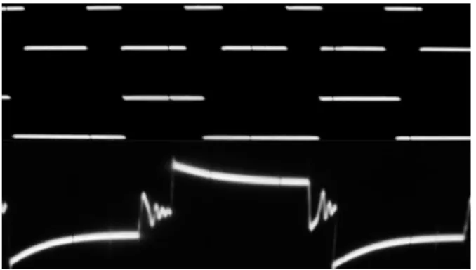
The oscillograms in Fig. 7b shows primary side and secondary side voltages in boost mode, and Fig. 7c shows the driving pulses to the switches S1,Sa and the transformer current (ir) which shows that ZCS state in boost mode. The converter did not behave as expected due to the circuit layout and component selection. The rated input voltage is 12V and output voltage 80 V / 80W is due to a 1:2 turns ratio for the transformer. Instead of using IGBTs in secondary side [1],IRF 840 MOSFETs are used in secondary side. An additional advantage of the auxiliary circuit is that switching losses of S1&S2 is reduced.
Fig. 7a. Experimental setup
Fig driving pulses
Fig. 7b. Primary side and Secondary side voltages in boost mode
Fig. 7c. Driving pulses Sa& S1 and Transformer current ir
VI CONCLUSION
A novel ZVS-ZCS bi-directional DC-DC converter has been presented in this paper. The operation, state space mathematical model and experimental results were illustrated.
Simulation results are compared with the experimental results to verify the operation principle.
It is shown that ZVS-ZCS in one direction of power flow is achieved in boost mode with no switching losses involved and other direction of power flow involves ZVS with no switching losses. Due to the simultaneous boost conversion and inversion provided by the low voltage side half bridge, current stresses on the switching devices and transformer are reduced by switching an auxiliary switch in primary side i.e.
ZCS condition. The advantages of the proposed circuit are, current stresses are reduced, high efficiency, which is achieved due to the ZCS operation. The drawbacks of this proposed converter is cost is increment due to the auxiliary circuit components and decreased output power. This proposed converter for medium power applications like fuel cell and battery, with high power density. Excellent dynamic performance is obtained because of the auxiliary circuit used in the half bridge.
ACKNOWLEDGMENT
The authors wishes to thank Mr Uday kumar for his help in fabrication at the initial stages. We are also grateful to Mr. Srinivas Rao Kureti for his simulation assistance in this work and Mr.K.Rama Lingeswara Prasad his assistance.
REFERENCES
[1] Fang Z.Peng,Hui Li,Gui-Jia,Jack S.Lawler, “A new ZVS bidirectional dc- dc converters for fuel cell and battery application,” IEEE Trans. Power Electro., vol. 19,No. 1,Jan 2004,pp 54-65.
[2] H.L.Chan, K.Cheng, and D.Sutanto, “ An extended load range ZCS-ZVS bidirectional phase shift dc-dc converter,” in proc. 8th Int.conf.Power Electron. Variable speed drives, 2000, pp 74-79.
[3] Manu Jain, M.Daniele, and Praveen K.Jain, “ A bidirectional dc-dc converter topology for low power application,” IEEE Trans. Power Electro.,vol. 15, No.4,July 2000,pp 595-606
[4] Fang Z.Peng,Hui Li, “modeling of a new ZVS bidirectional dc-dc converter,” IEEE Trans. Power Electron, vol. 40, No. 1, Jan 2004, pp 272- 283.
[5] H.Chung et al.,” A ZCS bidirectional flyback dc-dc converter,” IEEE Trans. Power Electron, vol. 19,No. 6, Nov 2004, pp 1426-1434.
[6] R.Mendes Finzi Neto,F.Lessa Tofoli, and Luis carlos de Freitas, “ A High power-factor half-bridge doubler boost converter without commutation losses,” IEEE Trans.Power Electron, vol. 52, No. 5, Oct 2005, pp 1278-1285.
[7] L.C.Freitas, D. F. Cruz, and V.J. Farias,” A novel ZCS-ZVS PWM dc-dc converter for high switching frequency: analysis,simulation and experimental results,” in proc.IEEE APEC’93,San Diego,CA,1993, pp 693-699.
[8] F.Carichhi, F.Crescimbini, F.G.Capponi, and L.Solero,” Study of bidirectional buck-boost converter topologies for application in electrical vehicle motor drives,” in proc. IEEE applied power electronics specialists conf. Expo, 1998, pp. 287-293.
[9] S.Hamada et al.,” A novel zero-voltage and zero-current switching PWM dc-dc converter with reduced conduction losses,” IEEE Trans. Power electron., vol. 17, pp. 413-419, May 2002.
[10] Z.R.Martinez and B.Ray,” Bidirectional dc/dc power conversion using constant frequency multi-resonant topology,” in Proc. APEC’94, 1994, pp.
991-997.\
[11] D.Makasimovic, S.Cuk, “ A general approach to synthesis and analysis of quasi-resonant converters,” IEEE Trans.Power Electron., vol. 6,No. 1,Jan 1991, pp. 127-140.
[12] R. L. Lin, Fred C.Lee,”Novel zero-current switching-zero-voltage switching converters,” in proc. IEEE PESC’96, pp. 438-442.
[13] R. W. DeDonker, D. M. Divan, and M.H.Kheraluwala, “ A Three-phase soft-switched high power density dc-dc converter for high power applications,” IEEE Trans. Ind.Applicat.,vol. 27,pp.. 63-73,Jan./Feb.1991.
V.V.SUBRAHMANYA KUMAR BHAJANA received his B.E. degree in Electronics and Communication Engineering from Sapthagiri College of Engineering, Dharmapuri, Tamilnadu, India (University Of Madras), in 2000 and there after, he did his M.E degree in Power Electronics and Drives from the P.S.N.A College of engineering and Technology, Dindigul, Tamilnadu, India under Anna University, Chennai in the year 2005. He is presently a research scholar at Bharath University Chennai, India. His key area of interest is Power Electronics engineering, which includes soft switching DC - DC converters and their applications.
S.RAMA REDDY is professor of electrical department, Jerusalem engineering college, Chennai, tamilnadu, India. He obtained his L.E.E. from S.M.V.M.ploytechnic, Tanuku, A.P, A.M.I..E. in electrical engineering from institution of engineers (India), M.E. in Power Systems from Anna University. He has published over 20 technical papers in national and international conference proceedings/journals. He has secured A.M.I.E. institution gold medal for obtaining highest marks. He has secured Aimo best project award and Vijaya Ratna Award. He has worked in Tata Consulting Engineers, Banglore and Anna University, Chennai. He has teaching experience of 12 years. His research interest is in the areas of resonant converters, VLSI , and solid state drives. He is life member of institution of engineers (India), Indian society for technical education, system society of India and society of power engineers. He is a fellow of institution of electronics and telecommunication engineers ( India).
He has published text books on power electronics and solid state circuits.