Effect of Formal Passivations on Temperature-Dependent
Characteristics of High Electron Mobility Transistors
Po-Hsien Lai,a Rong-Chau Liu,bSsu-I Fu,aYan-Ying Tsai,aChing-Wen Hung,a Tzu-Pin Chen,aand Wen-Chau Liua,z
a
Institute of Microelectronics, Department of Electrical Engineering, National Cheng-Kung University, Tainan, Taiwan 70101
b
Chung Shan Institute of Science and Technology, Lung-Tan, Tao-Yuan, Taiwan 32544
Temperature-dependent characteristics of high electron mobility transistors共HEMTs兲 with sulfur and SiNxpassivations are
com-prehensively studied and demonstrated. Experimentally, for the studied device with formal passivations, better dc and microwave characteristics are obtained over a wide operating temperature range. In particular, as compared with the device only with sulfur passivation, the slight degradations of device performance are caused by the temperature stress during the deposition of SiNxlayer
and presence of surface traps at the SiNx/AlGaAs interface. However, under an accelerated stress test, this formal-passivated
device shows improved reliability performance. Based on these good results, the formal-passivated HEMT is expected to exhibit relatively better long-term operation stability and reliable device characteristics.
© 2007 The Electrochemical Society. 关DOI: 10.1149/1.2409479兴 All rights reserved.
Manuscript submitted September 6, 2006; revised manuscript received October 9, 2006. Available electronically January 5, 2007.
Recently, high electron mobility transistors共HEMTs兲 have been applied widely in high-performance microwave and power circuits.1-3 It is known that, practically, the manufacturing cost, yield, device reliability, and longevity are mandatory factors for sys-tem applications. Because metal-semiconductor 共MS兲-based struc-tures are widely employed in III-V HEMTs, the surface effect in-duced by high density of interface traps at MS contacts has attracted much attention. The surface effects crucially influence device per-formance because the electron transport within channel layer is strongly affected by the air-exposed surface region.4Hence, the lack of an adequate surface passivation usually results in the formation of native oxide and degradation of electrical properties. To optimize device behaviors and achieve thermal stability, the sulfur passivation has been developing as a promising technique.5-7
Previously, the sulfur passivation effects on the temperature-dependent characteristics of HEMTs with Pt/Au gate Schottky con-tact were demonstrated in our report.7However, the Pt metal is easy to chemically react with GaAs or AlGaAs layer at the relatively low temperature.8Thus, it is difficult to control the accuracy and preci-sion of sulfur passivation on the device with Pt/Au gate alloy. Also, the sulfur passivation effect could be degraded quickly when the device was exposed to ambient atmosphere.9This certainly leads to reliability problems for device performance. Therefore, deposition of an oxygen-free dielectric layer after sulfur passivation is neces-sary to protect the sulfide layer and achieve long-term stable passi-vation. Above all, silicon nitride共SiNx兲 is one of the dominant ma-terials for further stabilizing the sulfur passivation effect.10,11
In this work, a formal passivation method that combines the sulfur and SiNxpassivations is employed to achieve improved op-eration stability and reliable device performance in HEMTs with Ti/Pt/Au gate Schottky contact. To meet the desired accuracy, the Ti metal as a part of gate Schottky contact is employed.12This im-proved experimental condition would be useful to study the inherent effect of sulfur and SiNx passivations without any unpredictable effects. Moreover, the proposed passivation technique is substan-tially different from previous work.7For the formal passivation, an additional SiNxpassivation layer is deposited on the mesa sidewall and the exposed sulfur-passivated barrier surface between drain-source and gate edge. The effects of sulfur and SiNxpassivations in the electric parameters are analyzed and comprehensively studied. The comparisons between the formal-passivated device and nonpas-sivated device are made to show the effect of formal passivation on device performance. Furthermore, in order to demonstrate the
supe-riority of the proposed formal passivation over standard sulfur pas-sivation, the sulfur-passivated device is also included in the reliabil-ity test.
Experimental
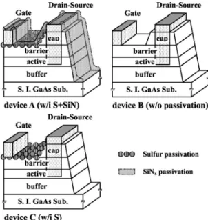
The studied device was grown on a 共100兲-oriented semi-insulating共S.I.兲 GaAs substrate by a metallorganic chemical vapor deposition 共MOCVD兲 system. The epitaxial structure consisted of buffer, active, barrier, and cap layers. The conventional HEMT structure with an n-Al0.25Ga0.75As 共n = 3 ⫻ 1017cm−3兲 barrier layer is similar to the previous work.7 The Hall measurement showed the electron mobility共n兲 of 6342 cm2/V s and sheet carrier density共ns兲 of 2.51 ⫻ 1012cm−2at 300 K. The upper barrier layer provides good Schottky characteristics, and the lower buffer layer suppresses the substrate leakage current through the substrate leak-age path. After epitaxial growth, the mesa isolation was performed by wet chemical etching process. Drain-source ohmic contacts were formed on the top of the cap layer by rapid thermal annealing of AuGe/Ni/Au metallurgy. Then, the cap layer was removed. The de-tailed formal passivation process is expressed as follows. First, pho-toresist was patterned to define the exposed drain-source region. Prior to gate metal deposition, the sample was immediately passi-vated by soaking in the ammonia-sulfide关共NH4兲2Sx, 5%兴 solution for 10 min at room temperature. Subsequently, the sample was rinsed in acetone and deionized共DI兲 water, followed by blown dry N2gas. Although the S-III bonds were formed on the AlGaAs sur-face, the different thin, whitish, amorphous sulfur and sulfates were found on the drain and source electrodes.13However, by using this particular procedure, it could prepare the clean surfaces of AlGaAs barrier layer and ohmic contact metal. Finally, gate Schottky con-tacts with the gate length of 1m were achieved by evaporating Ti/Pt/Au metal on the AlGaAs barrier layer. After gate metalliza-tion, the remaining barrier surfaces of sulfur-passivated AlGaAs layer between gate and drain-source electrodes were air exposed. To protect the sulfur-passivated AlGaAs surface from direct exposure to the ambient atmosphere, the SiNx共⬃50 nm兲 layer was deposited on the sample共device A兲 by plasma-enhanced chemical vapor deposi-tion 共PECVD兲 at 573 K. For comparison, device B 共without any passivation兲 and device C 共only with sulfur passivation兲 are also fabricated by the same process of device A except for surface pas-sivation. The schematic illustrations of different passivations on the studied devices are depicted in Fig. 1. The used gate dimension is 1⫻ 100 m2. In addition, the spacing between the drain and gate electrodes is 3m.
z
Results and Discussion
Figure 2 shows the gate-drain breakdown voltage共BVGD兲 and Schottky barrier height 共⌽B兲 as a function of temperature. The source terminal is floating. The BVGDvalues are measured under the
IG= −1 mA/mm. The BVGDvalues of devices A, B, and C are 39.3, 35.9, and 40.8 V at 300 K. Even the operating temperature is el-evated up to 480 K; the improved BVGDvalues of 27.6 and 28.6 V are obtained for devices A and C, which are substantially higher than that of 23.1 V for device B. Especially, device A shows the BVGD slightly decreased than device C. This is because the temperature stress involved in SiNxlayer deposition could cause the degenera-tion of gate Schottky and breakdown characteristics.10,11Besides, it is suggested that the increased gate leakage current as well as dete-riorated breakdown behaviors are dominated by the generation-recombination共G-R兲 current.10For the device studied without any passivation 共device B兲, the interface traps at the AlGaAs barrier surface would produce a G-R leakage current path and result in the reduced BVGD.14Hence, the relatively lower BVGD of device B is
observed. The corresponding temperature coefficients, i.e., 共BVGD/BVGD兲共1/T兲, of devices A, B, and C are −1.66 ⫻ 10−3, −1.89⫻ 10−3, and −1.52⫻ 10−3/K, respectively, over the tempera-ture range from 300 to 480 K. Due to the lower thermal conductiv-ity of SiNxlayer,15the temperature coefficient of device A is slightly degraded as compared with that of device C. However, both devices A and C reveal lower temperature coefficients of performance deg-radation. This is attributed to the formation of stable S-III bonds on the sulfur-passivated AlGaAs surface, which can suppress the inter-face traps and corresponding leakage current among a wide range of operating temperature.14,16
According to the thermionic emission model and modified Norde method, the conducting current of an ideal gate Schottky character-istic and Norde function can be given as17,18
I共V兲 = AA*T2exp
冉
−q⌽B kT冊
exp冋
q共V − IR兲 nkT册
关1兴 and F共V,␥兲 = V/␥ − kT q ln冋
I共V兲 AA*T2册
关2兴where A is the area of Schottky contacts, A*the effective Richardson constant, k the Boltzmann’s constant, T the absolute temperature, R the series resistance, and␥ the arbitrary constant greater than n, respectively. The modified Norde method is used to overcome the related series resistance created by the Al0.25Ga0.75As barrier layer. The calculated⌽B共n兲 values of devices A and B are decreased from 0.993 and 0.901 eV共1.08 and 1.26兲 to 0.937 and 0.839 eV 共1.15 and 1.37兲, respectively, as the temperature is increased from 300 to 480 K. The corresponding temperature coefficients, i.e., 共⌽B/⌽B兲共1/T兲, are −3.23 ⫻ 10−4 and −3.85⫻ 10−4/K, respec-tively. Note that the⌽Bis very sensitive to the surface condition of the barrier layer because the gate Schottky contact plays a key role in device performance.7The higher⌽Bof device A indicates that the lower interface traps at the formal-passivated metal/AlGaAs Schottky contact are obtained. This proves that the undesired Fermi level pinning effect is substantially suppressed and the dependence of Schottky barrier height on metal work function is indeed en-hanced. Furthermore, for device A, the relatively temperature-insensitive characteristics of⌽Bare observed. Because the thermally stable Al–S bonds and SiNxlayer are formed on the AlGaAs surface, they effectively prevent the adsorption of oxygen and then suppress the surface leakage current.10,11,14,16 Therefore, the formal-passivated device shows improved gate Schottky and breakdown characteristics as indicated in Fig. 2. The typical output current-voltage共I-V兲 characteristics of devices A and B at different tempera-tures are shown in Fig. 3. The applied gate-source voltage is
VGS= −0.5 V/step. Clearly, both the studied devices exhibit good saturation characteristics and pinch-off properties over wide tem-perature range共300–480 K兲. This is because of the specifically de-signed structure which leads to the low gate leakage current associ-ated with good Schottky behaviors and carrier confinement effect. Also, under the bias condition of VGS= + 0.0 V, the available drain-source saturation current共IDSS= 312 mA/mm兲 of device A is lower than that共318 mA/mm兲 of device B at 300 K. This is caused by the substantial increase of gate depletion region and potential energy, ⌬V, resulting from the enhanced ⌽B of the formal-passivated metal/AlGaAs Schottky contact.14 Thus, the current variation and corresponding change in I-V characteristics are ob-tained for device A.
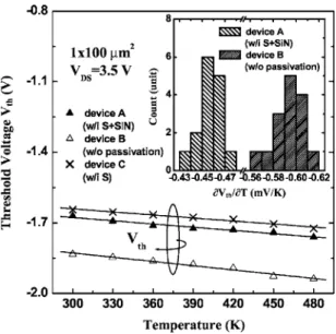
The threshold voltage共Vth兲 as a function of temperature is shown in Fig. 4. The biased voltage is fixed at VDS= 3.5 V. The inset shows the distribution of temperature variation rate in Vth, i.e., Vth/T, for devices A and B. The Vthis determined from the inter-cept point by the extrapolation of共IDS兲1/2vs V
GScurve. To obtain the required accuracy and validity, a statistical analysis concerning the variation of process uniformity is performed. There are more
Figure 1. The schematic illustrations of different passivations on the studied
HEMTs.
Figure 2. The gate-drain breakdown voltage共BVGD兲 and Schottky barrier
height共⌽B兲 as a function of temperature. The BVGDvalues are measured
than 15 samples in five times processes共process by process, device by device兲 used in this work. Due to the slight standard deviation of Vth/T in different samples, the moderate device characteristics are chosen for obtaining the reliable results. Along with the experimen-tal data, the Vthvalues of devices A, B, and C are decreased from −1.67, −1.83, and −1.64 to −1.76, −1.94, and −1.72 V as the tem-perature is increased from 300 to 480 K. Upon the sulfur passiva-tion, the lower density of interface traps presented between the drain-source and the gate edge would result in the increased⌽B.14 Hence, for devices A and C, the enhanced gate control ability and related lower Vth magnitudes are found. In particular, the Vth of device A is slightly degraded more than that of device C. This results from the hot carrier trapping in SiNx/AlGaAs interface, which leads to the additional leakage current and a negative shift of the Vth.10,11 Moreover, it is known that the device thermal stability is influenced by gate Schottky performance.4,7Due to the excellent Schottky be-haviors associated with high BVGD and ⌽B, the Vth/T, from 300 to 480 K, of devices A and C are −0.46 and
−0.428 mV/K, which are significantly better than that of device B 共−0.601 mV/K兲. This is certainly suitable for high-temperature ap-plications. As compared with device C, the slightly degraded tem-perature coefficient of device A is observed. This proves again that the lower thermal conductivity of SiNx layer may increase the de-vice operating temperature and lead to the relatively poorer rectify-ing performance of gate Schottky contact. Accordrectify-ingly, the rela-tively higher兩VGS兩 is needed to deplete the channel and then the Vth is little degenerated with the increase of temperature. Based on these results, it is known that the deviations of electrical properties and temperature coefficients between the devices A and C are negligible. Therefore, it is reasonable to conclude that the device with formal passivation shows the comparable dc characteristics to the device only with sulfur passivation.
Figure 5 illustrates the drain saturation current共IDS兲 and trans-conductance共gm兲 vs gate-source voltage 共VGS兲 of devices A and B at 300, 390, and 480 K. Obviously, by using the formal passivation, device A shows relatively better linear properties and high transcon-ductance with a wide operating regime between the temperature of 300–480 K. The transconductance performance of device A shifts toward more positive VGSregimes. This is caused by the improved gate Schottky characteristics in terms of enhanced gate control abil-ity. Also, to obtain advanced investigation and deeper understanding on the amplification performance, the output conductance共gds兲 is employed as17
gds=
冏
IDVDS
冏
VG=constant关3兴 From Eq. 3, the maximum transconductance共gm,max兲, gds, and IDS operating regime共IDS,op兲 of devices A and B as a function of tem-perature are shown in Fig. 6. The biased voltage is fixed at
VDS= 3.5 V. The IDS,opis defined as the IDSrange where the gm,max is larger than 90% of its peak value. The gm,maxof devices A and B are decreased from 236 and 215 to 207 and 179 mA/mm, respec-tively, as the temperature is increased from 300 to 480 K. The cor-responding gds are increased from 0.49 and 0.53 to 0.53 and 0.59 mS/mm, respectively. The widths of IDS,opare over 271共223兲 and 224共177兲 mA/mm for device A 共B兲 at 300 and 480 K. Appar-ently, the gm,maxand IDS,op共gds兲 values in the saturation region of device A are higher 共lower兲 than those of device B. This result demonstrates that the formal passivation is effective in eliminating the interface traps formation and suppressing the extrinsic共exposed gate region兲 and intrinsic 共below the gate兲 parts of leakage currents. In addition, the related temperature coefficients, i.e.,
Figure 3. Typical output current-voltage characteristics of devices A and B
at different temperatures.
Figure 4. The threshold voltage共Vth兲 as a function of temperature. The
biased voltage is fixed at VDS= 3.5 V. The distribution of temperature
varia-tion rate in Vth共Vth/T兲 for devices A and B is shown in the inset.
Figure 5. The drain saturation current共IDS兲 and transconductance 共gm兲 vs
gate-source voltage共VGS兲 of devices A and B at 300, 390, and 480 K. The
共gm,max/gm,max兲共1/T兲, 共gds/gds兲共1/T兲, and 共IDS,op/IDS,mo兲 ⫻共1/T兲, of device A 共B兲 are −6.46 ⫻ 10−4共−9.79 ⫻ 10−4兲, 3.31 ⫻ 10−4共5.88 ⫻ 10−4兲, and −9.81 ⫻ 10−4共−1.21 ⫻ 10−3兲/K, re-spectively, between the temperature of 300–480 K. This indicates that the gate control ability as well as the thermal stability of device A is improved under various temperatures. In other words, the de-graded amplification performance of device A is relatively insensi-tive to the increase of temperature. Thus, for the formal-passivated device, good properties of transconductance are achieved even if the temperature is elevated up to 480 K.
Figure 7 reveals the normalized drain saturation current共NIDS兲 and normalized threshold voltage共NVth兲 vs stress time. The related lifetime performance was examined by the accelerated stress condi-tions of VDS= 7.5 V and VGS= 0 V at 390 K. The biased condi-tions for IDS 共Vth兲 characterization are fixed at VDS= 3.5 V and VGS= −1.0 V共VDS= 3.5 V兲 at 390 K. As the stress time increases up to 429 h, the NIDSand NVthof device B共device C兲 drop 10.4 共7.9兲% and 5.9 共4.7兲% from its initial values, while these values are only 2.9 and 2.6% for device A. Evidently, with increasing the stress time, the degradations of electrical properties for device C are larger than those of device A. Although the devices A and C show the
comparable dc characteristics, the reliability performance of device C is often impeded by chemical instability of thinner sulfide layer against ambient atmosphere.9,19When the moisture or oxygen pen-etrates into the underlying AlGaAs surface, this results in the for-mation of native oxide and related G-R leakage currents. Thus, for device C, the enhanced sulfur-passivated AlGaAs surface eventually deteriorates back to its initial state. However, the reliability perfor-mance of device A is improved by employing an additional SiNx coating after sulfur passivation. This is because both the sulfur and SiNxpassivations could mitigate the interface traps, protect the sul-fide layer, and stabilize the surface improvement.10,11,14Therefore, the formal-passivated device exhibits relatively long-term electrical characteristics.
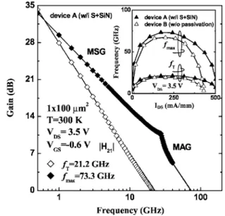
The microwave characteristics of device A at 300 K are depicted in Fig. 8. The inset shows unity current gain cutoff frequency共 fT兲 and maximum oscillation frequency共 fmax兲 vs drain saturation cur-rent共IDS兲 of devices A and B. The biased voltage is fixed at VDS = 3.5 V. For device A, the maximum fT and fmax are 21.2 and 73.3 GHz at 300 K. The corresponding maximum fT and fmax of device B are 19.2 and 67.1 GHz. Moreover, the studied devices A and B maintain 90% of their fT 共 fmax兲 peak values over large IDS operating regimes of 262 and 234 mA/mm at 300 K, respectively. Obviously, device A exhibits better characteristics in fT, fmax, and
IDS operating regime. Because the formal passivation allows the fabrication of high-quality metal/AlGaAs Schottky contact with low density of interface traps, this certainly reduces the channel output conductance and parasitic capacitance.7,20Consequently, the formal-passivated device with high-frequency operating capability and good linearity in microwave performance is obtained.
Conclusion
The temperature-dependent characteristics of HEMTs with sulfur and SiNxpassivations were studied and demonstrated. Experimen-tally, the formal-passivated device exhibits considerably enhanced device characteristics than nonpassivated device including higher gate-drain breakdown voltage 共39.3 V兲, higher Schottky barrier height 共0.993 eV兲, lower threshold voltage 共−1.67 V兲, higher maximum transconductance 共236 mS/mm兲, and lower output conductance 共0.49 mS/mm兲 at 300 K. The improved temperature coefficients on BVGD共−1.66 ⫻ 10−3/K兲, ⌽B共−3.23 ⫻ 10−4/K兲, Vth 共−0.46 mV/K兲, gm,max 共−6.46 ⫻ 10−4/K兲, and gds 共3.31
Figure 6. The maximum transconductance 共gm,max兲, output conductance
共gds兲, and IDSoperating regime共IDS,op兲 of devices A and B as a function of
temperature. The biased voltage is fixed at VDS= 3.5 V.
Figure 7. The stress time dependences on the normalized drain saturation
current共NIDS兲 and normalized threshold voltage 共NVth兲. The accelerated
stress conditions are VDS= 7.5 V and VGS= 0 V at 390 K.
Figure 8. The microwave characteristics of device A at 300 K. The unity
current gain cutoff frequency共 fT兲 and maximum oscillation frequency 共 fmax兲
vs drain saturation current共IDS兲 of devices A and B are shown in the inset.
⫻ 10−4/K兲 are also observed as the temperature is increased from 300 to 480 K. Besides, it is found that the studied device with for-mal passivations shows the comparable electrical properties and temperature coefficients to the device only with sulfur passivation. However, in contrast to the sulfur-passivated device, the degrada-tions of reliability performance on IDS 共2.9%兲 and Vth 共2.6%兲 are insignificant as the accelerated stress time increases up to 429 h. Therefore, the studied device provides the promise for high-performance and high-reliability electronic applications.
Acknowledgments
Part of this work was supported by the National Science Council of the Republic of China under contract no. NSC-95-2221-E-006-434-MY2. The authors are also grateful to National Nano Device Laboratories共NDL兲 for rf measurements.
National Cheng-Kung University assisted in meeting the publication costs of this article.
References
1. J. H. Tsai, IEEE Electron Device Lett., 23, 1共2003兲.
2. W. C. Hsu, D. H. Huang, Y. S. Lin, Y. J. Chen, J. C. Huang, and C. L. Wu, IEEE
Trans. Electron Devices, 53, 406共2006兲.
3. Y. S. Lin and Y. L. Hsieh, J. Electrochem. Soc., 153, G498共2006兲.
4. Y. Dong, X. M. Ding, X. Y. Hou, Y. Li, and X. B. Li, Appl. Phys. Lett., 77, 3839 共2000兲.
5. M. R. Ravi, A. DasGupta, and N. DasGupta, IEEE Trans. Electron Devices, 50, 532共2003兲.
6. S. W. Tan, H. R. Chen, W. T. Chen, M. K. Hsu, A. H. Lin, and W. S. Lour, IEEE
Trans. Electron Devices, 52, 204共2005兲.
7. P. H. Lai, C. W. Chen, C. I. Kao, S. I. Fu, Y. Y. Tsai, C. W. Hung, C. H. Yen, H. M. Chuang, S. Y. Cheng, and W. C. Liu, IEEE Trans. Electron Devices, 53, 1共2006兲. 8. D. J. Coleman, Jr., W. R. Wisseman, and D. W. Shaw, Appl. Phys. Lett., 24, 355
共1974兲.
9. Z. Chen, W. Kim, A. Salvador, S. N. Mohammad, O. Aktas, and H. Morkoc, J.
Appl. Phys., 78, 3920共1995兲.
10. Y. C. Chou, G. P. Li, D. Leung, Z. Y. Wang, Y. C. Chen, R. Lai, C. S. Wu, R. Kono, P. H. Liu, J. Scarpulla, and D. C. Streit, in Proceedings of 19th Annual IEEE GaAs
IC Symposium Digest, 165共1997兲.
11. A. Nagayama, S. Yamauchi, and T. Hariu, IEEE Trans. Electron Devices, 47, 517 共2000兲.
12. O. Wada, S. Yanagisawa, and H. Takanashi, Appl. Phys. Lett., 29, 263共1976兲. 13. P. H. Lai, S. I. Fu, Y. Y. Tsai, C. W. Hung, C. H. Yen, H. M. Chuang, and W. C.
Liu, J. Electrochem. Soc., 153, G632共2006兲.
14. H. Oigawa, J. Fan, Y. Nannichi, H. Sugahara, and M. Oshima, Jpn. J. Appl. Phys.,
Part 2, 30, L322共1991兲.
15. J. L. Wright, M. W. Marks, and K. D. Decker, in Proceedings of IEEE Seventh
Semi-Therm Symposium, 110共1991兲.
16. H. Ohno, H. Kawanishi, Y. Akagi, Y. Nakajima, and T. Hijikata, Jpn. J. Appl.
Phys., Part 1, 29, 2473共1990兲.
17. S. M. Sze, Semiconductor Devices: Physics and Technology, 2nd ed., Wiley, New York共1985兲.
18. K. E. Bohlin, J. Appl. Phys., 60, 1223共1986兲.
19. H. L. Chuang, M. S. Carpenter, M. R. Melloch, M. S. Lundstrom, E. Yablonovitch, and T. J. Gmitter, Appl. Phys. Lett., 57, 2113共1990兲.