The Effect of Inorganic/Organic Hybrid Quantum-Well Structure on Efficient White Organic Light Emitting Devices
Yu-Cheng Chen, Ming-Hua Wu, Po-Ching Kao*, Sheng-Yuan Chu
a)Department of Electrical Engineering, National Cheng Kung University, Tainan 70101, Taiwan
* Department of Electrophysics, National Chiayi University, Chiayi 60004, Taiwan
Keywords: OLED, Quantum-well structures
Phone: +886(6)275-7575 ext.62381 E-mail: [email protected]
ABSTRACT
In this study, the effect of MQW structures adopting inorganic material (sodium fluoride) has been demonstrated. Brightness, current efficiency was significantly enhanced with a NaF/NPB MQW structure being inserted. The admittance spectroscopy was measured to explain the different mechanism of reducing hole between organic/organic inorganic/organic MQW structures.
1. Introduction
Multilayer organic light-emitting devices (OLEDs) have attracted much attention because of their potential use in lightweight, fast-response full-color displays or lighting application ever since Tang and Van Slyke reported the first efficient OLED.[1] Besides, interest in application of white OLEDs (WOLEDs) technology for general solid-state lighting application or flat-panel display backlight has also been drastically increasing. Different structures have been fabricated to achieve white OLEDs with optimal EL properties and lots of effort had been put into improving the performance of WOLEDs and understanding their underlying mechanisms. In OLEDs, transport characteristics of carriers influence the zone (position) of excitons formed, the recombination processes and the electroluminescence properties of the device. Furthermore, the current efficiency and external quantum efficiency depend on the efficiency of carriers’
injection and on the balance between holes and electrons.[2] However, hole’s mobility is generally a few orders of magnitude higher than electron’s mobility in most organic materials.[3] Multiple-quantum-well (MQW) structures are widely acknowledged to be helpful in obtaining higher emission efficiency[4], reducing holes mobility[5-6] and confining excitons.[7-9] According to previous researches, some kinds of organic materials were adopted to form organic/organic multiple quantun-well(MQW) structure and obtained good results.[7-8] However, there is few study on adopting inorganic material to form inorganic/organic MQW structure for OLEDs and discussing the mechanism behind it.
2. Experimental
White emission layer were deposited in one single layer adopting single deposition source prepared by a solution mixing method. Predetermined amounts of the composing guest and host were first separately dissolved in toluene, followed by mixing together to obtain a solution with optimized weight ratio. The solution was then dried in oven prior to vapor deposition.
The evaporating current of blended source remains almost same with pure host source. The ITO (indium tin oxide) coated glass substrate (Merck Display Technology) with a film thickness of 2 m a nd a s he e t resistance of approximately 15 Ω/square was cleaned sequentially with mixture of neutraler reiniger and de-ionized water (1:3 volume), de-ionized water, isopropanol and ethanol, followed by UV-ozone treatment (Jetlight UVO-42) for 20 min. The hole injection layer CuPc, the hole transport layer NPB, blue-emitting material (MADN), orange doped dye rubrene, electron transport and hole-blocking layer TPBi, electron injection layer LiF and aluminum cathode were subsequently deposited to obtain the fluorescent
white-emitting OLEDs devices [ITO/CuPc/NPB/NPB/( NaF)n /MADN:rubrene /TPBi
/LiF/Al] (Figure 1 (c)). The thickness of each layer was controlled by a calibrated quartz crystal oscillator equipped within the deposition chamber. The deposition rate was 0.1 Å/s for inorganic layer, about 1-2 Å/s for the organic layer and 4-5 Å/s for the aluminum metal cathode. The active area of the devices was 6.25 mm2 (2.5 mm × 2.5 mm). And n is number varied from 1 to 2.
ITO/C60/(NPB/C545T or NaF)n/NPB/MoO3/Al is hole only device structure. Admittance spectroscopy of devices with structure ITO/NPB、NaF、C545T/Al is performed to discuss the electrical behavior of MQW structure by using Agilent 4294A network analyzer with an oscillation level of 0.1v.
The current density-voltage (J-V), luminance-voltage (L-V) characteristics and CIE chromaticity coordinate were measured with a source meter (Keithely-2400) combined with a luminance meter (Photo Research PR650). The ultraviolet visible (UV-Vis) absorption spectra were measured with a Hitachi U3310 UV-Vis spectrophotometer. The HOMO energy-levels of the
organic materials were measured in high vacuum using UPS (ultraviolet photoelectron spectroscopy) conducted with He I (21.2eV) discharge lamp. The corresponding lowest unoccupied molecular orbital (LUMO) energy levels were calculated by LUMO = HOMO - Eg using their HOMO energy levels and optical band gaps (Egs), which in turn were estimated from the lowest-energy absorption edge (λabs) of their absorption spectra (Eg = 1240/λabs). All the measurements were performed in ambient conditions.
3. Results and discussion
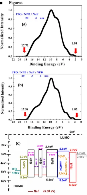
In order to make sure the deposition of chosen inorganic material on holes transport material NPB could form the MQW structures we expect. UPS measurement was performed to identify the HOMO level of NPB deposited by 3 nm NaF. Figure 1 (a) and (b) show the UPS spectra for electron cutoff region and the highest occupied molecular orbital (HOMO) region of ITO/NPB/NaF and ITO/NPB/NaF/NPB, respectively. The HOMO level of pure NPB locates at about 5.5 eV based on our previous research.[11] According to elucidation of other published works, the HOMO level can be calculated as 5.33 eV and 5.51 eV ,respectively. And according to it, Figure 1 (c) could be plotted.
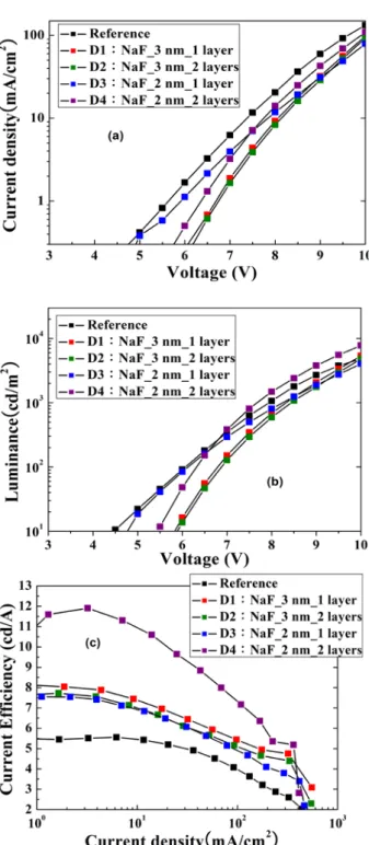
Figure 2 (a) shows the current density-voltage characteristics of white OLEDs with various numbers NaF well (2 nm and 3 nm), and luminance-voltage characteristic is shown in Figure 2 (b). For the purpose of clarity, representative and optimized thickness (2 nm and 3 nm) of NaF is chosen to show the effect after MQW structure being inserted.Clearly, the current density of the devices decreases gradually with an increase in well numbers. The turn-on voltage (the bias required to produce measureable luminance of 10 cd/m2
Then the holes only devices were fabricated to prove and discuss the effect of inorganic/organic MQW structure.
The Figure 3 shows the log-log plot of the J-V characteristics for holes only devices with various MQW structures (the results of MQW formed by C545T come from our previous work). The hole-only device with NaF shows very special electrical behavior, the slope of J-V curve changes with the increase of applying voltage.
According to the slope of J-V curve, it operates not as pure organic materials in space-charge-limited-current (SCLC) region from low to high applying voltage. It shows the behavior like resonant tunneling effect and it will be discussed later. From our previous work, NaF and C545T have similar work function. It is noteworthy why they performed differently and C-F spectra were measured to elucidate the effect and mechanism. Figure 4 shows 300 K capacitance-frequency(C-F) spectra, it shows that NaF owns capacitance about one order higher than organic materials NPB and C545T at low frequency. Inset is of the photo how the measurement of admittance spectroscopy was performed. According to previous researches [9-10], it will affect the equivalent circuit of the WOLEDs when NaF inserted. Furthermore, MQW with NaF has higher capacitance and it could not only reduce the holes mobility but also causes the resonant tunneling effect as our previous research demonstrated [11]. There have been many reports about the resonant tunneling effect originating from the quantum well structure that have revealed negative differential resistance (NDR) in devices. Resonant tunneling occurs when the energy of the quasi-bound state of the quantum well matches that of an incident charge.[12] Space charge starts to accumulate in the quantum well of NaF with increasing applied voltage at the starting region, corresponding to range from 4 V to 6 V. The accumulation of charges soon reaches a maximum in which the bound state of NaF quantum well owns the same level at the edge of organic material NPB.
This corresponds to the range of 6 V to 10 V. After 10 V, the current is contributed by the tunneling of accumulated charges of the quantum well to unoccupied NPB collector. However, the low frequency capacitance of C545T and NPB is almost the same. MQW consists of pure organic materials will not change the capacitance of equivalent circuit of the device and shows no effect on the electric behavior of the holes transport. As discussion, inorganic/organic MQW indeed exist different mechanism on manipulating carrier transport.
) increases from 4.5 V (reference device) to 4.7 V for the devices with 1 layer of 2 nm NaF and drastically to 5.5 V for 2 layers.
The current density decrease and turn-on voltage increase are direct outcome of the MQW structures formed. Current density was decreasing with the number and thickness of NaF/NPB quantum well unit increasing. Simultaneously, luminance remains almost the same with only a little increase in turn-on voltage. The optimal number was two units (2 nm). With the optimal structure, OLED could reach high current efficiency of 12 cd/A which is obviously superior to 5.5cd/A for the reference device. It could be contributed to the good amount balance between holes and electrons.
Conclusion
We demonstrated the effect of inorganic/organic of MQW structure inserted in white OLEDs (ITO/CuPC/NPB/MADN:rubrene/TPBi/LiF/Al). The MQW structures formed by 2 nm NaF (1 layer) reduced hole mobility in NPB nearly to match with the electron mobility of TPBi that achieved a better hole-electron balance. A maximum efficiency of 12 cd/A was obtained, which is 118% higher than that of reference device (5.5 cd/A), which remained even after the roll-off effect caused by high current density. The hole-only devices show the different electric behaviors between organic/organic and inorganic/organic MQW. The admittance spectroscopy was measured to explain the different mechanism and effect of reducing hole between
organic/organic and inorganic/organic MQW structures.
The results demonstrate with proper inorganic materials consisting of optimal MQW structure, it could lower the mobility of hole-transporting layer and reducing the amount of holes to optimum value and increases the devices performance, making it applicable for the fabrication of efficient fluorescent white OLEDs.
References
[1] C. Tang, et al., "Electroluminescence of doped organic thin films," Journal of Applied Physics, vol. 65, pp. 3610-3616, 1989.
[2] S. Zhan, et al., "A novel hole-blocking layer NaF between the α-naphthylphenyliphenyl diamine and ITO," Applied Surface Science, vol. 253, pp.
4374-4376, 2007.
[3] C. F. Qiu, et al., "Room-temperature ultraviolet emission from an organic light-emitting diode,"
Applied Physics Letters, vol. 79, pp. 2276-2278, 2001.
[4] J. Huang, K. Yang, Z. Xie, B. Chen, H. Jiang, and S. Liu, "Effect of well number on organic multiple-quantum-well electroluminescent device characteristics," Applied Physics Letters, vol. 73, pp. 3348-3350, 1998.
[5] Y. Qiu, Y. Gao, L. Wang, P. Wei, L. Duan, D.
Zhang, and G. Dong, "High-efficiency organic light-emitting diodes with tunable light emission by using aromatic diamine/5, 6, 11, 12-tetraphenylnaphthacene multiple quantum wells," Applied Physics Letters, vol. 81, p. 3540, 2002.
[6] Y. Qiu, Y. Gao, P. Wei, and L. Wang, "Organic light-emitting diodes with improved hole-electron balance by using copper phthalocyanine/aromatic diamine multiple quantum wells," Applied Physics Letters, vol. 80, p. 2628, 2002.
[7] T. J. Park, W. S. Jeon, J. W. Choi, R. Pode, J.
Jang, and J. H. Kwon, "Efficient multiple triplet quantum well structures in organic light-emitting devices," Applied Physics Letters, vol. 95, pp.
103303-3, 2009.
[8] S.-H. Yang, B.-C. Hong, and S.-F. Huang,
"Luminescence enhancement and emission color adjustment of white organic light-emitting diodes with quantum-well-like structures," Journal of Applied Physics, vol. 105, pp. 113105-7, 2009.
[9] M.-H. Ho, et al., "Study of efficient and stable organic light-emitting diodes with
2-methyl-9,10-di(2-naphthyl)anthracene as hole-transport material by admittance
spectroscopy," Applied Physics Letters, vol. 94, pp. 023306-3, 2009.
[10] M.-T. Hsieh, et al., "Study of hole concentration of 1,4-bis[N-(1-naphthyl)-N[sup
[prime]]-phenylamino]-4,4[sup [prime]] diamine doped with tungsten oxide by admittance spectroscopy," Applied Physics Letters, vol. 89, pp.
103510-3, 2006.
[11] Y.-C Chen, et al.,”Investigation of Time-Dependent UV-Ozone Treatment on an Ultra-Thin AgF Buffer Layer for Organic Light-Emitting Diodes,” Journal
of The Electrochemical Society, vol. 159, pp.
H388-H392, 2012.
[12] T. J. Foster, M. L. Leadbeater, L. Eaves, M.
Henini, O. H. Hughes, C. A. Payling, F. W.
Sheard, P. E. Simmonds, G. A. Toombs, G. Hill, and M. A. Pate, "Current bistability in double-barrier resonant-tunneling devices,"
Physical Review B, vol. 39, pp. 6205-6207, 1989.
■ Figures
Fig. 1 UPS spectra of (a) ITO/NPB/NaF (b) ITO/NPB/NaF/NPB (c) Schematic diagram of MQW structure, device structure and energy level for NaF
(a)
(b)
(c)
Fig. 2 (a) J-V (b)L-V (c)Yield-Current Density characteristics of white OLEDs with various NaF/NPB MQW structure.
Fig. 3 The J-V characteristics of hole-only devices with various MQW structure
Fig. 4 Spectra of the admittance spectroscopy, measured on a device with an ITO/Various materials (70 nm)/Al structure. Inset is of the photo how the measurement of admittance spectroscopy was performed.