A 15mW 69dB 2Gsamples/s CMOS Analog
Front-End for Low-Band UWB Applications
Hua-Chin Lee, Chien-Chih Lin, Chia-Hsin Wu, Shen-Iuan Liu, Chorng-Kuang Wang and Hen-Wai TsaoGraduate Institute of Electronics Engineering and Department of Electrical Engineering, National Taiwan University, Taipei, Taiwan 10617
{huachin, tmt}@ aic.ee.ntu.edu.tw, r88066@ ee.ntu.edu.tw, {lsi, ckwang, tsaohw}@ cc.ee.ntu.edu.tw
Abstract—This paper presents a CMOS analog front-end (AFE)
for short range impulse radio system in low-band ultra-wideband (UWB) based on 2ns width PAM modulation. The wideband amplifier provides 69dB gain from 30MHz to 1.2GHz, realized by a limiting amplifier with an active-inductor load and a cross-coupled gm gain-boosting cell in each gain stage. The received signal is digitized at 2GHz sampling rate by the 8 parallel 1-bit ADCs, each of which is composed of transmission-gate type sample-and-hold circuits and a dynamic differential comparator. A timing generator based on a 4-stage ring oscillator in a PLL is employed to provide 8-phase 250MHz clocks. Realized in 0.18μm CMOS technology, the AFE occupies a 1.0 x 1.2 mm2 active area with the 3rd order loop filter integrated in the same die. This chip also includes an integrated pulse generator for loop-back self-testing purpose. The receiver AFE achieves 200μV sensitivity and consumes 15mW from a 1.8V supply.
I. INTRODUCTION
In recent years, the short-range impulse radio UWB below 960MHz has raised interests in the applications of radio frequency identification (RFID), localizer and sensor networks [1]. By using repetitive pulses, it transmits signals over a much wider frequency band than conventional carrier-based radio systems. The UWB system features in immunity to multi-path fading, potentially unlicensed operation due to the low spectral power density, security against eavesdropping, and penetrating through obstacles. Based on its application, the development of the impulse radio transceiver should target on low power consumption, low hardware complexity and low cost.
Due to the carrier-less property, power-consuming circuits, such as up/down conversion and IF filters, can be eliminated. The receiver is required to distinguish the digital data by correlating the pulses after adequate amplification. The correlation can be performed in the analog domain or the digital domain. The former requires timing signals with fine resolution and high performance mixer with integration and dump circuits. The latter digitizes the received signals and uses the digital circuits to conduct the correlation. This design is based on the digital correlation approach for its
robustness in the pulse search procedure. The analog front-end complying with the digital backfront-end is designed to achieve simple hardware complexity and low power consumption.
This paper presents an analog front-end (AFE) architecture and the circuit designs for the low band impulse radio UWB. Section II introduces the designed signals and circuit specification. The circuit architecture is described in section III. In section IV, the simulation results are presented. Finally, section V draws the conclusion.
II. SIGNALING AND SYSTEM SPECIFICATIONS
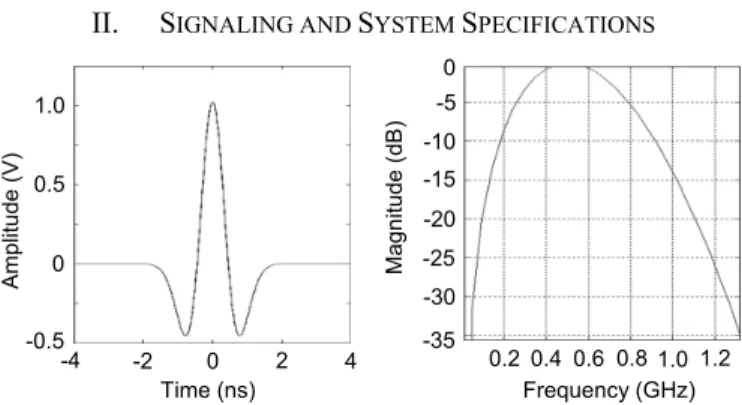
Fig. 1 The received pulse and its spectrum
This impulse radio system adopts binary pulse amplitude modulation (PAM) with 2ns width pulses for the signal band from 30MHz to 960MHz. After the differentiation effects caused by the antenna, the received pulse is modeled by a 2nd derivative Gaussian pulse shape [2] derived in (1). The time domain shape and spectrum are shown in Fig. 1. The received signals are then sampled at 2Gsamples/s for pulse correlation and data detection. The pulse repetition time is another issue to design the signaling. Short pulse repetition time increases the data rate, but has severe interference problems. On the contrary, long pulse repetition time provides better immunity while lowering the data rate. Based on the channel property, the RMS delay is 10~20ns [3]. In this work, the pulse repetition time is designed to be 16ns. M ag n itu de ( dB ) 0 -5 -10 -15 -20 -25 -30 -35 Frequency (GHz) 0.2 0.4 0.6 0.8 1.0 1.2 A m pl itu de ( V ) 0 -0.5 0.5 1.0 Time (ns) 0 -2 2 4 -4
This work is supported by MediaTek Inc., HsinChu, Taiwan
368 0-7803-8834-8/05/$20.00 ©2005 IEEE.
2 ) / ( 2 2] ) ( 4 1 [ ) ( t Td d e T t A t p = - -p
The pulse train is further spread by a Golay spreading code [4]. It provides identification for different users, and smoothes the spikes of the spectrum. The longer the spreading code is, the better immunity to interferences and noises the system has. However, it reduces the data rate since it uses multiples of pulses to send one bit of data. Based on different channel conditions, the length of spreading code is designed from 0 to 1024, and the corresponding data rate is 62.4Mbps to 61kbps, respectively.
For the required transmitted power should be less than -41.3dBm/MHz regulated by FCC, the emitted pulses have the power of -17dBm over the effective bandwidth of 500MHz. According to the indoor channel analyzed by USC [3], the maximum path loss in 10 meters is 64dB. Considering the implementation loss of 10dB, the desired total gain of the receiver is 74dB. With the gain of the LNA is 10dB, the gain of the succeeding font-end circuits in the receiver should be above 64dB. .
III. ANALOG FRONT-END ARCHITECTURE
. . . . . . R E S Y N C H R O N IZ E D B U F F E R . . .
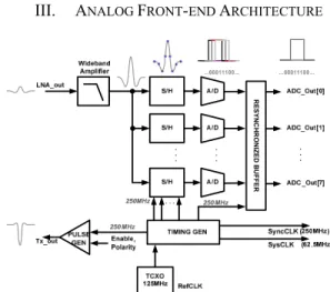
Fig. 2 Analog front-end architecture
The reception of the impulse radio signals requires high speed sampling with precise timing for the correlation procedure. Fig. 2 shows the proposed analog front-end circuit architecture that contains a wideband amplifier, 8-channel parallel 1-bit ADCs and resynchronization buffer clocked by a built-in timing generator. The amplifier provides 64dB gain so that the output voltage fits in the detectable range for the ADCs in the 10-meter transmission range. The minimum input of the wideband amplifier is 200uV, and the minimum input of the ADCs is 100mV considering the output offset of the amplifier. The resynchronization buffer resynchronizes the 8-phase consecutive outputs from the ADCs to facilitate the digital baseband to detect the impulse and decode the data. The timing generator provides precise timing signals for ADCs at the 2Gsamples/s sampling rate and with 100ps jitter tolerance [1]. It utilizes the 4-stage ring oscillator in a PLL loop to generate 8 phases of 250MHz clocks with an external
125MHz TCXO reference. In addition to the receiving path, a simple pulse generator is implemented for self-test purpose to generate 2ns wide pulses based on the on-chip timing signals. The circuit design of each block is detailed as follows.
A. Wideband Amplifier
The wideband amplifier is configured as a limiting amplifier as shown in Fig. 3. It consists of four gain stages providing a total gain of 69 dB and a buffer stage driving the parallel ADCs that appear as about 4pF load. Due to the high voltage gain, the circuit is sensitive to offsets and thus DC offset cancellation network is added in the negative feedback path. The extraction network is a low-pass filter using on-chip MOS resistors and MOS capacitors with the cut-off frequency at 30MHz. The resulting amplifier loop has the 30MHz to 1.2GHz bandpass characteristics.
Fig.3 Wideband amplifier with offset cancellation Each gain cell, shown in Fig. 4(a), employs a differential pair to provide high gain and broad bandwidth. The active inductor is used as the load to cancel the output pole and enhance its frequency response [5]. Cross-coupled NMOS transistors are put at the output nodes to provide high output impedances and increase the voltage gain. The first gain stage has another input from the offset extraction feedback and demands a subtraction function to remove the effect. Shown in Fig. 4(b), it resembles the gain stages except the cross-coupled devices are replaced by the negative offset feeding ones.
Fig. 4 (a) Gain stage circuit (b) Offset subtractor
B. ADC
The 1-bit ADC contains a sample-and-hold circuit and a differential comparator, shown in Fig. 5(a) and 5(b) respectively. The sample-and-hold circuit employs the transmission gate to reduce the input impedance variation
(a) (b)
(1)
during the on/off states. The dummy switch is added after the transmission gate and the hold capacitor to eliminate the clock-feed-through effect.
Fig. 5 (a) Sample-and-Hold Circuit (b) Differential comparator
Fully differential circuitry is used to have better power noise rejection and immunity to common mode noises. Differential comparator is employed as in Fig. 5(b) with auxiliary transistors M9a and M10a that help to pre-charge and pre-discharge the output latches and speed up the response. It results in 0.2ns rise time and 0.3ns fall time in state transition. However, device mismatches in the differential circuits brings about the comparator offset. From Fig. 5(b), by setting transistors channel width W2=W4=WA and W1=W3=WB, the input voltage that changes the comparator state is [6][7]
) ( + -+- = ref -ref W W sh sh A B
By varying WA and WB, the threshold of the comparator can be adjusted to the desired level. Equation (2) implies that the offset of the comparator depends on the mismatches among M1-M4 when M5-M12 are assumed to match perfectly.
Furthermore, the total offset voltage consists of the sum of the offsets in both source coupled pairs. The offset voltage of one differential pair can be derived as [6]
) ( 2 b b D + D -+ D = L L T gs T OS R R V V V V
where ΔVT, ΔRL and Δβ are the mismatches of threshold voltage, load resistance and transistor dimension respectively. VT, RL and β are their average values. The offset voltage in this comparator architecture is dominated by Δβ, which suggests that the lower the Vgs, the smaller the offset [6].
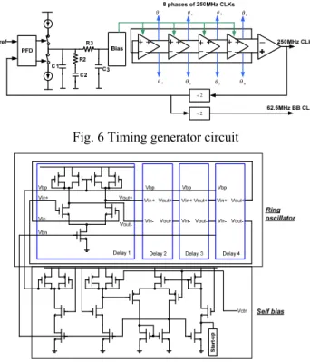
C. Timing Generator
Fig. 6 shows the architecture of the timing generator. The ring oscillator VCO is composed of 4 delay stages to provide 8 phases clocks at 250MHz for the ADCs. A third order loop filter is integrated in the chip with MIM capacitors and Poly resistors to set the loop bandwidth to
5MHz. The delay stage is a differential pair with the
symmetric load [8] controlled by the self-biased circuitry, as depicted in Fig. 7. The bias voltage of the NMOS current source is continuously adjusted in order to provide a bias current independent of supply and substrate voltages. The self-bias network takes advantage of the replica of the delay cells and generates the proper biasing voltages for the PMOS loads and the NMOS tail current devices from the control voltage generated by the loop filter.
2 ¸ 1 q q2 q3 q4 5 q q6 q7 q8 2 ¸
Fig. 6 Timing generator circuit
Fig.7 VCO and self-bias circuits IV. SIMULATION RESULTS
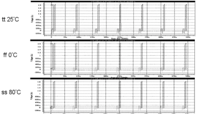
The front-end circuits for UWB are designed using 0.18μm CMOS technology. The receiving blocks have been integrated and simulated using SpectreRF. Fig. 8 shows the post-layout simulation results of the wideband amplifier frequency response. The gain achieves 69dB for the bandwidth from 30MHz to 1.2GHz. Besides, it has linear phase response in the band of interest. Fig. 9 shows the post-layout simulation results of the 1-bit ADC with the input threshold of 100mV. When the input pulse is amplified to above 100mV, the ADC acquires the correct data and outputs the digital signals in 1 bit. Under different process corners and temperature conditions, the 1-bit ADCs can operate correctly to digitize the input pulses. Fig. 10 shows the 8 phases of 250MHz clocks from the designed timing generator. For different process corners from the foundry models, the timing signals provide stable and precise timing information. The total power consumption for the whole chip is 15mW with 1.8V power supply. Shown in Fig. 11, the chip occupies 1.0 x 1.2 mm2 active area. The performance of this chip is summarized in Table 1.
(a) (b)
(2)
(3)
Fig. 8 The amplitude and phase responses of the amplifier
Fig. 9 Post-layout simulation of 1-bit ADC
Fig. 10 Post-layout simulation results of timing generator Table 1 Performance summary of UWB AFE
Design Technology 0.18um CMOS 1P6M
Chip core area 1.0 x 1.2 mm2
Power consumption 15mW
Receiver sensitivity 200uV (minimum)
Gain of receiver chain 69dB
AFE bandwidth 30MHz-1.2GHz
AFE sampling rate 2Gsamples/s
ADC resolution 8-phase parallel 1 bit
Internal clock rate 8-phase 250MHz
Clock jitter 100ps
Fig. 11 Layout of low-band UWB AFE V. CONCLUSION
A single chip receiver analog front-end is designed for the impulse radio UWB system. For the low-band UWB operation, the pulse generator generates 2ns width PAM pulses in 16ns pulse repetition time. The AFE provides 69dB gain with a limiting amplifier that achieves high gain and wide bandwidth by using an active-inductor load and a cross-coupled gm gain-boosting stage. It produces 1-bit digital signals at 2GHz sampling rate for digital correlation by 8 parallel ADCs clocked by a timing generator with 8 phases of 250MHz clocks. Implemented in 0.18μm CMOS technology, the chip integrates all the front-end circuits and consumes 15mW from a 1.8V supply.
ACKNOWLEDGMENT
The authors would like to thank Prof. Tzi-Dar Chiueh, Mr. Chun-Pang Wu and Mr. Chia-Hsiang Yang for helpful discussion on the system. They would also like to thank MediaTek Inc. for the support, and Chip Implementation Center (CIC) for the chip implementation.
REFERENCES
[1] Ian D.O., Mike SW Chen, Stanley BT Wang, Robert W. Brodersen, "An Integrated, Low Power, Ultra-Wideband Transceiver Architecture for Low-Rate, Indoor Wireless Systems", IEEE CAS Workshop on Wireless Communications and Networking, Sept. 5-6, 2002
[2] M. Z. Win and R. A. Scholtz, “Impulse radio: how it works,” IEEE Commun. Lett., vol. 2, no. 2, pp. 36 –38, Feb 1998.
[3] D. Cassioli, M.Z. Win and A.F. Molisch, “The Ultra-Wide Bandwidth Indoor Channel: From Statistical Model to Simulations”, IEEE Journal on Selected Areas in Communications, Vol.20, No.6, pp.1247-1257, Aug. 2002
[4] Chia-Hsiang Yang, Yu-Hsuan Lin, Shih-Chun Lin, Tzi-Dar Chiueh, “Design of a low-complexity receiver for impulse-radio ultra-wideband communication systems”, IEEE Internation Symposium on Circuits and Systems, pp.125-128, 2004
[5] Eduard Sackinger and Wilhelm C.Fischer,”A 3-GHz 32-db CMOS limiting amplifier for Sonet OC-48 Receiver” IEEE JSSC , vol. 35, No. 12, Dec. 2000.
[6] L. Sumanen, M. Waltari, K. Halonen, “A Mismatch Insensitive CMOS Dynamic Comparator for Pipeline A/D Converters”, IEEE ICECS 2000
[7] TB Cho, PR Gray, “A 10b, 20Msamples/s, 35mW Pipeline A/D Converter”, IEEE JSSC, Vol. SC30, No. 5, March 1995
[8] J.G. Maneatis, M.A. Horowitz, “Precise Delay Generation using Coupled Oscillators”, IEEE Journal of Solid-State Circuits, Volume 28 , Issue 12 , pp1273-1282, Dec. 1993 Amplitude response (dB) Phase response (deg) 371