Design of System Resource Manager of Reconfigurable Architecture
Chih-Tung Lin
Shi-Jinn Horng
Chao-Jang Hwang
Yi-Shu Hung
National Taiwan
University of Science
and Technology
National Taiwan
University of Science
and Technology
Yuan Ze
University
Yuan Ze
University
jdung23@yahoo.
com.tw
horngsj@yahoo.
com.tw
cschwang@saturn.
yzu.edu.tw
drung0418@gmail.
com
Abstract-
This paper is mainly to propose a resource manager for the dynamic reconfigurable computing architecture. In order to make the system to replace the module accurately, the resource manager must thoroughly possess resource indices to present current status of hardware. By these resource indices, the system determines whether the module is reconfigurable or not. We evaluate the system resource by retrieving, monitoring, and supervising. The system can be effectively cut apart based on the complexity of the application program. The system can be implemented by hardware to increase and accelerate the efficiency of operation.Keywords: reconfigurable architecture, system resource manager, resource index.
1. Introduction
Nowadays, reconfigurable architecture can be applied in many applications, for instance, Digital Signal Processing (DSP), Finite Impulse Response Filter (FIR), and Fast Fourier Transform (FFT). On the one hand, it provides the flexibility that Application Specific Integrated Circuit (ASIC) lacks. On the other hand, it can increase the system performance and decrease the developing cost. If hardware resource information of reconfigurable architecture cannot be handled well, it cannot be manipulated extensively.
In the traditional computer architecture, the processing is mainly executed by CPU; the system can be applied to different applications by different software. In order to increase the efficiency of system processing, we can use co-processor. Because many different functions are to be processed, we need different co-processor to execute the functions. How to support the flexibility of co-processor in system, reconfigurable architecture can configure different
co-processors according to different functions in the system [1].
Simultaneously, the system can be configured into different architectures according to distinct specification. For example, Broadband wireless communication, it may need different bandwidth which can be dynamically configured into different hardware. In the same way, the digital filter may need to dynamically configure different hardware for different pass band frequency of the signal. Reconfigurable architecture possesses the function unit more flexibly and efficiently.
Before the system being reconfigured, we need to consider the status of hardware resource. But how to manage hardware resource effectively is an important thing, so we propose a system resource manager (SRM) to manage hardware resource.
In this paper, we define SRM mechanism to determine whether the system can be configurable or not.
Figure 1. Flexibility and Performance Figure 1. shows the clear illustration of the efficiency in reconfigurable architecture.[2] It can obviously be seen that the efficiency is nearly fit in with the circuit of ASIC while using reconfigurable hardware. Moreover, with extreme flexibility, reconfigurable architecture can make hardware possess a wide variety of functions to enhance the flexibility of hardware. When current circuit is
limited, it can take reconfigurable architecture as a means to make the circuit possess distinct functions; meanwhile, the efficiency can massively exceed the function of instruction set.
2. Resource Manager
2.1. Background Statement
As reconfigurable architecture utilizes the logic element of FPGA, we must understand the current situation of FPGA. The resource manager can control the reconfiguration or replace the module’s function. The resource information of the system can be captured, monitored and supervised to offer the system as a reference. Thus we build a resource manager for the system to manage the system resource.
2.2. Resource Manager Information
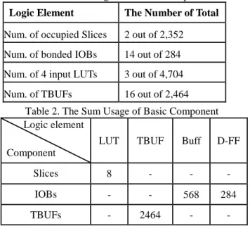
According to the current situation of FPGA, it can be divided into four kinds of components: Slice, IOB (Input/ Output Block), LUT (Look Up Table), and TBUF (Tri-state Buffer). In general, we can check the situation of these four elements to form a basis for the Logic Gate and to take the used count as resource information. After the resource information is interpreted by the system resource manager, we can exactly and clearly understand the current situation of FPGA. Basically, the component of Slice is mainly composed of two LUT elements. As for IOB, it generally includes three D Type Flip-Flops, one Input Buffer, one Output Buffer, and one Tri-state Buffer.
In order to be more familiar with FPGA, resource information can specifically be subdivided into LUT, Tri-state Buffer, Register and D Type Flip-Flop. These components can be represented as for resource index. This resource information can represent current used count of logic gate. From Table 1, we can recognize the maximum used count for each component, and the correlation between these components and the sum of logic gate can be referred to Table 2.The first row of Table 2 shows the basic logic element and the first column indicates the different kinds of components of FPGA. Due to each Slice is composed of two LUT elements, its sum of usage seems to be seen a half of amount in LUT. In Table 1, three LUT are used; relatively, it can be regarded as one and half usages in Slice, and two slices are used in this table. Hence, as we can see,
analyzing the utility rate of basic logic element can merely take down the utility rate of LUT.
Table 1. The Usage of Module Component
Logic Element The Number of Total
Num. of occupied Slices 2 out of 2,352 Num. of bonded IOBs 14 out of 284 Num. of 4 input LUTs 3 out of 4,704 Num. of TBUFs 16 out of 2,464
Table 2. The Sum Usage of Basic Component Logic element
Component
LUT TBUF Buff D-FF
Slices 8 - -
-IOBs - - 568 284
TBUFs - 2464 -
-2.3. The Design of Resource Index Access
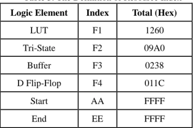
Each data has 24 bits, first 8 bits stand for current locations that can be used to differentiate initiation and the place of each basic component and the rest of 16 bits indicate current logic element counts of usage.Each group of resource information includes six groups of basic logic components; at the same time, we also define AA and EE as the beginning and the end indexes to represent the initiation of the data. If there is no resource being used in the recording column, it can be administered 16 Bits (FFFF) to express this column has no resource be utilized. As a result, each group of information is totally composed of six sets data; four sets of information indicate basic logic components, and two sets of information present the initial and the terminal. Among each set of information, the column of using count is 16 Bits and the information section is 8 bits; each set of information will need 24 Bits. For each sub module, the resource information will take 144 Bits. Eventually, the sum of usage in each set of resource information will represent with Hexadecimal as Table 3.
Table 3. The Definition of Resource Index
Logic Element Index Total (Hex)
LUT F1 1260 Tri-State F2 09A0 Buffer F3 0238 D Flip-Flop F4 011C Start AA FFFF End EE FFFF
2.4. The Capturing Architecture of System
Resource Information
With the establishment of resource index and the location of information, we need to take great action to put resource index and sub module separately. The main purpose is to decrease the using space in sub module based on the working performance of sub module. Thus, we get further to subdivide the reconfigurable architecture from the primary and then take sub module from the reconfigurable district to extra add the segment code for representing sub module sector. Meanwhile, this situation we are so-called Sub Module Segment Value (Sub-SV). In addition, we try to reduce the bits of segment code in order to cut down the application of sub module’s space. Based on the reason above, we use three bits to express sub module sector and they can represent eight different groups of sub module in the intact system. Figure 2 is the architecture of sub module.
Figure 2. Sub Module Architecture As for the portion of the fixed module, we modify the prime reconfigurable architecture and also add three parts into this system: Memory Unit, Control Unit and UART. Memory Unit is the storage agent for RAM, which store sub module in resource information. Next, Control Core is mainly responsible for four kinds of situations, including receiving request signal from the system, receiving transmitting segment code from sub module, reading the resource information of current stage of sub
module from Memory Unit, and installing Buffer in UART and being conveyed by UART after receiving information. Then, UART conveys the resource information from Buffer to the system. Figure 3 is the specific architecture of the whole fixed module.
Figure 3. Fixed Module Architecture In the unit of Control Core, the sequence of control is based on Finite State Machine (FSM) as Figure 4 ; it is mainly in charge of transmitting and receiving the signal in all unit of the fixed module. Control Core is required to execute signal receiving from the segment code, convey memory address, get resource information from Memory Unit and transmit register value to UART. In order to do the work accurately above, we attempt to produce the following regulations to collocate the execution of Finite State Machine and achieve the expected goal.
If the system wants to get usage information of FPGA which have reconfigured, it needs to send a request signal first. After the control core receives a request signal, it will send a request signal to sub module for getting current Sub-SV reconfigured.
When the sub module receives a request signal, it will send current Sub-SV to control core back. Then the control core receives the signal from sub module, it will call the case number buffer to send case 1 signal. After the case 1 is sent, the control core executes select case.
Case 1: Count the value of start address in memory. Resource index include six basic components usage data and each sub module resource index has its own address. Address counter has to count each start address, and send it to memory for getting correct address. After finishing count of start address, the address counter will send a signal to case number buffer proceeding next case.
Case 2: After getting start address, the receive counter will store and integrate resource index data into buffer. Then send complete signal to case number buffer proceeding next case.
Case3: When the control core finished case1and case2, it will send resource index data through UART to system.
Each case includes its own repeated state, so we adopt select case model design to execute each case. When the current case is finished, the next case would be executed.
The control core finishes the above three case, it would not execute case until the next request signal coming.
Figure 4. Finite State Machine
2.5. The Unit of System Resource Manager
Before the system starts to run the application program, we need to consider the priority of utilize hardware (FPGA) or software (general purpose processor) to do execution. When the system determines using hardware to run the program via algorithm, System Resource Manager (SRM) will make diagnosis of hardware resource index. From these hardware resource indexes, we can recognize that whether hardware resource is enough or not. If hardware resource is enough to execute the program, SRM can configure a function unit. However, if hardware resource is not sufficient, the application will be executed by software. The operational function work can refer to figure 5.
3. System Implementation
3.1. System Architecture
Due to the ordinary application program is mainly administrated by general purpose processor, if some complicated algorithm being partitioned and
switched to hardware (FPGA) executing. The efficiency of the whole system can be enhanced [3][4][5]. In order to advance the executive efficiency of the whole system, we design some rules to determine whether the work is done by hardware or software .The whole system architecture is shown in figure 6.
If the system to execute the application program, it gives MicroBlaze[6][7][8] to implement the whole application source code; the system resource manager (SRM) gauge whether the segment should be separated from the complicated application program. If the segment is separated, it will be implemented by reconfigurable module. Based on the current situation of reconfigurable module, system resource manager (SRM) can determine either a new module which is being reconfigured, or the system be continually operated by the software. If the function unit be used by few times which can be replaced by a new function unit. Meanwhile, system resource manager (SRM) needs to take reconfigurable priority into consideration so as to replace the new function unit. And the utility rate of the memory can show that how much space can be occupied by hardware as well as how much percentage LUTs (Look Up Table)is taken in the program. The resource information above can be the reference for system resource manager (SRM) to do judgment.
Figure 6. System Architecture On the other hand, when the system works on
reconfigurable processing, it needs to consider how much times the reconfigure will take. Because the reconfigurable motion takes too much time, the executive efficiency of system will be worse. In order to improve this problem, we use external memory system (System ACE) to leave the module which is being configured before; also, this System ACE not only can store the function unit that is designed by the user, but also can save eight function unit in one time. Therefore, when doing reconfiguration, the system search for previous function unit whether it has configured or not in the System ACE. If it has configured, it can be execute straight in reconfigurable module; on the contrary, if it has not configured, we have to survey the condition for
reconfiguration and to determine whether it should be reconfigurable or it still return to software. By this way, it can shorten the time to do reconfiguration and let the system be more efficient.
3.2. Implement
In this paper, system resource manager (SRM) is implemented in Xilinx Vertex II Pro FPGA.We have configured two kinds of function units: Incremeter and MyRegister. We designed a DCT function unit to provide the reconfiguration in the system operation. The utility rate of these three function units is illustrated in Table 4 and Table 5.The DCT experiment data is shown in Figure 7, it can inquire the current information of hardware resource from system resource manager (SRM).
Table 4. Utility rate
Function unit Memory Usage gate count LUT Slice
DCT 118 MB 2,168,576 1694 1074
Incrementer 95MB 96 8 11
MyRegister 93MB 115 15 12
Table 5. Utility rate Logic Utilization Function Unit
Flip Flops Total Number 4 input LUTs Shift Registers Block RAMs DCT 922(9%) 1,694(17%) 153 32(72%) MyRegister 8(1%) 8(1 %) Incrementer 15(1%)
Figure 7. experiment data
4. Conclusion
Reconfigurable architecture provides system the flexible of hardware space as well as increase the executive efficiency in the system. However, when implementing reconfigurable architecture, the first thing is to judge which module should be reconfigured in current hardware, and then to achieve superior efficiency in the whole system. If the system lacks the mechanism in diagnosis and further proceeds to do reconfiguration directly, it can lead the executive efficiency worse and consume hardware resource.
Hence, this paper brings up an idea about the design of system resource manager for reconfigurable architecture, which can judge whether system hardware resource has capability to do configuring or reconfiguring. The condition of hardware resource is considered by this mechanism and that can be extremely exact. The mechanism will firstly take original information of hardware resource within the system to analysis one by one in each data and to determine whether it should be reconfigured or not. During the period of diagnosing, if we hypothesize that there is one of the conditions of hardware which cannot be quite enough to do reconfiguration, it will return to software and to be executed by software. The SRM can help system decrease the reconfigure time indeed. In this paper we presented two major contributions: 1. Design of reconfigurable architecture operating system structures. 2. Judging mechanism of hardware resource in reconfigurable architecture operating system. These research results have important contribution to reconfiguring architecture system.
References
[1] Y. X. Deng, C. J. Hwang, D. C. Lou, “An object-oriented cryptosystem based on two-level reconfigurable computing architecture,” Journal Systems and Software, vol. 79, no. 4, pp. 466-479, April, 2006. [2] R. Tessier, W. Burleson, “Reconfigurable
Computing for Digital Signal Processing: A Survey,” Journal of VLSI Signal Processing, vol. 28, no. 1-2, pp. 07-27, May, 2001. [3] R. L. Lysecky, F. Vahid, “A Study of the
Speedups and Competitiveness of FPGA Soft Processor Cores using Dynamic Hardware/Software Partitioning,” Proceedings of the conference on Design, Automation and Test in Europe, IEEE Computer Society, vol. 1, pp. 18-23, 2005.
[4] J. Henkel, Y. Li, “Energy-conscious HW/SW-partitioning of embedded system: A case Study on an MPEG-2 Encoder,” Proceedings of Sixth International Workshop on Hardware/Software Co-design, IEEE Computer Society, pp. 23-27, Mar, 1998. [5] J. Henkel, “A low power hardware/software
partitioning approach for core-based embedded system,” Annual ACM IEEE Design Automation Conference, ACM, pp. 122-127, 1999.
[6] Xilinx, EDK MicroBlaze Tutorial, Jan, 2004. [7] CIC, 2003 XUP Microblaze SOC on Xilinx’s
FPGA, National Chip Implementation Center, Jul, 2003.
[8] Xilinx, MicroBlaze Processor Reference Guide, Dec, 2000.
![Figure 1. Flexibility and Performance Figure 1. shows the clear illustration of the efficiency in reconfigurable architecture.[2] It can obviously be seen that the efficiency is nearly fit in with the circuit of ASIC while using reconfigurable hardware](https://thumb-ap.123doks.com/thumbv2/9libinfo/8914362.260977/1.892.464.795.740.965/flexibility-performance-illustration-efficiency-reconfigurable-architecture-efficiency-reconfigurable.webp)