損耗基板之去寄生效應法與射頻金氧半場效電晶體雜訊萃取之應用
123
0
0
全文
(2) 損耗基板之去寄生效應法與射頻金氧半 場效電晶體雜訊萃取之應用 Lossy Substrate De-embedding Method for RF MOSFET Intrinsic Noise Extraction 研究生:林益民. Student : Yi-Min Lin. 指導教授:郭治群 博士. Advisor : Dr. Jyh-Chyurn Guo. 國 立 交 通 大 學 電子工程系 電子研究所 碩 士 論 文. A Thesis Submitted to Department of Electronics Engineering & Institute of Electronics College of Electrical Engineering and Computer Science National Chiao Tung University in partial Fulfillment of the Requirements for the Degree of Master in Electronics Engineering August 2006 Hsinchu, Taiwan, Republic of China. 中華民國九十五年八月.
(3) 損耗基板之去寄生效應法與射頻金氧半 場效電晶體雜訊萃取之應用 研究生:林益民. 指導教授:郭治群 博士. 國立交通大學 電子工程學系 電子研究所. 摘要 閘極長度為 80 與 65 奈米之奈米級金氧半場效電晶體分別擁有高達 100 與 165GHz 的截止頻率。但是根據量測得到的雜訊特性,兩者的最低雜訊指數卻沒有因此而有明 顯的差異。當閘極偏壓在對應元件最高截止頻率下操作,在頻率 10GHz 的最低雜訊指 數甚至超過 5dB。另外,隨著閘極指叉數目增加其最低雜訊指數大幅減小,與指叉數 目有很強的關連。上述現象並無法簡單地用閘極阻值因為指叉數目增加並聯後減少所 導致的雜訊減低來完全解釋。因此,提出了元件量測雜訊特性之去寄生雜訊效應的方 式,以獲得元件之真實特性。 在本論文中,首先整理金氧半電晶體相關的基本雜訊理論與高頻雜訊量測原理及 設備,並討論傳統去寄生雜訊的方式以及其缺點。元件本質特性模型的部分,先透過 量測電流-電壓特性、轉導以及導納參數校正元件本質特性模型的參數。接著探討不同 的測試元件探針墊片佈局方式對量測特性的影響,根據相對應的探針墊片提出新式等 校電路模型及其參數萃取方式並經大量實驗結果驗證後,再將探針墊片的等效電路搭 配經過準確校正的元件模型構成完整電路,模擬直接量測到的散射參數以及雜訊參 數。最後,將表現出高損耗特性的探針墊片模型從完整電路模型中移除,模擬元件之 本質特性,最後根據所得到的元件雜訊參數進行分析及探討。. i.
(4) Lossy Substrate De-embedding Method for RF MOSFET Intrinsic Noise Extraction Student : Yi-Min Lin. Advisor : Dr. Jyh-Chyurn Guo. Department of Electronics Engineering Institute of Electronics National Chiao Tung University. ABSTRACT. For sub-100nm MOSFETs with the gate length scaling to 80 nm and 65 nm, the unit current gain cut off frequency (fT) can achieve as high as 100 GHz and 165 GHz, respectively. However, the as-measured noise figure shows no much difference between 80 nm and 65 nm devices. The minimum noise figure (NFmin) is even higher than 5dB at 10GHz under gate bias responsible for the maximum fT. Strong finger number dependence of noise figure was also observed. All the mentioned phenomena can not be simply explained by gate resistance reduction through multi-finger structure. It suggests that noise de-embedding is required for the as-measured noise parameters. In this thesis, the basic noise theory of MOSFET, noise measurement principles and instruments will be covered in the first place. Conventional noise correlation matrix de-embedding method will be reviewed. Regarding the intrinsic MOSFET model, I-V and C-V model calibration have been done based on the measured I-V, transconductance, and admittance by Y-parameters. Then discussion of different probing pad effect on device characterization, and the corresponding equivalent circuit model has been established and ii.
(5) extensively verified. A new equivalent circuit de-embedding method was proposed. Modeling of as-measured S-parameters and noise parameters was done by incorporating the pad model with a well calibrated MOSEFT model. The lossy pad and lossy substrate de-embedding has been conducted to obtain the intrinsic characteristic. Finally, the intrinsic performance of the device will be analyzed and discussed.. iii.
(6) 誌謝 兩年的碩士班生活很快地過去了,此論文是研究所期間所學到的重點內容整理。 不只是此本論文的完成,包含兩年來所學到的以及生活的點點滴滴,都有很多人必須 感謝。 首先我要感謝我的指導老師 郭治群教授,過去兩年來在研究方法及態度上的指 導,不斷地替學生尋找研究資源,並且嚴格要求學生完成許多基礎工作。在這過程中, 除了建立許多研究領域相關的能力,也體會到許多待人接物的觀念,相信將會成為我 未來工作上或者研究上的準則。 此外還要感謝 NDL 的研究員 黃國威博士,在研究設備上的支持,讓我能夠接觸 並學習到高頻量測設備。也感謝 RFTC 的工程師們,邱佳松、鄧裕民與王生圳學長們 在量測實驗上的協助以及建議,讓我在量測過程中獲益匪淺。 在我所處的高頻奈米元件實驗室中所有的成員們,宏霖學長、致廷、登陽、姵瑩、 冠旭、仁嘉、敬岦,感謝你們這些日子的陪伴,讓實驗室的生活更豐富,不至於單調 乏味。 最後要感謝在我背後默默支持我的家人,你們是我感到無助時的最佳精神食糧,感 謝我的父母的養育及教導之恩,成就我待人接物以及積極的價值觀,讓我能夠順利地在 此完成我的碩士學位。也感謝女友佩珍在生活及精神上的體貼與支持。. iv.
(7) Contents Chinese Abstract……………………………………………………………...………….i English Abstract……………………………………………..……………………….….ii Acknowledgement…………………………………………………………………........iv Contents…………………………………………………………………………….……...v Figure Caption……..……………………………….………………………………..…vii Table Caption…………..……………….…………………………..………………......xii Chapter 1 Introduction 1.1 Motivation…………………………………………………………………...1 1.2 Overview………………………………………..…………………………...2. Chapter 2 Noise Theory and Noise Measurement Technique 2.1 Noise Source………………………………………………………………...4 2.1.1 Thermal Noise…………………………………………………….……5 2.1.2 Thermal Noise in MOSFETs……………………………………...……6 2.2 Two-Port Noise Theory--Noise Parameters……………………………….8 2.2.1 Noise Figure……………………………………………………………8 2.2.2 Noise Parameters……………………………………………………....9 2.3 Thermal Noise Model…………………………………………………...…11 2.4 High Frequency Noise Measurement…………………….………………13 2.4.1 System Configuration………………………………………………...13 2.4.2 System Calibration and Measurement………………………………..14. Chapter 3 RF MOSFET Noise Characterization 3.1 Extrinsic Noise Characteristics……………………………………...……20 3.2 Conventional Noise De-embedding Method……………………………..21 3.2.1 Noise Correlation Matrix De-embedding…………………………….22 v.
(8) 3.2.2 De-embedding Results………………………………………………..23. Chapter 4 RF MOSFET Intrinsic I-V and C-V Model Calibration 4.1 I-V and C-V Modeling Theory Valid for Sub-100nm MOSEFT……….34 4.2 Intrinsic I-V Model………………………………………………………..35 4.3 Intrinsic Gate Capacitance (C-V) Model……………………………...…37. Chapter 5 RF MOSFET Noise De-embedding 5.1 Equivalent Circuit Approach………………………………..……………50 5.2 Equivalent Circuit Model Verification…………………………………...53. Chapter 6 RF MOSFET Intrinsic Noise Extraction and Simulation 6.1 MOSFET Intrinsic Noise Parameter Analysis…………………………..77 6.2 MOSFET Noise Current Analysis………………………………………..79. Chapter 7 Conclusions 7.1 Summary………………………………………………………………...…91 7.2 Future Work……………………………………………………….………92. Appendix A Derivation of Noise Parameters…………….……………………...94 Appendix B The Y-Factor Method and Noise Figure Correction…………..97 Appendix C Correlation Matrices Noise De-embedding Method……….…99 Appendix D Modified Open-Short De-embedding………………………...…103 Bibliography…………………………………………………………………………...106 Vita……………………………………………………………………………………….109. vi.
(9) Figure Captions Chapter 2 page Fig. 2.1. (a)Equivalent network for computing thermal noise of a resistor…….......... 16. Fig. 2.1. (b)(c)Thermal noise model for a resistor………………………………….... 16. Fig. 2.2. Schematic diagram of a MOSFET operated in saturation condition….......... 16. Fig. 2.3. Noise figure F plotted with respect to Re(Γopt) and Im(Γopt) with Fmin = 1, Re(Γsopt) = Im(Γsopt) = 0.1 and Rn = 100……………………........................ Noise figure F plotted with respect to Re(Γopt) and Im(Γopt) with Fmin = 1, Re(Γsopt) = Im(Γsopt) = 0.1 and Rn = 100……………………........................ Block diagram of ATN noise figure measurement system configuration……………………………………………………………….... Fig. 2.4 Fig. 2.5. 17 18 19. Chapter 3 Fig. 3.1 Fig. 3.2. Fig. 3.3 Fig. 3.4 Fig. 3.5. Fig. 3.6. 80nm nMOS Rg and Cg (Cgs, Cgd, Cgd) extracted from Z- and Yparameters. (NF = 6, 18, 36, 72) …………………………………………... Measured noise figure NFmin of 80 and 65nm nMOS for NF = 6, 18, 36, 72 (a) Vd=1V, Vg at min. NFmin (Vgs=0.7/0.6V)………….………………….. (b) Vd=1V, Vg at max. gm (Vgs=0.5/0.35V)………….…………………… Cut-off frequency fT of 80 and 65 nm nMOS under various drain current extracted from extrapolation of |H21| = 1………………………………….. Chain representation of a noisy two-port network with a voltage source and a current source in the input port…………………………..................... 27. 0.13µm LV tech. 80nm nMOS NF = 6, 18, 36, 72 biased at Vd = 1V and Vg = 0.7V. Pad layout without metal line and poly-ground shielding under signal pad. Signal pad metal stacking is from M2 to M8. Comparison of noise parameters between as-measured and after correlation matrix de-embedded. (a) NFmin (b) Rn (c) Re(Ysopt) and Im(Ysopt)……………….... 28 29. 0.13µm MS/RF tech. nMOS with NF =18, 36, 72 biased at Vd = 1.2V and Vg = 0.5V. Pad layout without poly-ground shielding under signal pad. Two signal pad metal stacking are from M2 to M8 (called lossy pad) and only top metal M8 (normal pad). Comparison of noise parameters between as-measured and after correlation matrix de-embedded. (a) NFmin (b) Rn (c) Re(Ysopt) and Im(Ysopt)……………………………………...................... 30 31. vii. 25 26 26 27.
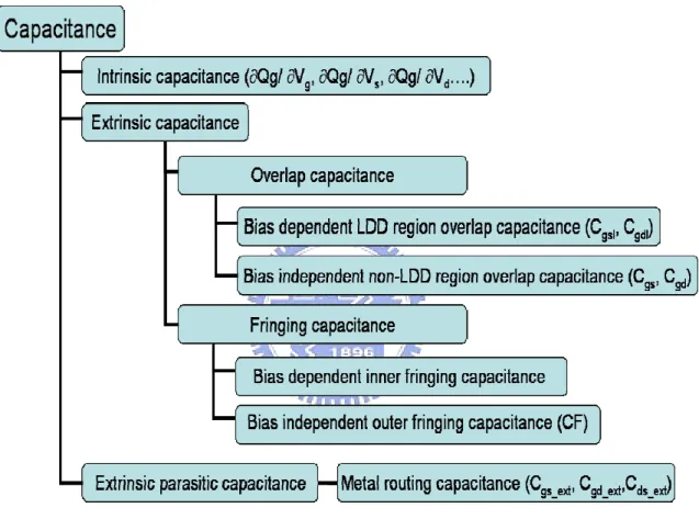
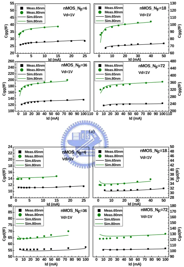
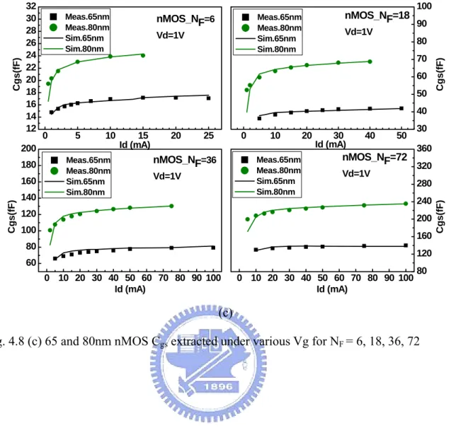
(10) Fig. 3.7. 0.13µm general purpose tech. nMOS with NF =6, 18, 36, 72 biased at Vd = 1.2V and Vg = 0.6V. Pad layout with poly-ground shielding under signal pad. Signal pad metal stacking consists of M8 only. Comparison of noise parameters between as-measured and after correlation matrix de-embedded. (a) NFmin (b) Rn (c) Re(Ysopt) and Im(Ysopt)…………….…... 32 33. Chapter 4 Fig. 4.1. (a) Id-Vd characteristic measured with and without Kelvin connection….... 41. (b) Id-Vg characteristics measured with and without bias-T network to isolate the small-signal from DC measurement…………………...…… Fig. 4.2. Fig. 4.3. (a) Linear Id-Vg of 80 and 65nm nMOS when Vd = 0.05V. (NF = 6, 18, 36, 72)…………………………………………………...... (b) Saturation Id-Vg of 80 and 65nm nMOS when Vd = 1V. (NF = 6, 18, 36, 72)……………………………………………………... 41 42 42. Fig. 4.5. (a) Linear gm-Vg of 80 and 65nm nMOS when Vd = 0.05V. (NF = 6, 18, 36, 72)…………………………………………………….. (b) Saturation gm-Vg of 80 and 65nm nMOS when Vd = 1V. (NF = 6, 18, 36, 72)…………………………………………………….. (a) Id-Vd of 65nm nMOS for Vg = 0~1V with 0.2V Vg step. (NF = 6, 18, 36, 72) ……………………………………………………. (b) Conductance gds-Vd of 65nm nMOS. (NF = 6, 18, 36, 72)…………….. (c) Output resistance Rout-Vd of 65nm nMOS. (NF = 6, 18, 36, 72)………. Transconductance gm for various NF of 65 and 80nm respectively……….... 44 44 45 45. Fig. 4.6. Category diagram of capacitance in MOSFETs……………………………. 46. Fig. 4.7. (a) 65nm nMOS Cgg, Cgd and Cgs extracted at Vg = Vd = 1V for NF = 6, 18, 36, 72……………………………………………………….. 47. Fig. 4.4. Fig. 4.8. (b) 80nm nMOS Cgg, Cgd and Cgs extracted at Vg = Vd = 1V for NF = 6, 18, 36, 72………………………………………………………. (a) 65 and 80nm nMOS Cgg extracted under various Vg for NF = 6, 18, 36, 72………………………………………………………. (b) 65 and 80nm nMOS Cgd extracted under various Vg for NF = 6, 18, 36, 72………………………………………………………. (c) 65 and 80nm nMOS Cgs extracted under various Vg for NF = 6, 18, 36, 72……………………………………………………….. viii. 43 43. 47 48 48 49.
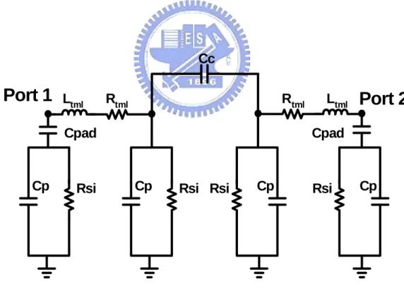
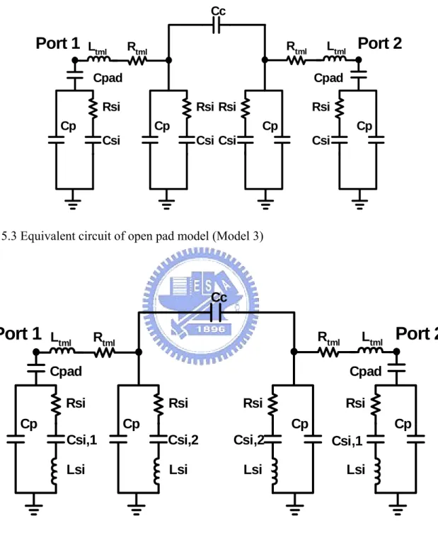
(11) Chapter 5 Fig. 5.1. Equivalent circuit of open pad model (Model 1)………………………….... 57. Fig. 5.2. Equivalent circuit of open pad model (Model 2)………………………….... 57. Fig. 5.3. Equivalent circuit of open pad model (Model 3)………………………….... 58. Fig. 5.4. Proposed equivalent circuit of open pad model (Model 4)……………….... 58. Fig. 5.5. Fig. 5.9. Imaginary part of Y11 measured and simulated by different equivalent open pad model……………………………………………………….......... Magnitude of S11 measured and simulated by different equivalent open pad model………………………………………………………………….. Phase of S11 measured and simulated by different equivalent open pad model…………………………………………………………………......... (a) Equivalent circuit model derivation by circuit analysis……………….. (b) Pad model parameter extraction flow………………………………….. Simulation and measurement of open pad S11, S22, Y11, and Y22…………... Fig. 5.10. MOSFETs device modeling items and modeling flow………………........... 63. Fig. 5.11. Full circuit model MOSFETs device modeling items and modeling flow…. 64. Fig. 5.12. (a) Rg extracted from real part of (Z11-Z12) for 80nm DUT……………….. Fig. 5.13. (b) Rg extracted from real part of (Z11-Z12) for 65nm DUT……………….. Measured and simulation fT for (a) 80nm and (b) 65nm DUT……………... 65 65 66. Fig. 5.6 Fig. 5.7 Fig. 5.8. Fig. 5.14. Fig. 5.15. (a) Measured S11 for gate terminal and good fit by simulation using the proposed RLC circuit. (80nm nMOS with NF = 6, 18, 36, 72)………… (b) Measured S22 for drain terminal and good fit by simulation using the proposed RLC circuit. (80nm nMOS with NF = 6, 18, 36, 72)………… (c) Measured S11 and S22 for gate and drain terminal and good fit by simulation using the proposed RLC circuit. (65nm nMOS with NF = 6, (a) (b). Fig. 5.16. (a) (b). 18, 36, 72)……………………………………………………………… Smith chart of measured S11 for DUT and good match by simulation using proposed circuit (80nm nMOS with NF = 6, 18, 36, 72)………... Smith chart of measured S22 for DUT and good match by simulation using proposed circuit (80nm nMOS with NF = 6, 18, 36, 72)……….. Smith chart of measured S11 for DUT and good match by simulation using proposed circuit (65nm nMOS with NF = 6, 18, 36, 72)………... Smith chart of measured S11 for DUT and good match by simulation using proposed circuit (65nm nMOS with NF = 6, 18, 36, 72)……..... ix. 59 59 60 60 61 62. 66 67. 67 68 68 69 69.
(12) Fig. 5.17. Fig. 5.21. (a) Measured Y11 and Y22 with good fit by simulation of 80nm nMOS…. (b) Measured Y11 and Y22 with good fit by simulation of 65nm nMOS…. Extrinsic results of measured and simulation NFmin, Csi effect is demonstrated for 80nm nMOS (NF = 6, 18, 36, 72)……………………….. Extrinsic results of measured and simulation Rn for 80nm nMOS (NF = 6, 18, 36, 72)………………………………………………………… (a) Extrinsic results of measured and simulation Re(Ysopt) of for 80nm nMOS…..……………………………………………………….. (b) Extrinsic results of measured and simulation Im(Ysopt) of for 80nm nMOS…………………………………………………………… Extrinsic results of measured and simulation NFmin for 65nm nMOS……... Fig. 5.22. Extrinsic results of measured and simulation Rn for 65nm nMOS……….... 73. Fig. 5.23. (a) Extrinsic results of measured and simulation Re(Ysopt) of for 65nm nMOS..…………………………………………………….......... (b) Extrinsic results of measured and simulation Im(Ysopt) of for. 74. Fig. 5.18 Fig. 5.19 Fig. 5.20. Fig. 5.24. Fig. 5.25. Fig. 5.26. 65nm nMOS…………………………………………………………… (a) Extrinsic results of measured and simulation NFmin under various drain current at frequency 2.4GHz, 5.8GHz, and 10GHz for 80nm nMOS………………………………………………………………….. (b) Extrinsic results of measured and simulation NFmin under various drain current at frequency 2.4GHz, 5.8GHz, and 10GHz for 65nm nMOS…. Extrinsic results of measured and simulation Re(Ysopt) and Rn under various Id at frequency 2.4GHz, 5.8GHz, an 10GHz for 65nm nMOS (NF = 6, 18, 36, 72)………………………………………………………… Extrinsic results of measured and simulation Im(Ysopt) under various Id at frequency 2.4GHz, 5.8GHz, an 10GHz for 65nm nMOS (NF = 6, 18, 36, 72)…………………………………………………………. 70 70 71 71 72 72 73. 74. 75 75. 76. 76. Chapter 6 Fig. 6.1 Fig. 6.2 Fig. 6.3 Fig. 6.4. Extrinsic measured and intrinsic simulation Rn for 80 and 65nm nMOS (NF =6, 18, 36, 72)……………………………………………..................... Extrinsic measured and intrinsic simulation Re(Ysopt) for 80 and 65nm nMOS (NF =6, 18, 36, 72)……………………………………………......... Extrinsic measured and intrinsic simulation Im(Ysopt) for 80 and 65nm nMOS (NF =6, 18, 36, 72)……………………………………………......... Extrinsic measured and intrinsic simulation NFmin for 80 and 65nm nMOS (NF =6, 18, 36, 72)……………………………………………..................... x. 82 82 83 83.
(13) Fig. 6.5. Fig. 6.10. Intrinsic simulation NFmin for 80 and 65nm nMOS biased in its maximum gm and minimum NFmin condition (NF =6, 18, 36, 72)…….......................... Intrinsic simulation NFmin for 80 and 65nm nMOS biased under varying Id at 2.4GHz, 5.8GHz and 10GHz (NF =6, 18, 36, 72)……….......................... Intrinsic simulation Rn for 80 and 65nm nMOS biased under varying Id at 2.4GHz, 5.8GHz and 10GHz (NF =6, 18, 36, 72)………………………... Intrinsic simulation Re(Ysopt)for 80 and 65nm nMOS biased under varying Id at 2.4GHz, 5.8GHz and 10GHz (NF =6, 18, 36, 72)…………………… Intrinsic simulation Im(Ysopt)for 80 and 65nm nMOS biased under varying Id at 2.4GHz, 5.8GHz and 10GHz (NF =6, 18, 36, 72)…………………… Rg effect on NFmin. NFmin simulated by intrinsic model with and w/o Rg….. Fig. 6.11. Rg effect on Rn. Rn simulated by intrinsic model with and without Rg.......... 87. Fig. 6.12. Rg effect on Sig. Sig simulated by intrinsic model with and without Rg……. 88. Fig. 6.13. Ratio of Sig simulated by intrinsic model w.r.t. Sig calculated by. Fig. 6.14. 4kBT∆Rg(ωCgg)2............................................................................................ Rg effect on Sid. Sid simulated by intrinsic model with and without Rg……. Fig. 6.15. Ratio of Sid simulated by intrinsic model w.r.t. Sid calculated by. Fig. 6.16. 4kBT∆Rggm2….............................................................................................. Comparison of Sig and Sid of simulated intrinsic model……………………. Fig. 6.6 Fig. 6.7 Fig. 6.8 Fig. 6.9. 84 85 85 86 86 87. 88 89. 89 90. Appendix A Fig. A.1. Presentation of a noisy two-port network connected to a noise source and source admittance…………………………………………………………... 96. Appendix D Fig. D.1. Equivalent circuit of test structure with DUT…………………………….... 104. Fig. D.2. Equivalent circuit of open pad…………………………………………….... 105. Fig. D.3. Equivalent circuit of short pad……………………………………………... 105. xi.
(14) Table Captions Chapter 4 Table 4.1. Model parameters for gate capacitance modeling…………………….... 40. Table 5.1. Open pad model parameters……………………………………………. 53. Table 5.2. Pad model parameters for various NF after optimization………………. 55. Chapter 5. xii.
(15) Chapter 1 Introduction The aggressive scaling of CMOS technologies has resulted in remarkable improvement in the RF performance. Accompanied with its superiority in low cost, high integration and mature techniques, CMOS has become a promising candidate for RF circuit application. The rapid growing wireless communication industry and its severe competition increase the needs for RF chips and demand the reduction of product design cycle. Accuracy of the device model is one of the important factors that affect the circuit performance and its success. The complex signal coupling inside the device and the lossy characteristic of silicon substrate make parameter extraction and device modeling a challenge.. 1.1 Motivation In the last decade, there have been increasing studies focusing on RF CMOS parameter extraction and modeling. Among them, many researches tend to solve two of most key items that affect the RF performance, gate resistance and substrate network. Many approaches have been proposed to model these two key features. However, a standard extraction and modeling method have not been established yet. Another challenge in the field of RF CMOS gained more and more attraction recently is the noise modeling. The demand of accurate prediction of noise behavior comes from the low power and low noise RF chips for portable communication and some medical applications. On-wafer measurement at microwave frequency is the best way to characterize the RF device. However, as we all know, measurement of high frequency characteristics always incorporated parasitic effects introduced by the test feature excluding the device of major interest. Accurate de-embedding procedure prior to parameter extraction and device modeling 1.
(16) can isolate those parasitics and generally make model more scalable. Therefore, de-embedding of parasitic components is also one of the important works. Regarding low noise RF CMOS design, noise modeling is absolutely more challenging than S-parameters modeling. The difficulty is due to the complex noise mechanism in MOSFET, limited knowledge about the noise source, and coupling introduced by low resistivity Si substrate. In recent years, many studies have been focused on noise current extraction [1] and noise mechanism modeling [2-5]. However, fewer studies were focused on the noise de-embedding and intrinsic noise extraction [6,7]. Noise de-embedding is also considered as an important procedure prior to noise modeling and simulation. In the research process, some suspicious features occurred in the as-measured noise characteristics. It suggests that appropriate de-embedding is indispensable. This stimulates our motivation of this study on the noise de-embedding techniques and triggers some new ideas proposed in this thesis.. 1.2 Overview The main objective of this thesis is to deal with one of important issues in MOSFET noise modeling, it is noise de-embedding. To achieve this goal, detailed information about MOSFET noise in terms of theoretical principle, measurement data and simulation results will be provided. This thesis has been organized into seven chapters as follows: Chapter 2 gives an introduction to the classification and physical mechanism of noise in MOSFETs. The noise measurement theory and measurement system configuration are also covered. Chapter 3 begins with discussion of as-measured noise parameters and three interesting features identified in this study. In the following, conventional correlation matrix de-embedding method and its usability will be reviewed. Chapter 4 presents the intrinsic model calibration in terms of I-V characteristics and gate capacitance feature, which were extracted from de-embedded Y-parameters at low frequency. 2.
(17) Key model parameters associated with I-V and C-V in BSIM model are discussed. Chapter 5 addresses how to build the lossy pad equivalent circuit model associated with various layout structures. The extensive verification on full circuit model will be described. Good match with the measured extrinsic noise characteristics will be demonstrated. Chapter 6 discusses the equivalent circuit noise de-embedding results in which intrinsic noise performance for sub-100nm MOSFET has been extracted. It helps to identify the truly intrinsic performance of the devices and provide the circuit designers correct guideline for low noise design. Chapter 7 concludes with a summary and suggestions for future work. Appendices A ~ D provide more detailed explanation of certain contents. Appendix A describes the derivation of noise parameters. Appendix B addresses the Y-factor method for noise figure measurement. Appendix C interprets the noise correlation matrix de-embedding technique. Finally appendix D provides the modified open and short de-embedding method.. 3.
(18) Chapter 2 Noise Theory and Noise Measurement Technique Noise, briefly speaking, can be thought as a kind of signal that is undesirable for a device, circuit, or system. It is generally caused by the fluctuation of voltage or current in an electronic device or component. Noise set the lower limit of measurement or detection which is an important issue for engineering application. In this chapter, noise sources in electronic devices are summarized and high frequency noise in MOSFET, which is dominated by the thermal noise, is focused. Noise theory for noise behavior analysis of two-port network will be covered. Finally, high frequency noise characterization and analysis are provided in the end of the chapter.. 2.1 Noise Sources The most important sources of noise in electronic devices are shot noise, generation-recombination noise, flicker noise and thermal noise. Shot noise is generated when carriers in device cross barriers independently and randomly. It is an eminent noise source for diodes and bipolar transistors. For MOSFETs, only DC gate leakage current contributes shot noise. However, gate leakage is normally controlled to be very small. Generation and recombination noise occurs in semiconductors in which traps and recombination centers are always involved. Fluctuation of carrier number due to random trapping and de-trapping process contributes this noise. The dominant noise sources of MOSFETs are flicker noise and thermal noise. The origin of flicker noise is generally proposed coming from the carrier number fluctuation due to trapping and de-trapping processes in the Si-SiO2 interface or from mobility fluctuation of device on the basis of empirical results. It is also called, 1/f noise, due to its noise power 4.
(19) spectral density given by (2.1) in which a frequency dependence with slope n approaching unity is achieved. Im SI ( f ) = K ⋅ n f. (2-1). However, while working in microwave frequency, flicker noise is small compared with thermal noise. Therefore, thermal noise is the main concern for RF CMOS operation. Nevertheless, for some RF applications such as mixers or oscillators where low frequency signal may be converted up to an intermediate or high frequency, and deteriorate the phase noise and signal-to-noise ratio. 2.1.1 Thermal Noise Thermal noise is originated from the current fluctuation caused by collision of lattice and carriers by means of random thermal motion. Thermal motion of carriers is ubiquitous in any electronic components as long as its temperature is not absolute zero. Because of the thermal nature, thermal noise power turns out to be exactly proportional to temperature. Starting from the quantum theory of a harmonic oscillator, available noise power of thermal noise is given by [7]. 1 hf Pav = [ hf + ( hf / kT ) ] ⋅ ∆f 2 e −1. (2-2). where h is Plank’s constant, k is Boltzmann’s constant, f is the operating frequency and ∆f is the frequency interval. For hf/kT << 1 (holds for general case) and based on the noisy resistor model shown in Fig. 2.1, the mean-square open circuit noise voltage and noise current can be obtained. Pav = kT ∆f =. v n2 4R. (2-3). v n2 = 4kTR ∆f. (2-4) 5.
(20) i n2 =. 4kT ∆f = 4kTG∆f R. (2-5). Every component with electrical resistivity can be considered as a resistor. With known resistance value or equivalent resistance, noise voltage or noise current can be calculated. 2.1.2 Thermal Noise in MOSFETs In MOSFETs, noise components include channel noise (or called drain current noise), induced gate noise and thermal noise due to terminal parasitic resistances (Rg, Rd, Rs). The most broadly accepted noise model for MOSFETs is the van der Zeil model [8]. For a MOSFET under operation, the conducting channel behaves like a voltage-controlled resistor. This resistor contributes thermal noise at the drain terminal. The power spectral density can be derived from the drain current expression. Refer to Fig. 2.2, taking velocity saturation into consideration, drain current at a certain position along channel direction is given by [7] ⎛ I (x) ⎞ dV I D (x) = Weff ⋅ Q I (x) ⋅ν (x) = ⎜ µeff ⋅ Weff ⋅ Q I (x)- D ⎟ ⋅ E C ⎠ dx ⎝. (2-6). Integrating this current over the effective channel Leff, drain current can be obtained. ID =. 1 Leff. ∫. VD. VS. ⎛ ID ⎞ ⎜ µeff ⋅ Weff ⋅ Q I (V)⎟ ⋅ dV EC ⎠ ⎝. (2-7). The mean square values of a current fluctuation ∆i d (t) caused by ∆v(t) in a unit length segment is 1 (∆i d ) = 2 Leff 2. 2. ⎛ ID ⎞ 2 ⎜ µeff ⋅ Weff ⋅ Q I (V)⎟ ⋅ (∆v) E C ⎠ ⎝. where (∆ν ) 2 is. 6. (2-8).
(21) (∆ν ) 2 =. 4kTe ( x i ) ⋅ ∆x ⎛ ID ( x i ) ⎞ ⎜ µeff ⋅ Weff ⋅ Q I (x i )⎟ EC ⎠ ⎝. ∆f (2-9). Finally, power spectral density of the noise current generated by the channel resistance includes velocity saturation effect and hot-electron effects is given. SId =. (i d ) 2 4k = 2 Leff ⋅ I D ∆f. ∫. VD. VS. ⎛ I ⎞ Te ( x ) ⎜ µeff ⋅ Weff ⋅ Q I (V)- D ⎟ ⋅ dV EC ⎠ ⎝. (2-10). where Te is the effective electron temperature in which hot-electron effect is considered. This is a general expression for the thermal noise in a channel. For simplicity it can be written as. SId =. (i d ) 2 =4kTγ g d0 ∆f. (2-11). where gd0 is the drain transconductance at VDS is zero. For long channel devices, γ is close to unity in its triode region and decreases to about 2/3 when in saturation (i.e.. 2 ≤ γ ≤ 1 ). 3. In long channel case, gd0 is equal to the gate transconductance gm in saturation region which leads to a familiar result. (id ) 2 8 8 SId = = kTg d0 = kTg m ∆f 3 3. (2-12). Due to the carrier heating by the large electric fields in short channel devices, γ may become larger than 2 and even larger. Besides the channel current noise, the induced gate noise has gained increasing attention. As the operation frequency increases, contribution of this noise can not be neglected. Noise model including this terms, thus, become essential. Induced gate noise is, as implied by the name, the noise induced by capacitive coupling from channel region to gate terminal due to the fluctuating potential. This noise can be expressed as [9] 7.
(22) SIg =. (i g ) 2 ∆f. (2-13). =4kTγ g g. where gg is given by. gg =. ω 2 Cgs2. (2-14). 5g d0. Because the channel noise and induced gate noise have a common origin, they do have correlation. The correlation coefficient is usually expressed as. c=. i g i*d. (2-15). i g2 i d2. As for noise contributed from parasitic resistances, they follow (2-5) and are given by SI,Rg =. 4kT 4kT 4kT ; SI,Rd = ; SI,Rs = Rg Rd Rs. (2-16). Among them, due to the larger sheet resistance of poly-Si, gate resistance (Rg) is typically much larger than drain and source resistance (Rd and Rs). Therefore, Rg is an important noise contributor which can greatly affect the noise figure of the device. Multi-finger gate structure is widely used in RF MOSFET design to reduce Rg. Not only noise behavior, several characteristics are related to Rg too, in which maximum oscillation frequency (fmax) is one of the example. Multi-finger gate gain some performance but pay the penalty of larger parasitic capacitance.. 2.2 Two-Port Noise Theory 2.2.1 Noise Figure. As mentioned above, overall noise of a device is generally not from a single origin. It does need a simpler measure of noise performance. For device characterization and circuit 8.
(23) design application, noise figure or noise factor is the most popular expression used. Based on the two-port noisy network model and definition of noise figure, formula of noise parameters can be derived. Noise factor is defined as the signal-to-noise power ratio at the input to the signal-to-noise power ratio at the output. F ≡. Si /N i So /N o. (2-17). From this definition, we can understand that noise factor of a network depicts the degradation of signal-to-noise ratio as signal goes through this network. Considering a network with gain G and noise Na, noise factor then can be express as F ≡. N +GN i Si /N i Si /N i = = a So /N o GSi /(N a +GN i ) GN i. (2-18). where Na and G are the noise power and gain of the network. From the expression shown above, noise factor can be defined as the ratio of total noise power at the output to the output noise power which is due to the input noise. In short, the larger noise factor means the noisier of the network. In (2-18), it shows the value of noise factor is affected by the input noise power which is generally from the thermal noise of the source, kT∆f. This means noise factor depends on the source temperature. 290K was adopted as a standard temperature by IEEE because it makes the value of kT close to around 4 × 10-21 Joule. Generally we use this measure in the unit of dB, named noise figure. NF = 10 log F. (2-19). 2.2.2 Noise Parameters. Further detail derivation of noise factor based on the noise model with noise sources at the input leads to the following expression [10] 9.
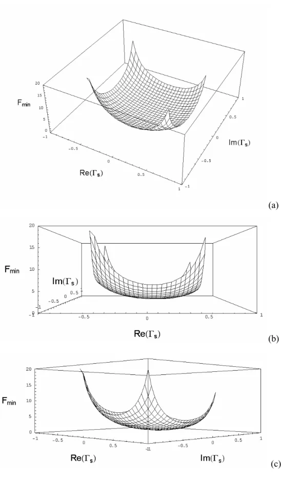
(24) F = Fmin +. R n Ys -Yopt. 2. (2-20). Gs. where Ys = G s +j Bs. (2-21). Yopt = G opt +j Bopt. (2-22). Here Ys is the source admittance, Gs is the real part of Ys, Yopt is the optimum source admittance, and Fmin is the minimum noise factor achieved in the network when the source admittance Ys is equal to Yopt. Rn is named the equivalent noise resistance which indicates how sensitive the noise factor is when Ys differs from Yopt. Replacing the source admittance with its corresponding reflection coefficient at specific characterization impedance Z0, another common form of noise factor is obtained 2. Γs -Γopt 4R F = Fmin + n Z0 (1 − Γ 2 ) 1+Γ opt opt. Yopt =. Ys =. 1 1-Γopt Z0 1 + Γ opt. 2. (2-23). (2-24). 1 1-Γs Z0 1 + Γ s. (2-25). This gives us an idea that the noise figure of the network is not only determined by noise source inside but also the source admittance (Ys) driving it. It is also our goal to get the smaller noise factor while keep sufficient gain by varying Ys. The so-called noise parameters are the four parameters Fmin, Rn, Re(Γopt) and Im(Γopt). These parameters are determined purely by the intrinsic noise source of the network, they are unique under a certain operation frequency and bias. Typical dependence of noise figure on source admittance at a fixed 10.
(25) frequency and bias is a 3-D parabolic curve (x-y-z axis: Re(Γopt)-Im(Γopt)-Fmin), Rn is the curvature. Fig. 2.3 and Fig. 2.4 give noise factor plotted with respect to Re(Γopt) and Im(Γopt) with Fmin = 1, Re(Γsopt) = Im(Γsopt) = 0.1 and Rn = 100 and 50 (Ω) respectively. They give a simple idea about the noise figure characteristics.. 2.3 Thermal Noise Model There are two models for channel thermal noise model supported by BSIM3v3.2.2. One is SPICE2 noise model and the other is BSIM3v3 noise model. Noise model flag is defined to invoke different noise model sets [11]:. Noise model selection was done by parameter noimod. Both flicker noise and thermal noise can be calculated using SPICE2 or BSIM3v3 model. Detailed equations for flicker noise are not covered in this thesis and they can be referred to BSIM3v3 manual. Another noise model supported by many simulators is the HSPICE model. In Agilent-ADS simulator, BSIM3 model selected by noimod is valid when NLEV < 1 or HSPICE model will be used according to NLEV values (NLEV=1, 2, or 3). In models mentioned above, velocity saturation and the hot-electron effect model which are considered as two important effects in sub-micron transistors were not included. SPICE2 Model. For noimod = 1 or 3, thermal noise is calculated according to [12] SId =. 8kT (g m + g ds + g mbs ) 3. 11. (2-26).
(26) This model is the modification of old HPSICE model shown below as with NLEV < 3, which improves the model accuracy in linear region. BSIM3v3 Model. If noimod = 2 or 4, thermal noise power spectral density is calculated by [13] SId =. 4kT µeff Qinv L2eff. (2-27). where Qinv is the channel inversion charge calculated according to the capacitance models (capMod=0, 1, 2, or 3). HSPICE Model. The HSPICE noise model has different equations to calculate the flicker and thermal noises. Equation selection is through a parameter, NLEV. For NLEV smaller than 3, different flicker noise model was used but the same thermal noise equation was implemented which is given by [14] SId =. 8kT ⋅ g m 3. (2-28). which is an old model and is lack of accuracy for modern devices. If NLEV is set to 3, the noise equation is then given by [13] SId =. 8kT 1 + a + a2 ⋅ β ⋅ (VGS − VT ) ⋅ ⋅ Gdsnoi 3 1+ a. (2-29). where. β=. Weff ⋅ µeff ⋅ Cox Leff. a = 1− = 0,. (2-30). VDS , Linear region VDSAT Saturation region 12. (2-31).
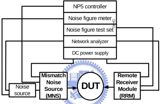
(27) and Gdsnoi is the thermal noise coefficient with default value equal to 1. Models mentioned above are integrated into various commercial simulators. Many other models have been proposed to consider velocity saturation effect, hot-electron effect or both [4, 5]. But they are not yet well accepted and verified. Noise simulation result comparison of different models was done in [15]. In this thesis, HSPICE model with NLEV set to 3 was used.. 2.4 High Frequency Noise Measurement In this work, high frequency noise measurement was supported by Radio Frequency Technology Center of National Nano Device Laboratory (NDL RFTC). On-wafer noise characterization was conducted using NP5 series noise parameter measurement system. The measurement system is introduced as follows. 2.4.1 System Configuration [16]. High frequency noise measurement system is mainly composed of a noise figure meter (HP8970B), network analyzer (HP8510), DC power supply (HP4142), a controller unit (NP5B controller), two remote modules (MNS and RRM), and a noise source. Block diagram of system configuration is shown in Fig. 2.5. Port 1 of the system is connected to device-under-test (DUT) by means of a coplanar probe through a mismatch noise source (MNS). MNS is a solid state electronic tuner with a built-in bias-Tee and switching circuit. Output port (Port 2) of the DUT is followed by a remote receiver module (RRM), which consists of a low noise amplifier (LNA), bias-Tee and switching circuit. The LNA improves noise characterization accuracy by providing a low noise second stage. Noise source is the noise power supply connected at port 1 defined by its ENR (excess noise ratio) value. The ENR expresses the difference in noise power out of the noise source when it is “on” (hot state) and when it is “off” (cold state).. 13.
(28) 2.4.2 System Calibration and Measurement. As high frequency characterization was conducted on the devices (DUT), the applied signals with short wavelength are comparable to the probe, connecting cables, adapters, bonding wires, and our interested device. Thus, losses caused by the connections will remarkably affect the measurement results, especially critical as measurement frequency increases. On the other hand, a measurement system has its own system error. Consequently, a system calibration should be performed to take those losses into consideration, calibrate the system errors and then shift the measurement signal reference plane to the DUT plane. The validity and accuracy of the calibration results depend on the calibration method used. For S-parameter measurement, SOLT (short-open-load-through) calibration is a popular method to establish the DUT test plane nowadays. For the noise measurement system, there are several calibration steps required to build a noise measurement plane for DUT. A complete calibration procedure includes input SOL calibration, noise source calibration, network analyzer calibration, thru delay calibration, RRM calibration, MNS calibration and finally system noise parameter calibration. Since calibration details are not our focus, only rough idea is provided here. After the overall calibration procedure, noise contribution of the system will be characterized. Thus, real noise power of DUT can be separated from the noise power contributed from system. This can be verified by connecting the input and output with a known DUT, in our case a dummy “thru” pattern was used to check if the noise figure is less than 0.1dB. After calibration, noise measurement reference plane is then established. In the beginning of noise parameter characterization, S-parameters measurement at the DUT reference plane should be done first. In the following, by varying the impedance presented to the input of the DUT around the Smith chart, output noise power (sometimes, also refers to noise temperature) of DUT plus the receiver as a function of Γs (source reflection coefficient) 14.
(29) was measured, each Γs and the corresponding noise power constructs a set of equations. The noise parameters are decided by solving the set of equations. Theoretically speaking, only four input states are needed for noise characterization because the noise behavior equation (2-23) has merely four unknown parameters. In practice, however, for the sake of reducing the influence of random errors more than four points were measured (generally 16 states or 20 states) and a proper fitting procedure was used to extract the parameters. Finally, four noise parameters: NFmin, Rn, Re (Γopt) or Re (Yopt) and Im (Γopt) or Im (Yopt) are obtained. In the measurement process, the overall noise figure was calculated by Y-factor method technique. The overall noise figure is then under a noise figure correction step to determine the noise figure of the DUT. Details of Y-factor method and noise figure correction are included in Appendix B.. 15.
(30) R R. vn +-. R. vn +-. (a). in. (b). R. (c). Fig. 2.1 (a) Equivalent network for computing thermal noise of a resistor.(b)(c) Thermal noise model for a resistor.. W Gate L. QI (x). Source. Drain. v(x). E, lateral field. P-substrate. 0. x x+dx. Leff. Fig. 2.2 Schematic diagram of a MOSFET operated in saturation condition.. 16.
(31) (a). (b). (c). Fig. 2.3 (a)(b)(c) noise figure F plotted with respect to Re(Γopt) and Im(Γopt) with Fmin = 1, B. Re(Γsopt) = Im(Γsopt) = 0.1 and Rn = 100. B. B. B. B. B. B. 17. B. B. B. B. B.
(32) (a). (b). (c) Fig. 2.4 (a)(b)(c) noise figure F plotted with respect to Re(Γopt) and Im(Γopt) with Fmin = 1, B. Re(Γsopt) = Im(Γsopt) = 0.1 and Rn = 50. B. B. B. B. B. B. 18. B. B. B. B. B.
(33) NP5 controller Noise figure meter Noise figure test set Network analyzer DC power supply. Noise source. Mismatch Noise Source (MNS). DUT. Remote Receiver Module (RRM). MNS: A solid state electronic tuner with embedded bias-T and switching circuit. RRM: A low noise amplifier with embedded bias-T and switching circuit. Fig. 2.5 Block diagram of ATN noise figure measurement system configuration.. 19.
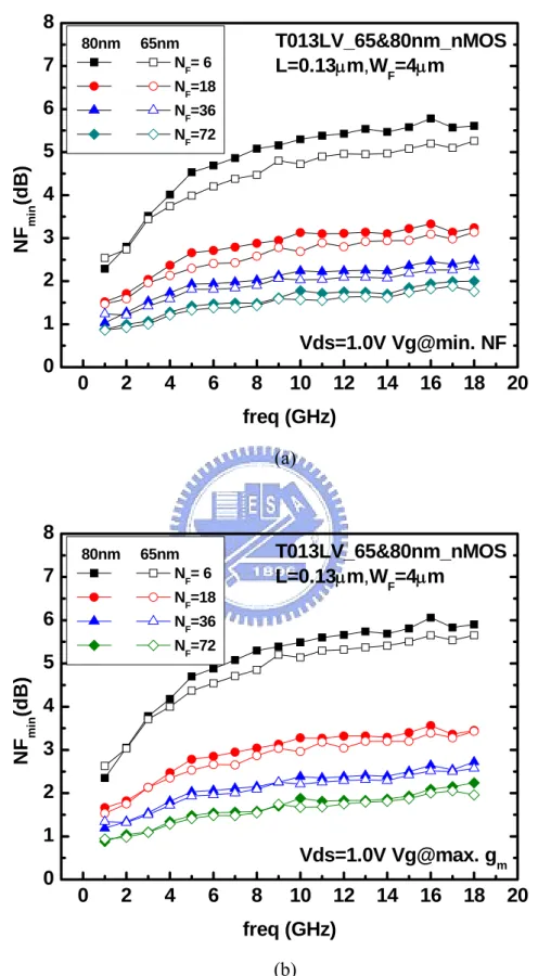
(34) Chapter 3 RF MOSFET Noise Characterization 3.1 Extrinsic Noise Characteristics RF MOSFETs with 80nm and 65nm gate length were fabricated to study the nanoscale CMOS scaling effect on speed and noise performance. Multi-finger structure with fixed finger width (4µm) and various finger numbers (NF=6, 18, 36, 72) are employed to reduce the gate resistance. Reduction of gate resistance shows no impact on cut-off frequency (fT). fT =. gm 2 2 2π Cgg − Cgd. (3-1). while other RF performance can be improved such as maximum oscillation frequency (fmax) and noise figure (NFmin) [17,18]. Fig. 3.1 indicates Rg extracted from Z-parameters and gate capacitances (Cg) extracted from Y-parameters for various finger numbers. It shows a trade-off between Rg and Cg (Cgd, Cgs). Measured NFmin for 65nm and 80nm nMOS of various NF are shown in Fig. 3.2 (a) and (b). One is biased under maximum gm (Vgs = 0.7V for 80nm and Vgs = 0.6V for 65nm) which is corresponding to maximum fT, the other is biased under minimum NFmin (Vgs = 0.55V for 80nm and Vgs = 0.35V for 65nm). They indicate there is certain gate voltage difference between maximum fT and minimum NFmin. NFmin without de-embedding decreases remarkably with increasing NF. One reason is the Rg reduction due to increase multi-finger gate number, however, this can not explain the dramatic difference such as 2.5~3dB between NF = 6 and NF = 72 in frequency range of 5~18GHz. Fig. 3.3 illustrates the fT extracted from extrapolation of |H21| to unity gain. Rg is decreasing as NF increases at the expense of larger gate capacitance. (3-1) shows fT is 20.
(35) dependent on gm and gate capacitance. Both gm and Cg are nearly proportion to the finger number, thus lead to weak dependence on NF for fT at around 100~105GHz for 80nm device. Scaling from 80nm to 65nm in gate length, about 20~30% increase in driving current and maximum transconductance and 20% reduction in gate capacitance lead to obvious 50~60% improvement in maximum fT. The improvement indicates the advantage provided by device scaling for high speed CMOS applications. However, measured NFmin of these two sets of devices did not show significant difference. Three interesting features are revealed in measured noise in Fig. 3.2. Firstly, there is an abnormal strong dependence on finger number while fT is almost the same thought Rg is reduced. Secondly, weak dependence on gate length was observed even gained 50% fT improvement. The last is the nonlinear frequency dependence of NFmin which can not be explained by the theoretical thermal noise behavior. As expressed in equivalent circuit element, NFmin was shown to be linearly dependent on frequency [18-20]. Consequently, it is suggested that lossy pad and lossy substrate contribute to these excess noise. Noise is coupled from the lossy substrate through capacitive probing pad and interconnects transmission line. To understand the pure noise behavior (intrinsic) of the DUT and further to model it, noise de-embedding on the measured one is indispensable.. 3.2 Conventional Noise De-embedding Method Conventionally, there are two ways to characterize the intrinsic noise performance of MOSFET transistors. One is by directly de-embedding the external noise through matrix calculation that is similar to the S-parameter de-embedding but much more complicated. This popular technique is called noise correlation matrix de-embedding. The other method is to extract intrinsic noise parameters through the approach of equivalent circuit model. This is a new method developed in this study. By equivalent circuit implementation, measured noise parameters can be simulated and noise caused by probing pad can also be characterized. The 21.
(36) details will be described in chapter 5. 3.2.1 Noise Correlation Matrix De-embedding. According to the circuit theory of linear noisy networks, any two-port device can be separated into two parts: additional noise source part and noiseless device part. For common application three equivalent representations are used to describe the two-port devices, they are admittance, impedance, chain representation respectively [21]. Generally, chain representation is used mostly in which a voltage noise source and a current noise source are included. Chain representation of a noisy two-port network is shown in Fig. 3.4. The benefit of the representation is that it is easier to find the relation of input signal and noise level because it refers the entire device noise source to the input. Correlation matrices are described with the noise sources in the form of self-power and cross power spectral densities as matrix element. Power spectral densities are defined as the Fourier transform of their auto and cross correlation function. To perform noise de-embedding, correlation matrices of the two-port circuit and the decomposed components should be known. The matrices are obtained from the measured noise parameters or calculated theoretically based on the physics (such as those passive elements). The noise parameters of a passive device are fully determined by its small-signal parameters. For an element with admittance Y, the correlation matrix is given in the form of. C Y =2K BT ⋅ Re[Y]. (3-1). Chain representation of the whole test fixture is estimated from the measured noise parameter (NFmin, Rn, Yopt). ⎛ Rn ⎜ [CA ] = 2K BT ⎜ ⎜ Fmin − 1 − R Y * ⎜ n opt ⎝ 2 22. Fmin − 1 ⎞ − RnYopt ⎟ 2 ⎟ 2 ⎟ Rn | Yopt | ⎟ ⎠. (3-2).
(37) Once the correlation matrices are known, according to the configuration of the two-port network, transformation of correlation matrices should be done. Appropriate matrix operation is applied to isolate the parasitic parts form the intrinsic correlation matrix. Noise parameters after de-embedding, called intrinsic noise parameters, and then could be computed as function of correlation matrix. Fmin,DUT = 1 +. Re[CA,12,DUT ] kBT. +. CA,11,DUT CA,22,DUT − (Im[CA,12,DUT ])2. Ysopt ,DUT = Gsopt ,DUT + Ι * Bsopt ,DUT =. Rn,DUT = Re[. CA,11,DUT 2kBT. kBT. CA,11,DUT CA,22,DUT − (Im[CA,12,DUT ])2 + Ι * Im[CA,12,DUT ] CA,11,DUT. (3-3). (3-4). (3-5). ]. Details of correlation matrices de-embedding procedure are included in Appendix B. 3.2.2 De-embedding Results. For the purpose of studying the correlation matrix de-embedding on different devices. Three test-keys with different probing pad layout structures were implemented. The first one is 0.13µm low voltage technology (013LV) adopted for fabrication of 80nm and 65nm nMOS. The second one is RF CMOS technology using 0.13µm general purpose process (013G) with device target gate length at around 105nm. The last one is also a 0.13µm general purpose technology with target gate length at around 110nm. The three sets of DUT are all nMOS devices but with different probing pad layout structures. Details of these test structures will be discussed in Chapter 5 where the corresponding equivalent circuit will be introduced. De-embedding work was done by writing equations in ADS data display window. The correlation matrix de-embedding results are shown in Fig. 3.5 ~ Fig. 3.7. In Fig. 3.5(a), NFmin after matrix de-embedding show great amount of reduction and almost the same level for 23.
(38) various NF devices. But decrease of NFmin with increasing frequency in lower frequency region (3~5GHz) fails to follow the linear frequency dependence. Reduction of Rn is decreasing as NF increases. The results suggest that more parasitic effect was originally suffered by smaller device, i.e. NF = 6 than NF = 72, and can be eliminated through de-embedding. Reduction of real part of optimum source admittance, Re(Ysopt) was also appreciable and this also relates to the reduction of NFmin. Fig. 3.6 is the comparison of de-embedding results for lossy pad and normal pad test structures. Much more noise reduction for lossy pad than normal pad was observed. It suggests effective de-embedding realized for lossy pad. However, frequency dependence issue as shown in Fig. 3.5 still remains. As for pad structure with poly ground shielding under signal pad, less substrate coupling effect leads to small difference between as-measured data and de-embedded results. In summary, no need to establish an equivalent circuit model required for the matrix correlation method makes it convenient to calculate the intrinsic noise parameters from the measured ones. But there are three major drawbacks make this method not that popular. Firstly, the data after de-embedding usually suffer severe fluctuation due to its limited measurement precision, i.e., de-embedded results are very sensitive to measured data accuracy, especially for novel devices with noise figure below 1dB. The second one is its critical dependence on open pad test structure design and limitation in fully extracting the TML induced extra coupling noise provided that it lacks of ground shielding. The last one drawback is its failure of full range coverage for circuit design application. Because noise parameters and S parameters corresponding to arbitrary biases or frequencies can not be predicted from the measured data limited to certain specified bias and frequency.. 24.
(39) 35. 450. NF= 6. 400. NF=18. 350. NF=36. 300. NF=72. T013LV_80nm_nMOS L=0.13µm,WF=4µm 30. 25 20. 250 200. 15. 150. 10. 100. 5. 50 0. Rg ( Ω). Cgs+Cgd, Cgs, Cgd (fF). 500. 0. 10. 20. 30. 40. 50. 60. 70. 0 80. Finger Number, NF Fig. 3.1 80nm nMOS Rg and Cg (Cgs, Cgd, Cgd) extracted from Z- and Y- parameters. (NF = 6, 18, 36, 72). 25.
(40) 8 80nm. T013LV_65&80nm_nMOS L=0.13µm,WF=4µm. 65nm NF= 6. 7. NF=18. 6. NF=36 NF=72. NFmin(dB). 5 4 3 2 1. Vds=1.0V Vg@min. NF. 0. 0. 2. 4. 6. 8. 10. 12. 14. 16. 18. 20. freq (GHz) (a). 8 80nm. T013LV_65&80nm_nMOS L=0.13µm,WF=4µm. 65nm NF= 6. 7. NF=18. 6. NF=36 NF=72. NFmin(dB). 5 4 3 2 1 0. Vds=1.0V Vg@max. gm 0. 2. 4. 6. 8. 10. 12. 14. 16. 18. 20. freq (GHz) (b) Fig. 3.2 Measured noise figure NFmin of 80 and 65nm nMOS for NF = 6, 18, 36, 72 (a) Vd=1V, Vg at min. NFmin (Vgs=0.7/0.6V)(b) Vd=1V, Vg at max. gm (Vgs=0.5/0.35V). 26.
(41) 200. Cut-off frequency, fT(GHz). 180 160. T013LV_65nm&80nm_nMOS L=0.13µm,WF=4µm. 140 Vds=1.0V 120 100 80 65nm. 60. NF=18. 40. NF=36. 20 0. 80nm NF= 6. NF=72. 1. 10. 100. Id (mA) Fig. 3.3 Cut-off frequency fT of 80 and 65 nm nMOS under various drain current extracted from extrapolation of |H21| = 1.. Vn Noisy Two-Port Network. In. Noiseless Two-Port Network. Fig. 3.4 Chain representation of a noisy two-port network with a voltage source and a current source in the input port.. 27.
(42) 5.0. 8. 013LV_nMOS WF=4µm,NF=6. 7. Measure Matrix De-embedded. 4.0 3.0. 4. 2.5. 3. 2.0 1.5 1.0. 1 0. NFmin (dB). 3.5. 5. 2. 0.5 0. 2. 4. 6. 8. 4.0. 013LV_nMOS WF=4µm,NF=36. 3.5 3.0 NFmin (dB). 4.5. 10 12 freq (GHz). 14. 16. 18. 20. 0. 2. 4. 6. 8. 013LV_nMOS WF=4µm,NF=72. Measure Matrix De-embedded. 10 12 14 freq (GHz). 16. 18. 0.0 20 3.0. Measure Matrix De-embedded. 2.5 2.0. 2.5 2.0. 1.5. 1.5. 1.0. NFmin (dB). NFmin (dB). 6. 013LV_nMOS WF=4µm,NF=18. Measure Matrix De-embedded. 1.0 0.5. 0.5 0.0. 0. 2. 4. 6. 8 10 12 freq (GHz). 14. 16. 18. 20. 0. 2. 4. 6. 8. 10 12 14 freq (GHz). 16. 18. 0.0 20. (a) 60. 140. 013LV_nMOS WF=4µm,NF=6. 130. 013LV_nMOS WF=4µm,NF=18. Measure Matrix De-embedded. Measure Matrix De-embedded. 50. 120. 40 100. 35. 90. 30. 80. 25 0. 2. 4. 6. 30. 013LV_nMOS WF=4µm,NF=36. 25. 8. 10 12 freq (GHz). 14. 16. 18. 20. 0. 2. 4. 6. 8. 013LV_nMOS WF=4µm,NF=72. Measure Matrix De-embedded. 10 12 14 freq (GHz). 16. 18. 18. Measure Matrix De-embedded. 16 14 12. 20 Rn ( Ω ). 20 20. 10 15. 8 6. 10. 4 5. 0. 2. 4. 6. 8 10 12 freq (GHz). 14. 16. 18. 20. (b) 28. 0. 2. 4. 6. 8. 10 12 14 freq (GHz). 16. 18. 2 20. Rn ( Ω ). 70. Rn (Ω). 45. 110 Rn (Ω). 55.
(43) 20. 30. 16 12. 013LV_nMOS WF=4µm,NF=18. square:Measure circle:Matrix De-embedded Re(Yopt). square:Measure circle:Matrix De-embedded. 5 0. Re(Yopt). 0. -5. -4. -10. -8. Im(Yopt). 0. 2. 4. 6. 8. 50. 013LV_nMOS WF=4µm,NF=36. 40 30. 10 12 freq (GHz). -15. Im(Yopt). 14. 16. 18. 20. 0. 2. 4. 6. 8. 013LV_nMOS WF=4µm,NF=72. square:Measure circle:Matrix De-embedded. 10 12 14 freq (GHz). 16. 18. square:Measure circle:Matrix De-embedded. Ysopt (mS). 20 10 0. Re(Yopt). Re(Yopt). -10 -20. Im(Yopt). 0. 2. 4. 6. 8 10 12 freq (GHz). Im(Yopt). 14. 16. 18. 20. 0. 2. 4. 6. 8. 10 12 14 freq (GHz). 16. 18. -20 20 80 70 60 50 40 30 20 10 0 -10 -20 -30 -40 20. Ysopt (mS). Ysopt (mS). 10. 4. -30. 20 15. 8. -12. 25. Ysopt (mS). 013LV_nMOS WF=4µm,NF=6. (c) Fig. 3.5 0.13µm LV tech. 80nm nMOS NF = 6, 18, 36, 72 biased at Vd = 1V and Vg = 0.7V. Pad layout without metal line and poly-ground shielding under signal pad. Signal pad metal stacking is from M2 to M8. Comparison of noise parameters between as-measured and after correlation matrix de-embedded. (a) NFmin (b) Rn (c) Re(Ysopt) and Im(Ysopt). 29.
(44) 2.0. 2.0. T13RF95A_nMOS normal pad w/o ground shielding measured W/NF=4µm/18. T13RF95A_nMOS normal pad w/o ground shielding measured W/NF=4µm/36. Matrix de-embedded. Matrix de-embedded. 1.0. 0.5. 0.5. 0. 2. 4. 6. 8. 3.0. 10 12 freq (GHz). 14. 16. 18. 20. 0. T13RF95A_nMOS lossy pad w/o ground shielding measured 2.5 W/NF=4µm/18 Matrix de-embedded Vd=1.2, Vg=0.5. 2. 4. 6. 8. 10 12 14 freq (GHz). 16. 18. 0.0 20 3.0. T13RF95A_nMOS lossy pad w/o ground shielding measured W/NF=4µm/36. 2.5. Matrix de-embedded. Vd=1.2, Vg=0.5. 2.0. 2.0. 1.5. 1.5. 1.0. 1.0. 0.5. 0.5. 0.0. 0. 2. 4. 6. 8 10 12 freq (GHz). 14. 16. 18. NFmin (dB). 1.0. 0.0. NFmin (dB). 1.5. Vd=1.2, Vg=0.5. 20. 0. 2. 4. 6. 8. 10 12 14 freq (GHz). 16. 18. NFmin (dB). NFmin (dB). 1.5 Vd=1.2, Vg=0.5. 0.0 20. (a) 60. 30. 50. 25. 40. 20. 30 T13RF95A_nMOS W/NF=4µm/18. T13RF95A_nMOS W/NF=4µm/36. Vd=1.2, Vg=0.5 20. 0. 2. 4. 6. 60. 15. Vd=1.2, Vg=0.5 8. 10 12 freq (GHz). 14. 16. 18. 20. 0. 2. 4. 6. 8. Rn( Ω ). lossy pad w/o ground shielding measured Matrix de-embedded. 10 12 14 freq (GHz). 16. 18. 10 20 30. lossy pad w/o ground shielding measured Matrix de-embedded. 50. 25. 40. 20. 30 T13RF95A_nMOS W/NF=4µm/18. T13RF95A_nMOS W/NF=4µm/36. Vd=1.2, Vg=0.5 20. 0. 2. 4. 6. R n( Ω ). normal pad w/o ground shielding measured Matrix de-embedded. 15. Vd=1.2, Vg=0.5 8 10 12 freq (GHz). 14. 16. 18. 20. 0. (b) 30. 2. 4. 6. 8. 10 12 14 freq (GHz). 16. 18. 10 20. Rn( Ω ). R n( Ω ). normal pad w/o ground shielding measured Matrix de-embedded.
(45) 16. 30. T13RF95A_nMOS normal pad w/o ground shielding measured 12 W/N =4µm/18 F. T13RF95A_nMOS normal pad w/o ground shielding 25 measured W/NF=4µm/36 20 Matrix de-embedded. Vd=1.2, Vg=0.5. 0. Re( Yopt). Re( Yopt). -4 -8. -16. 0. 2. 4. 6. 8. 25 20 T13RF95A_nMOS W/NF=4µm/18 15. 10 12 freq (GHz). 14. 16. 18. 20. 0. lossy pad w/o ground shielding measured Matrix de-embedded. 2. 4. 6. 8. 10 12 14 freq (GHz). 16. 18. 30. T13RF95A_nMOS lossy pad w/o ground shielding measured W/NF=4µm/36 Matrix de-embedded. Vd=1.2, Vg=0.5. 10 Ysopt (mS). Im(Yopt). Im(Yopt). -12. 20. Vd=1.2, Vg=0.5 10. 5 0. Re(Yopt). 0. Re( Yopt). -5. -10. -10 -15. Im(Yopt). -20 -25. 0. 2. 4. 6. 8 10 12 freq (GHz). -20. Im(Yopt). 14. 16. 18. 20. 0. 2. 4. 6. 8. Ysopt (mS). Ysopt (mS). 4. 15 10 5 0 -5 -10 -15 -20 -25 -30 20. Ysopt (mS). Matrix de-embedded. 8 Vd=1.2, Vg=0.5. 10 12 14 freq (GHz). 16. 18. -30 20. (c) Fig. 3.6 0.13µm MS/RF tech. nMOS with NF =18, 36, 72 biased at Vd = 1.2V and Vg = 0.5V. Pad layout without poly-ground shielding under signal pad. Two signal pad metal stacking are from M2 to M8 (called lossy pad) and only top metal M8 (normal pad). Comparison of noise parameters between as-measured and after correlation matrix de-embedded. (a) NFmin (b) Rn (c) Re(Ysopt) and Im(Ysopt). 31.
(46) 2.0. 2.0. 1.5. 1.0. 1.0. 0.5. 0.5. 0.0. 0. 2. 4. 6. 8. 2.0. 013G_nMOS WF=4µm,NF=36. 1.5 NFmin (dB). Measure Matrix De-embedded. 10 12 freq (GHz). 14. 16. 18. 20. 0. 2. 4. 6. 8. 013G_nMOS WF=4µ m,NF=72. Measure Matrix De-embedded. 10 12 14 freq (GHz). 16. 18. 0.0 20 2.0. Measure Matrix De-embedded 1.5. 1.0. 1.0. 0.5. 0.5. 0.0. 0. 2. 4. 6. 8 10 12 freq (GHz). 14. 16. 18. 20. 0. 2. 4. 6. NFmin (dB). NFmin (dB). 1.5. 013G_nMOS WF=4µm,NF=18. Measure Matrix De-embedded. 8. 10 12 14 freq (GHz). 16. 18. NFmin (dB). 013G_nMOS WF=4µm,NF=6. 0.0 20. (a) 70. 013G_nMOS WF=4µm,NF=6. 170. Measure Matrix De-embedded. 65 60. 150. 55. 140. 50. 130. 45. 120. 40. 110. 35. 100. 30. 90. 25. 80. 0. 2. 4. 6. 40. 013G_nMOS WF=4µm,NF=36. 35. 8. 10 12 freq (GHz). 14. 16. 18. 20. 0. 2. 4. 6. 8. 013G_nMOS WF=4µm,NF=72. Measure Matrix De-embedded. 10 12 14 freq (GHz). 16. 18. 20. Measure Matrix De-embedded. 18 16. 30 Rn ( Ω ). 20 20. 14. 25. 12. 20. 10 8. 15. 6 10 5. 4 0. 2. 4. 6. 8 10 12 freq (GHz). 14. 16. 18. 20. (b) 32. 0. 2. 4. 6. 8. 10 12 14 freq (GHz). 16. 18. 2 20. Rn ( Ω ). Rn (Ω). 160. 013G_nMOS WF=4µm,NF=18. Measure Matrix De-embedded. Rn (Ω). 180.
(47) 15. 8. Re( Yopt). square:Measure circle:Matrix De-embedded. 5 0. Re( Yopt). 0. -5 -10. -4. Im(Yopt). Im(Yopt). -8. 0. 2. 4. 6. 8. 30. 013G_nMOS WF=4µm,NF=36. 20. 10 12 freq (GHz). 14. 16. 18. 20. 0. 2. 4. 6. 8. 013G_nMOS WF=4µm,NF=72. square:Measure circle:Matrix De-embedded. -15. 10 12 14 freq (GHz). 16. 18. -20 20 40. square:Measure circle:Matrix De-embedded. 30 20. 10 Ysopt (mS). 10. 10. 0. Re(Yopt). 0. Re( Yopt). -10. -10. Ysopt (mS). Ysopt (mS). 4. 013G_nMOS WF=4µm,NF=18. square:Measure circle:Matrix De-embedded. Ysopt (mS). 013G_nMOS WF=4µm,NF=6. -20 -20 -30. Im(Yopt). 0. 2. 4. 6. 8 10 12 freq (GHz). Im(Yopt). 14. 16. 18. 20. 0. 2. 4. 6. 8. -30 10 12 14 freq (GHz). 16. 18. -40 20. (c) Fig. 3.7 0.13µm general purpose tech. nMOS with NF =6, 18, 36, 72 biased at Vd = 1.2V and Vg = 0.6V. Pad layout with poly-ground shielding under signal pad. Signal pad metal stacking consists of M8 only. Comparison of noise parameters between as-measured and after correlation matrix de-embedded. (a) NFmin (b) Rn (c) Re(Ysopt) and Im(Ysopt). 33.
(48) Chapter 4 RF MOSFET Intrinsic I-V and C-V Model Calibration 4.1 I-V and C-V Modeling Theory Valid for Sub-100nm MOSFETs A well calibrated current-voltage (I-V) and capacitance-voltage (C-V) model is pre-requisite to accurate RF MOSFET model development. An elaborated model of I-V characteristic over a wide bias range is important for nowadays circuit design, especially for analog and RF circuit design, where a variety of bias conditions will be used. Also, with the increasing usage of low power circuit in modern IC applications, modeling near subthreshold region is also necessary. Capacitance model, similarly, need to be well calibrated to accurately predict the circuit performance. Altogether, correct I-V and C-V models are essential to provide us trustworthy DC and AC characteristics for further study of high frequency performance. To ensure free from a non-physical model, before starting the parameter extraction optimization loop, some process related model parameters are specified and fixed at their known values, such as some important geometry or process parameters, Lint (channel length offset), Wint (channel width offset), Tox (oxide thickness), Nch (channel doping concentration), Xj (junction depth) and so forth.. In this thesis, 80nm and 65nm devices fabricated by C013LV process were adopted for I-V and C-V model calibration and noise de-embedding method development. The calibration work was started by modifying the model released by foundry, TSMC. For C013LV technology, BSIM3v3 model is used and the following important mechanisms are considered [11] (1) short channel and narrow width effects on threshold voltage, (2) mobility reduction due to vertical field, (3) velocity saturation, (4) drain-induced barrier lowering (DIBL), and (5) 34.
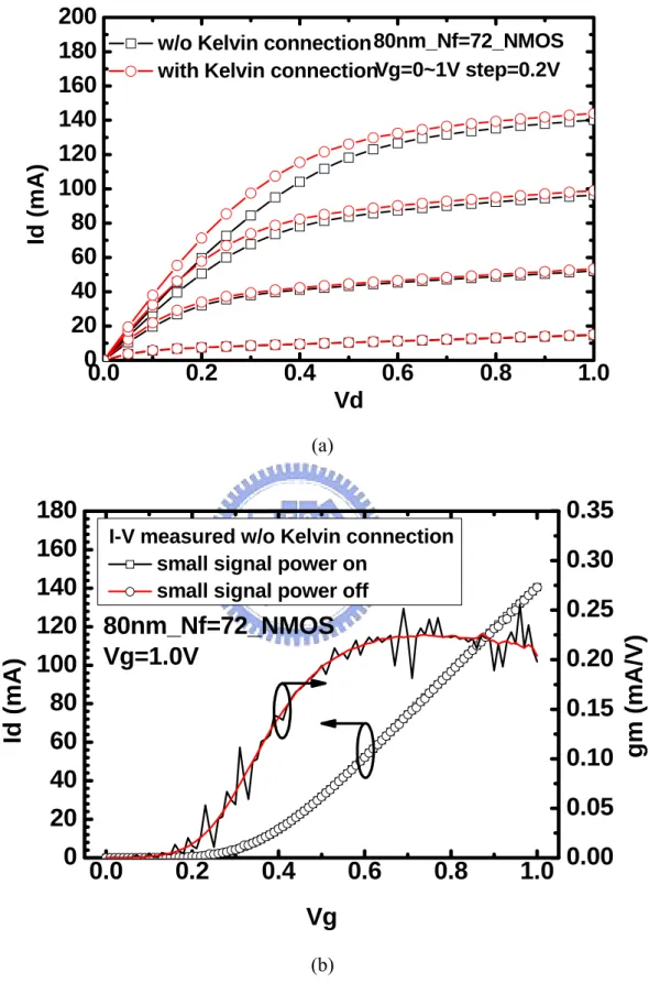
(49) Substrate current induced body effect (SCBE). It is assumed that most of the I-V and C-V parameters were fairly modeled in the original model and only minor modification is needed to improve the model accuracy. Unfortunately, the assumption can barely fit 80 nm devices but absolutely is no longer valid for 65 nm devices.. 4.2 Intrinsic I-V Model For RF MOSFET, 3–terminal test structure is usually implemented with common source configuration in which source and body terminals are tied together and grounded. To measure its high frequency characteristic (both S parameter and NFmin), two sets of probing pad with G-S-G structures are implemented and connected to the gate and drain terminals. The parasitic resistances associated with MOSFET’s terminals such as Rg_ext, Rd_ext, Rs_ext, and Rb_ext contributed from the interconnection lines and probing pads will affect I-V characteristic of DUT. Extraction of these parasitic resistances should be done and added to the original intrinsic MOSFET model (BSIM3). The mentioned parasitic resistances can be extracted from the dummy short pads which is designed to de-embed the resistive and inductive parasitics of the interconnect lines and probe pads, etc. In this study, simulation was done using Agilent Advance Design System (ADS) for model verification and calibration. Based on the original model card, default simulation results of Id-Vg and Id-Vd curves were obtained. Through comparison between simulation and measurement in terms of Id-Vg and gm-Vg curves in both linear and saturation regions, significant deviation was identified for the threshold voltage (Vth), drain current (Id), gate subthreshold swing (S), etc. As for comparison of Id-Vd curves, channel length modulation (CLM) and drain induced barrier lowering (DIBL) effects were revealed. Besides, the intrinsic and extrinsic parasitic resistances, Rd_int and Rd_ext at drain terminal will affect the rising slope between linear and saturation region.. 35.
數據
+7
相關文件
Now, nearly all of the current flows through wire S since it has a much lower resistance than the light bulb. The light bulb does not glow because the current flowing through it
For the proposed algorithm, we establish its convergence properties, and also present a dual application to the SCLP, leading to an exponential multiplier method which is shown
This kind of algorithm has also been a powerful tool for solving many other optimization problems, including symmetric cone complementarity problems [15, 16, 20–22], symmetric
/** Class invariant: A Person always has a date of birth, and if the Person has a date of death, then the date of death is equal to or later than the date of birth. To be
This algorithm has been incorporated into the FASTA program package, where it has decreased the amount of memory required to calculate local alignments from O(NW ) to O(N )
To illustrate how LINDO can be used to solve a preemptive goal programming problem, let’s look at the Priceler example with our original set of priorities (HIM followed by LIP
The major testing circuit is for RF transceiver basic testing items, especially for LNA Noise Figure and LTE EVM test method implement on ATE.. The ATE testing is different from
情境感知巡檢路線即時導引機制之研製 Development of a Real-time Patrol Routing Mechanism in a Context-Aware Environment
In the proposed method we assign weightings to each piece of context information to calculate the patrolling route using an evaluation function we devise.. In the
