國 立 交 通 大 學
電子工程學系 電子研究所碩士班
碩 士 論 文
鎳鍺化物接觸之N
+
-P鍺淺接面
及接觸電阻之研究
A Study on the Nickel Germanide Contacted N
+-P
Germanium Shallow Junction and Contact Resistance
研 究 生: 施哲儒
指導教授: 崔秉鉞 教授
鎳鍺化物接觸之N
+-P鍺淺接面及接觸電阻之研究
A Study on the Nickel Germanide Contacted N
+-P
Germanium Shallow Junction and Contact Resistance
研 究 生: 施哲儒 Student: Che-Ju Shih
指導教授: 崔秉鉞 Advisor: Bing-Yue Tsui
國立交通大學
電子工程學系 電子研究所 碩士論文
A thesis
Submitted to Department of Electronics Engineering and Institute of
Electronics
College of Electrical and Computer Engineering
National Chiao Tung University
in Partial Fulfillment of the Requirements
for the Degree of Master of Science
In
Electronics Engineering
September 2013
Hsinchu, Taiwan, Republic of China
I
鎳鍺化物接觸之N
+-P鍺淺接面
及接觸電阻之研究
研究生: 施哲儒 指導教授: 崔秉鉞
國立交通大學
電子工程學系 電子研究所碩士班
摘要
在過去幾十年內,提升矽半導體元件的特性的研究已經越來越完整。但是隨 著元件快速的微縮,以矽做為半導體材料的金氧半場效電晶體很快就會因為物理 極限的限制而越來越難繼續微縮下去。因此,當前的課題就是發展其他可能方法 來解決這個問題。鍺由於本身的較高的載子遷移率以及和矽製程有較大的相容性 而被視為能取代矽基板做為未來半導體的材料。但是 N 型參雜在鍺基板裡面會快 速地擴散,所以好的鍺淺接面特性不容易達成,此外,由於 N 型鍺與金屬界面上, 費米能階會被鎖定在接近價帶的位置,會產生很大的蕭基位能障而導致較大的接 觸組抗。本論文主要探討利用鎳鍺化物接面來形成較淺的接面,並同時降低對 N 型鍺的接觸阻抗。 由於鎳鍺化物的電阻係數較其他金屬鍺化物來的低,且形成溫度也相對較低, 所以選用鎳鍺化物當作接面金屬。此外,本論文中使用了兩種製程來研究接面特 性,其一是形成鍺化物之前打入參雜使參雜的離子堆積在界面,另一種是形成鍺 化物之後打入參雜,接著再退火使參雜離子能夠在界面離析出來。 經過形成鍺化物之前打入參雜的製程後,在濃度較高的鍺基板上植入較淺較 高濃度的參雜所形成的鎳鍺接面特性並不好,主要是因為鎳原子擴散到接面的邊 緣,造成大量的漏電流。然而在形成鎳鍺化物之前植入氟離子卻能夠有效的抑制II 鎳原子的擴散而改善漏電流。另一方面來說,若在濃度較高的鍺基板上植入較深 較低濃度的參雜,其所形成的鎳鍺接面特性較好,漏電流比前述之鎳鍺接面來的 低。但是若在形成鎳鍺化物之前植入氟離子反而增進鎳原子的擴散進而造成漏電 流增加。推測鎳原子的擴散深淺主要是靠植入的參雜濃度所產生的缺陷來決定。 但在濃度較低的鍺基板上植入較淺較高濃度的參雜所形成的鎳鍺接面都會有好 的特性,主要是因為接面深度較深而抑制鎳擴散所造成的破壞。而且就形成鎳鍺 化物跟未形成鎳鍺化物的接面來比較,形成鎳鍺化物之後的接面,其順向電流都 有明顯的增加,是因為在形成鎳鍺化物時,參雜的離子大量堆積在鎳鍺化物與鍺 基板的界面,進而降低接觸阻抗。不論是磷參雜還是砷參雜都能看見此現象。 但在只經過形成鍺化物之後打入參雜的製程後,由於離析出來的接面深度太 淺,受到鎳擴散的影響而造成大量的漏電流。因此結合以上這兩種製程,先做形 成鍺化物之前打入參雜的製程然後再打入參雜後退火,能觀察到好的鎳鍺接面特 性,且能同時提高順向電流。最後藉由量測接觸電阻來驗證此鎳鍺接面所觀察到 的電流特性。在單純經過形成鍺化物之前打入參雜的製程的接面,其接觸電阻為 2x10⁻⁵ 歐姆-平方公分 ; 而再打入參雜後退火的接面能使接觸電阻降到 2x10⁻⁶ 歐 姆-平方公分。 總而言之,與當今發表過的研究相比,本論文利用兩種使參雜堆積的製程來 達到低接觸阻抗、低接面深度、以及好的接面特性。這個結果預期能夠改善 N 型鍺基板金氧半場效電晶體的特性。
III
A Study on the Nickel Germanide Contacted N
+-P
Germanium Shallow Junction and Contact Resistance
Student: Che-Ju Shih Advisor: Bing-Yue Tsui
Department of Electronics Engineering
Institute of Electronics
National Chiao Tung University
Abstract
In the past several decades, the research on Si-based devices progresses very fast. Furthermore, the Si-based MOSFETs have been successfully scaled down to 20 nm regime. However, scaling down the devices becomes more and more difficult and reaches the physics limits soon. Therefore, developing another ways to promote the device performance is necessary. Using new semiconducting materials is a way to improve performance. Because germanium has higher mobility and process compatibility for MOSFET fabrication process, germanium is considered to replace Si as the channel material in the future. Nevertheless, the n-type dopant diffusion in germanium is fast so that it is not easy to form shallow n+/p junction, and the high Schottky barrier height at the metal/n-Ge interface causes a high contact resistance due to the Fermi level pinning near the Ge valance band at the interface between metal and germanium. Therefore, the thesis would focus on the forming of shallow n+/p-Ge junction and low resistance metal/n-Ge contact.
Because NiGe has the lowest resistivity and low temperature formation, NiGe is selected as the contact metal. The implantation before germanide (IBG) process
IV
means ion implantation is performed before germanide formation, and the implantation after germanide (IAG) process means ion implantation is performed after germanide formation.
For the IBG junctions fabricated on heavily-doped substrate, very poor junction characteristic is observed by high dose phosphorous ion implantation due to the fast diffusion of Ni by virtue of defects which are generated by ion implantation. Fluorine ion implantation before NiGe formation could effectively suppress Ni diffusion and reduce the leakage current. Moreover, better junction characteristic can be obtained by low dose ion implantation due to the less defects resulting in less Ni diffusion. However, fluorine implantation before NiGe formation would enhance the Ni diffusion to degrade junction characteristic because the fluorine ion implantation induces extra defects. Next, on the lightly-doped substrate, good junction characteristic is more easily to be obtained than on heavily-doped substrate because the deeper junction depth on lightly-doped substrate so that the Ni diffusion would not destroy the junctions. In particular, after NiGe formation, the forward current obviously increases owing to the dopant segregation at the NiGe/Ge interface. Furthermore, either phosphorous or arsenic n+/p junction would have the dopant segregation effect. The arsenic n+/p junctions have relatively low activation concentration inferred by the I-V characteristic. Finally, because the IAG junctions have poor junction characteristic due to the segregated n+ layer is too thin to maintain good n-p junction and the Ni fast diffusion induces large leakage current, the IBG+IAG process is proposed. The IBG+IAG junction could achieve shallow junction depth and raise the forward current at the same time. Furthermore, the measured contact resistance of the IBG junction is about 2x10⁻⁵-cm2 and the lowest contact resistance of IBG+IAG junction is 2x10⁻⁶ -cm2.Therefore, this thesis has formed a junction with shallower junction depth, lower leakage current, and lower
V
contact resistance in comparison with previous studies. This achievement is expected to improve the performance of Ge nMOSFETs.
VI
致謝
在研究所的日子,無論研究、學業或生活上,都能夠學到許多,在此由衷感 謝所有曾經幫助過我的人。不論是實驗上的指導或是做學問的態度,都要非常感 謝我的指導教授 崔秉鉞老師,能夠有耐心且不遺餘力的教導我,更重要的是, 老師正直且不失圓融的性格和豐富的人生經歷更是讓我學到更多,可謂「一日為 師,終生為師」。 實驗方面則感謝交大奈米中心與國家奈米元件實驗室所提供的製程機台。謝 謝實驗室的大家,感謝元宏學長有耐心地幫我切很難切的 FIB 試片,接著要感謝 嶸健學長協助我訓練機台操作以及課業上的問題,然後感謝培宇學長和我討論實 驗上遇到的問題並教導我利用不同方法去解決問題。此外,也感謝已畢業的實驗 室學長姊們,和我同一小組的銘鴻學長、子瑜學長、炫滋學姊,在我剛進實驗室 時教導我,並給予實驗上的協助。另外感謝同組的翰奇和易謹學弟,在我受挫或 者遇到困難時能一起衝一發並讓我忘卻煩惱,還要感謝崇德能陪我聊天紓解壓力, 不僅如此,也感謝璽允、國丞、雪君的相互勉勵與支持,並且帶給實驗室一個美 好的氣氛,還要感謝學弟昕翰、致弘、立偉提供生活以及實驗上的協助,在實驗 做完時能陪我吃飯聊天。 再來要感謝我的朋友,在我遇到困難時能給我支持鼓勵並互相打氣,讓我不 再困惑,勇往直前。最後感謝我的家人,有時候忙碌無法回家還特地來新竹和我 見面,也時常打電話關心問候我,讓我在研究所的生活中能更有動力,謝謝你們 !VII
Contents
Abstract (Chinese) ... I Abstract (Englisg) ... III Acknowledgements ... VI Contents ... VII List of Tables ... IX List of Figures ... X
Chapter 1 Introduction ... 1
1.1 Background of Studying Germanium ... 1
1.2 Metal and Semiconductor Contact ... 4
1.2.1 Metal Germanide ... 5
1.2.2 Fermi Level Pinning ... 6
1.2.3 Method for Fermi Level Depinning ... 7
1.3 Dopants activation in germanium ... 9
1.4 Contact Resistance ... 10
1.5 Dopant Segregation Method ... 11
1.6 Motivation ... 12
1.7 Organization ... 14
Chapter 2 Experiments ... 21
2.1 Devices Fabrications ... 21
2.1.1 IBG + IAG Junction Formation ... 21
2.1.2 Contact Resistance of IBG+IAG junctions ... 23
2.2 Material Analysis and Electrical Measurement ... 23
Chapter 3 IBG and IAG junctions ... 32
VIII
3.2 Conventional N+/P Junctions ... 33
3.3 NiGe on Conventional N+/P Junctions (IBG junctions) ... 35
3.4 NiGe Dopant Segregation Junctions ... 39
3.5 Contact resistance of IBG+IAG junctions ... 39
3.6 Summary of IBG and IAG junctions ... 41
Chapter 4 Conclusions and Future Works ... 66
4.1 Conclusions ... 66
4.2 Future Works ... 68
IX
List of Tables
Chapter 1
Table 1-1 Interface trap density (Dit) and effective oxide thickness (EOT) recorded
by previous studies in Ge capacitor. ... 15
Table 1-2 Metal/n-Ge contact resistance recorded by previous studies. ... 16
Chapter 2 Table 2-1 Main process recipe of conventional junctions. ... 25
Table 2-2 Main process recipe of IBG junctions. ... 25
Table 2-3 Main process recipe of IAG junctions. ... 26
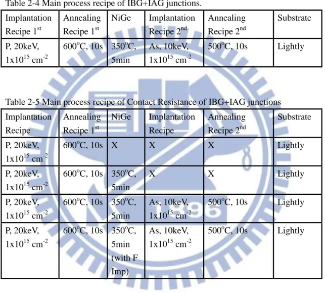
Table 2-4 Main process recipe of IBG+IAG junctions. ... 26
Table 2-5 Main process recipe of Contact Resistance of IBG+IAG junctions ... 26
Chapter 3 Table 3-1 Correction factor of samples with different shape or size[80]. ... 43
X
List of Figures
Chapter 1
Fig. 1-1 Components of the resistance associated with the source/drain junctions of a MOS transistor [64]. ... 17 Fig. 1-2 Relative contribution from each component of the resistance to series resistance for different technology nodes [65]. ... 18 Fig. 1-3 Extraction of the front resistance (Rf) from the Rtotal-Ld plot. ... 19
Fig. 1-4 Four-terminal Cross Bridge Kelvin Resistor structure with geometry parameters definition [77]. ... 20
Chapter 2
Fig. 2-1 Process flow of IBG+IAG junctions. ... 28 Fig. 2-2 Process flow of Contact Resistance of IBG+IAG junctions. ... 30 Fig. 2-3 Scheme of six-terminal Cross Bridge Kelvin Resistor structure. ... 31
Chapter 3
Fig. 3-1 Sheet resistance as a function of annealing temperatures for 5 minutes of NiGe formation. ... 45 Fig. 3-2 Sheet resistance as a function of annealing times at 350oC of NiGe formation. ... 46 Fig. 3-3 X-ray diffraction spectrum of the NiGe/Ge structure formed by 350C annealing shows polycrystal NiGe phases. ... 47 Fig. 3-4 Current-voltage curve of conventional junctions of implantation by phosphorus at 20keV to a dose of 1x1015 cm-2 and 50keV to a dose of 5x1013 cm-2 and activation at 600oC for 60 seconds on heavily-doped substrate. ... 48 Fig. 3-5 Current-voltage curve of conventional junctions of implantation by phosphorus at 50keV to a dose of 1x10¹⁵, 5x10¹³, 1x10¹³, 5x1012 cm-2 and
XI
activation at 600oC for 60 seconds in lightly-doped substrate. ... 49 Fig. 3-6 Current-voltage of conventional junctions of implantation by arsenic at 30keV to a dose of 1x10¹⁵, 5x10¹³, 1x1013 cm-2 and activation at 600oC for 60 seconds in lightly-doped substrate. ... 50 Fig. 3-7 Current-voltage curves of IBG junctions forming with different formation temperature of implantation by phosphorus at 20keV to a dose of 1x1015 cm-2 and activation at 600oC for 60 seconds on heavily-doped substrate. ... 51 Fig. 3-8 Diffusivity of elements in Ge [78]. ... 52 Fig. 3-9 Current-voltage curves of fluorine implantation before NiGe formation and IBG junctions with different formation temperature of implantation by phosphorus at 20keV to a dose of 1x1015 cm-2 and activation at 600oC for 60 seconds in heavily-doped substrate. The fluorine implantation is at 10keV to a dose of 1x1015 cm-2. ... 53 Fig. 3-10 Current-voltage curves of fluorine implantation before NiGe formation and IBG junctions with different formation temperature implantation by phosphorus at 50keV to a dose of 5x1013 cm-2 and activation at 600oC for 60 seconds in heavily-doped substrate. The fluorine implantation is at 10keV to a dose of 1x1015 cm-2. ... 54 Fig. 3-11 Current-voltage curve of IBG junctions of implantation by phosphorus at 50keV to a dose of 1x10¹⁵, 5x10¹³, 1x10¹³, 5x1012 cm-2 and activation at 600oC for 60 seconds in lightly-doped substrate. ... 55 Fig. 3-12 Total energy of the interfacial structure as a function of the dopant position. One of the Ge atoms is replaced by (a) P atom and (b) As atom. ... 57 Fig. 3-13 Current-voltage curves of IBG junctions forming with implantation by
XII
arsenic at 30keV to different dose and activation at 600oC for 60 seconds on lightly-doped substrate. ... 58 Fig. 3-14 Current-voltage curves of IAG junctions with implantation by arsenic at 10keV to a dose of 1x1015 cm-2 with different annealing temperature. ... 59 Fig. 3-15 Cross-sectional TEM micrography of the NiGe/Ge structure with IAG process after annealing at (a) 500C and (b) 550C for 10 sec. ... 60 Fig. 3-16 Current-voltage curve of IBG (phosphorus at 20keV to a dose of 1x10¹⁵
cm-2 and activation at 600oC for 10 seconds) + IAG(arsenic at 10keV to a dose of 1x1015 cm-2) junction with 500C for 10 seconds annealing. ... 61 Fig. 3-17 Cumulative distribution of contact resistivity extracted by the CBKR structure. The contact areas are 10x10, 5x5 and 3x3 um2. ... 62 Fig. 3-18 Secondary ion mass spectrometer depth profiles of the conventional junction of implantation by phosphorus at 20keV to a dose of 1x1015 cm-2 and activation at 600oC for 10 seconds on lightly-doped substrate. ... 63 Fig. 3-19 Secondary ion mass spectrometer depth profiles of the NiGe-contacted junction formed by the IBG process of implantation by phosphorus at 20keV to a dose of 1x1015 cm-2 and activation at 600oC for 10 seconds on lightly-doped substrate. ... 64 Fig. 3-20 Secondary ion mass spectrometer depth profiles of the NiGe-contacted junction formed by the IBG (implantation by phosphorus at 20keV to a dose of 1x1015 cm-2 and activation at 600oC for 10 seconds) + IAG (implantation by arsenic at 10keV to a dose of 1x1015 cm-2 and annealing at 500C and 10 seconds). ... 65
Chapter 4
Fig. 4-1 Cross-sectional TEM micrography of the NiGe/Ge structure at the junction edge. ... 70
1
Chapter 1
Introduction
1.1 Background of Studying Germanium
Germanium is one of the semiconducting materials in all elements. In particular, germanium is the material used to fabricate the first transistor in the world. It can be traced back to 1947, John Bardeen and Walter Brattain succeeded in inventing first transistor using bulk germanium in Bell Laboratories, and they were awarded the Nobel Prize in Physics with William Shockley in 1956. After that moment, germanium had become the principal material for solid-state devices from the 1950s to the early 1960s. However, as the development of Silicon, another semiconducting material, is gradually mature, silicon quickly replaced germanium to be the predominant semiconducting material from the late 1960s. One of the reasons for this evolution is that the wider band gap of silicon (~1.12eV) leads to lower leakage current in comparison with germanium (~0.67eV) [1]. Another reason is that silicon dioxide is physically and chemically stable but germanium oxide is water-soluble [1] so that silicon dioxide is more appropriate to form device isolation. The other reason is the low cost of silicon than germanium. For these reasons, silicon is generally used to fabricate semiconductor devices from the 1970s to the present [1].
In the past several decades, the development of semiconductor industry follows Moore’s law which indicates that the number of transistors on integrated circuits doubles approximately every two years [2]. At first, the gate dielectric of silicon dioxide is replaced by high dielectric constant oxide like HfO2. By applying
2
thicker than the thickness of silicon dioxide resulting in lower gate leakage current. Secondly, source and drain silicidation can lower the parasitic resistance and enhance the driving current. Therefore, the research of applying high-k materials and silicidation process has been conducted for many years. However, scaling down the devices becomes more and more difficult and reaches the physics limits soon. Therefore, developing another ways to promote the device performance is necessary. Using new semiconducting materials is the way to improve performance. Because germanium has the higher electron and hole mobility (μe=3900 and μh=1900
cm2 V-1s-1) compared with silicon (μe=1400 and μh=450 cm2 V-1s-1), germanium is
considered to be a potential channel material in the next generation [1]. Consequently, conducting complete research of germanium MOSFET is important and it is anticipated that germanium can replace silicon to improve the device performance in the future.
Although germanium has higher mobility and process compatibility for MOSFET fabrication process, some problems are still inevitable. First of all, germanium lacks suitable clean process. RCA clean is a standard clean process for silicon. However, germanium is not suited to RCA clean because germanium oxidized fast and the germanium oxide is water-soluble so that germanium would be consumed fast in the RCA clean process. In general, HF/H2O and HCl/H2O are used in
germanium clean process because germanium would hardly be etched by these solutions [1]. Secondly, the small band gap of germanium would induce higher junction leakage current and gate induced drain leakage (GIDL) current. Third, very high density of surface states (Dit) exists at the interface between gate dielectric and
germanium substrate [3-5]. These surface states would induce severe Coulomb scattering and decrease the electron/hole mobility. In addition, the unstable germanium oxide is also a cause of surface states [6-8]. Furthermore, n-type dopants
3
diffuse fast in germanium [9-13] and the metal/n-Ge contact exhibits high contact resistance due to Fermi level pinning effect [14-16]. Dopants in germanium actually have low solid-state solubility resulting in low doping concentration [17]. For n-type dopant, the dopant diffusion is fast so that it is not easy to form shallow n+/p junction, on the contrary, p-type dopants hardly diffuse at high temperature in germanium [18, 19]. Besides, in order to reduce parasitic resistance, metal germanide is used to form source/drain contact. However, the Fermi level is strongly pinned near the Ge valance band at the interface between metal and germanium, so the high Schottky barrier height of metal/n-Ge causes a high contact resistance.
In summary, despite the advantage of high carrier mobility in germanium, there is still some research need to be conducted for germanium MOSFET. In addition, NMOSFET has confronted more difficulties than PMOSFET [20, 21], so how to improve the germanium NMOSFET is of the first importance. To the present, some research has been conducted to reduce the surface states at the gate oxide and germanium interface, for example, germanium oxidation before gate dielectric deposition [22] and plasma recovery of interface states [23]. Furthermore, the effective oxide thickness (EOT) is also reduced to lower than 1 nm by depositing different high-k materials [24]. Table 1-1 lists the Dit and EOT reported in some
literatures. On the other hand, the researches about the n+/p-Ge shallow junction and the contact resistance of metal/n-Ge contact are not complete [25-27]. Therefore, the thesis would focus on the forming shallow n+/p-Ge junction and low resistance metal/n-Ge contact.
4
1.2 Metal and Semiconductor Contact
When metal contacts with semiconductor, either Schottky contact or ohmic contact forms. The metal work function (φm) is defined as the energy difference
between vacuum level and Fermi level of metal; the semiconductor work function (φs)
is defined as the energy difference between vacuum level and Fermi level of semiconductor, and χ is electron affinity. As soon as the metal and semiconductor contact intimately, according to the Einstein relation, the Fermi levels should be connected horizontally and continuous in electrostatic equilibrium. Whether it is a Schottky contact or ohmic contact is decided by the work function difference and dopants type of semiconductor. Take metal/n-type Si as an example; in the case of φm
> φs, the Fermi level of semiconductor is higher than the Fermi level of metal. It
means that the electrons in semiconductor near the interface would diffuse to metal after the two Fermi levels are aligned so that a potential barrier and a depletion region would be formed near the junction. Therefore, the Schottky barrier height can be expressed as φbn=φm –χ. It is called a Schottky contact or rectifying contact. However,
in the condition of φm < φs, the Fermi level of semiconductor is lower than the Fermi
level of metal. After the two Fermi levels are aligned, the barrier between metal and semiconductor is small and the barrier is easily overcome by a small electrostatic potential energy. It is called an ohmic contact.
Schottky contact is like a rectifying junction and ohmic contact can be regarded as a very small resistor. What kind of contact should be formed is based on the purpose of the device. Furthermore, whether it is Schottky contact or ohmic contact can be controlled by the work function difference and the dopants type of semiconductor.
5
1.2.1 Metal Germanide
In 1966, silicide formation was first confirmed to be practical to form ohmic and Schottky contact. Because of high melting point, high thermal stability, and low resistivity, silicide has been widely used in the state-of-the–art VLSI process technology. In order to reduce the parasitic resistance, self-aligned metal silicide (salicide) process was introduced in 1981 [28-30]. Salicide is the process that sputtering a metal film after the gate and source/drain diffusion region formation, then annealing by rapid thermal annealing (RTA) to let metal reacts with silicon to form metal silicide. After silicide formation, selected wet etching is used to remove unreacted metal. By the salicide process, silicide is only formed on the silicon exposed regions. In brief, salicide has plenty of advantages not only reducing parasitic resistance and contact resistance but also the self-aligned feature.
In germanium devices, germanide is also used for the purpose similar to the silicide in silicon devices. In the germanidation process, the germanide must have the following characteristics: low resistivity, less germanium consumption, and good thermal stability. There were many kinds of metals have been examined for germanidation such as Fe, Co, Ni, Pd, Pt, and Cu [31]. Among them, NiGe and PdGe are considered to be the candidate due to the lower resistivity, but nickel is the most appropriate metal to form germanide for four reasons. At first, NiGe has the lowest resistivity (< 22 μΩ.cm) [31-33]. Secondly, NiGe forms at low temperature [34]. Some research showed that NiGe can be formed at 275oC. Third, unreacted nickel can be easily removed by HCl or hot H3PO4 [35].Lastly, it is thermodynamically stable
with no Ge-rich phase nickel germanide [31, 36, 37]. Furthermore, nickel controls the diffusion in germanidation, and Ni2Ge forms in the beginning then transit to NiGe.
6
has two disadvantages in application. One of the disadvantages is germanium out diffusion during germanidation [38]. Research showed that germanide overgrows over the SiO2 isolation by one-step formation (330oC) and germanium voids left around the
corner of isolation, but no overgrowth appears by two-step formation process (270oC/330oC). In addition, a method has been proposed to solve this problem, oxidation to form thin GeO2 between nickel and germanium before germanidation
[39], but whether it is effective is necessary to be proved. The other disadvantage is that NiGe is thermally unstable. The sheet resistance of NiGe increases sharply above 500oC, ascribed to NiGe agglomeration [40]. When some metals are added to form germanide between nickel and germanium such as Pt [41] and Ti [42], the thermal stability could be improved.
1.2.2 Fermi Level Pinning
In ideal case, as metal contacts with semiconductor to form Schottky contact, the Schottky barrier height might changes with different kinds of metals due to different work functions following the relationship of φbn=φm–χ. However, in the
metal/germanium contact, the Schottky barrier height almost would not changes with different metals. It is just like the Fermi level is pinned at a fixed position resulting in the Schottky barrier height unchanged; this phenomenon is called the Fermi level pinning. There is a formula to express the Fermi level pinning, φbn=S(φm-φCNL)+(φCNL-χ), where φbn is Schottky barrier height, φm is metal work
function, φCNL is charge neutrality level, χ is electron affinity, and S is pinning factor.
The pinning factor can be used to judge whether Fermi level pinning exists. If S approaches to 1, it means Schottky barrier height changed with metal work function, so Fermi level pinning effect hardly exists. On the contrary, If S approaches to 0, it
7
means Schottky barrier height unchanged with metal work function. Therefore, by sketching the relation of φbn and φm,the slope gives the pinning factor S and that the
extent of Fermi level pinning is obtained.
In general, the causes of Fermi level pinning effect could be attributed to interface state. The interface state stems from Metal Induced Gap States (MIGS) [14] and dangling bonds. MIGS is the fact that when metal contacts with semiconductor, metal electron wave function would penetrate into semiconductor band gap. In addition, the other cause is the dangling bonds existing at semiconductor surface. However, the research of Fermi level depinning by insertion of a dielectric layer [43] or a doping segregation layer [44] would not completely support these two causes of Fermi level pinning, so the reasons of Fermi level pinning is not quite clear now. Charge neutrality level (CNL)[45] then comes into existence by virtue of surface states interaction. Furthermore, Fermi level is usually pinned at the charge neutrality level. For germanium, the Fermi level is pinned at 0.1eV above the valence band and the pinning factor S = 0.05 [16]. As a result, the metal/n-germanium Schottky barrier height is high.
1.2.3 Method for Fermi Level Depinning
Due to the Fermi level pinning effect mentioned above, the barrier height between metal and semiconductor could not change with metal work function. In addition, Fermi level is always pinned at near valence band on germanium so it is difficult to form ohmic contact on n-type germanium. Therefore, some methods have been presented to relax the Fermi level pining effect and/or modify the Schottky barrier height [43, 46, 47]. Surface passivation is a kind of the way by using solution immersion, ion implantation, or plasma treatment to relax the Fermi level pinning
8
effect. By these techniques, the dangling bond would be reduced by means of surface passivation so that the Fermi level pinning effect would be alleviated. Research show that (NH4)S solution immersion, sulfur implantation into germanium, and CF4 plasma
treatment can effectively alleviate Fermi level pinning [44, 47, 48]. The other method is insertion of thin dielectric film. Several researches have different idea to explain the mechanism about Fermi level depinning. Some research showed that the dipole would exist at the interface to cause shift of the pinning position [49-51] and other research indicated many fixed oxide charges in the dielectric to cause band bending [52]. In addition, there are many research discussing about Fermi level depinning by insertion of TiO2[46], Al2O3[46], Si3N4, Si[53], and Ge3N4[54]. However, insertion of dielectric
film would cause the additional tunneling resistance to reduce on-current. The tunneling resistance is determined by the thickness of dielectric and the conduction band offset (CBO) of dielectric to germanium. On the one hand, the thinner dielectric would get lower resistance but the dielectric may be not enough to block metal electron wave function penetration. Therefore, it is critical to determine the thickness of dielectric film. On the other hand, conduction band offset can also affect the tunneling resistance. For example, conduction band offset of TiO2 is nearly zero to
germanium so that there is nearly no tunneling resistance or barrier. Consequently, the thickness of TiO2 would not affect the contact resistance a lot.
In short, there are many kinds of methods for Fermi level depinning such as surface passivation and insertion of dielectric film. Furthermore, Fermi level depinning is exactly an important issue to form ohmic contact or get lower contact resistance.
9
1.3 Dopants activation in germanium
As the devices scale down generation by generation, the dimension of transistor becomes smaller and smaller and the device structure become more and more complicate as well. When the channel length decreases, short channel effect then occurs. Short channel effect is an effect that the depletion width of source/drain is too large to affect the gate threshold voltage, and it usually happens on small devices. Therefore, forming ultra-shallow junction is the best way to relax this effect. However, forming ultra-shallow n+/p-Ge junction is difficult.
In advanced CMOS process, ion implantation is the prevalent way to form source/drain doping. Nevertheless, ion implantation would produce lots of defects in the implantation region. The defects may affect device performance and enhance dopant diffusion, but high temperature annealing could recover these defects. In germanium, n-type dopants diffuse fast at high temperature [9-13] and dopants are difficult to activate to obtain high carrier concentration because of low solid-state solubility [17]. Because activation of n-type dopants needs higher than 500oC thermal annealing [55, 56] but shallow junction needs low temperature process, it is hard to form n-type high-concentration and ultra-shallow junction by ion implantation. Besides, phosphorous has lower diffusion coefficient and higher solid-state solubility than the other n-type dopants. On the contrary, p-type dopants behave totally different from n-type dopants [18]. P-type dopants have higher activation concentration (Boron: 6x1020cm-3 versus Phosphorous: 2x1020cm-3) and hardly diffuse even at high temperature [19].
In the past, many methods were raised to increase activation concentration and retard the dopant diffusion. One of the methods is using laser annealing to activate dopant, which could obtain high activation concentration because of high temperature
10
and short dopant diffusion because of transient annealing [57-59]. Another one is co-implantation, for example, antimony and phosphorous co-implantation due to local strain compensation between antimony and phosphorous [60, 61] or phosphorous and fluorine co-implantation because fluorine passivation of the defects in Ge to increase the activation concentration [62]. ;. The other one is spin-on dopant which is free from ion damage [63].
1.4 Contact Resistance
As devices scale down, the parasitic resistance becomes more and more critical for high performance devices. Parasitic resistance is composed of source/drain extension (SDE) to gate overlap resistance Rov, SDE resistance Rext, deep S/D
resistance Rdp, and silicide-diffusion contact resistance Rc as shown in Fig.1-1 [64].
Every factor would affect device performance greatly. However, for the smaller devices, the contact resistance plays the predominant role to affect the parasitic resistance as shown in Fig.1-2 [65]. Therefore, it is important to pay more attention on reducing metal/semiconductor contact resistance.
The contact resistance (Ω) issue is always discussed in another criterion, specific contact resistance (ρc) without the influence of contact size. Specific contact
resistance is defined as the reciprocal of deviation of current density to voltage at zero voltage.
𝜌𝑐 ≡ (𝜕𝑉𝜕𝐽) 𝑉=0 −1
(Ω‧cm2), where J is current density (A/ cm2) and V is voltage (V).
For the low doping concentration metal/semiconductor contact, the thermionic emission mechanism leads the current transportation. Therefore, ρc can be expressed
11 by
𝜌𝑐(𝑇𝐸) =𝑞𝐴𝑘∗𝑇exp(
𝑞𝜙𝐵
𝑘𝑇),
where k is Boltzmann constant, q is the charge of an electron, A* is Richardson constant, T is absolute temperature, and ΦB is Schottky barrier height. As a result,
reducing the Schottky barrier height could get lower specific contact resistance. Furthermore, for the high doping concentration metal/semiconductor contact, the tunneling mechanism would lead the current transportation. Therefore, ρc can be
expressed by
𝜌𝑐(𝐹𝐸) ∝ exp [2√𝜖𝑠𝑚∗
ℏ (
𝜙𝐵
√𝑁𝑑)],
where ɛs is dielectric constant, m* is electron mobility, and Nd is doping concentration.
Consequently, in order to reduce specific contact resistance, increasing the doping concentration and reducing the Schottky barrier height are necessary.
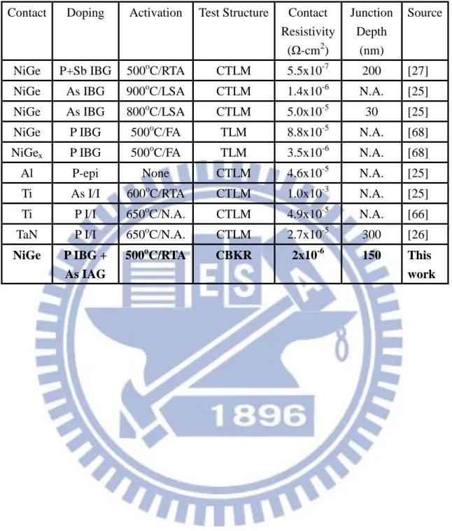
As a result, the specific contact resistance should be reduced in metal/n-Ge having Fermi-level pinning effect. In addition, there have been already some research not only increasing the doping concentration but also reducing the Schottky barrier height to reduce metal/n-Ge specific contact resistance [25, 66-70].
1.5 Dopant Segregation Method
Dopant segregation method can be used to increase doping concentration and modulate the effective Schottky barrier height in order to reduce contact resistance. The dopant segregation junction depends on very high doping concentration that leads to a strong band bending at the interface between metal and semiconductor, so the carriers could tunnel through the barrier easier. There are two kinds of ways to form the Ge dopant segregation junction, implantation after germanidation and
12
implantation before germanidation. Implantation after germanidation is the way implanting dopants into the metal germanide after metal germanide formation, then annealing at medium temperature to let the dopants diffuse out and segregate at the interface [71]. Since ion implantation is performed after germanide formation, we call it the implantation after germanidation (IAG) process. With different segregation coefficient of varied dopants, the effect of segregation would be different. On the other hand, dopant segregation is the way dopants implantation first followed by metal germanide formation. During germanidation, the dopants segregate in front of the forming germanide front because of the snowplow effect of the dopants [72]. Since the ion implantation is performed before germanide formation, we call it the implantation before germanidation (IBG) process. Research showed that sulfur and selenium could reduce effective Schottky barrier height [47, 73]. In brief, no matter what kind of processes is used to form the dopant segregation junction, the purpose is utilizing dopant segregation to form high doping concentration region at the interface. As a result, dopant segregation junction formation could change the Schottky contact with high Schottky barrier to ohmic contact for reduction of metal/Ge contact resistance.
1.6 Motivation
In order to reduce the parasitic resistance, metal germanide would be selected to form S/D contact due to its low resistivity. NiGe is selected to be the germanide due to its low resistivity and low formation temperature. In addition, because of fast diffusion of n-type dopants and low activation concentration in germanium, the general high temperature RTA activation would form a deep junction and is hard to form shallow junction. In this thesis, IBG process and IAG process are introduced to
13
form shallow junction. The doping concentration may be high due to segregation, and the junction depth may be shallow.
Moreover, because the Fermi level is pinned near the germanium valence band, the high Schottky barrier exists on the NiGe/n-Ge contact and the contact resistance would be high. On the contrary, the specific contact resistance on NiGe/p-Ge would be as low as 2x10⁻⁷ Ω‧cm2 [32]. Previous studies showed that contact resistance was reduced by laser annealing [25], which is a high temperature process, and some other papers [25, 26, 66, 68] also showed low contact resistance in Table 1-2. However, in this thesis, IBG+IAG process and dielectric insertion are introduced to get low contact resistivity without high temperature annealing. At first, the high n-type doping is formed by implantation and RTA. Secondly, NiGe formation can let the dopant segregate at the NiGe/n-Ge interface. Next, n-type dopants are implanted into the NiGe. Finally, annealing by RTA let the dopants diffuse out to segregate again. Due to the dual-segregation, high doping concentration is expected. Furthermore, the effective Schottky barrier height is also reduced because the band bending in high doping concentration causes carrier tunneling. According to ρc formula of high doping
concentration, ρc would be reduced by high doping concentration and low Schottky
barrier height.
In summary, the thesis is focused on forming shallow n+/p junction and reducing the contact resistivity by dopant segregation method and dielectric insertion method. It is anticipated to improve the performance of S/D junction on germanium NMOSFET in next generation.
14
1.7 Organization
Chapter 1 includes the introduction of germanium characteristics and the encountered problems in metal contact and n+/p-Ge junction. In addition, the contact resistance and dopant segregation method are also introduced in the chapter. Chapter 2 describes the fabrication process of samples. Material and electrical analysis are introduced as well.
Chapter 3 focused on the IBG junction. The conventional junctions of different implantation dosage are first discussed, then forming NiGe, which named IBG junction, is done to compare the electrical characteristics with conventional junctions. Furthermore, studying IBG junction on different concentration substrates and the effect of Ni diffusion is also included. Finally, the contact resistance of the IBG+IAG junctions are also showed, the results are proved by material analysis as well.
Finally, Chapter 4 summarizes the experiment results and makes some conclusions. The future works are suggested as well.
15
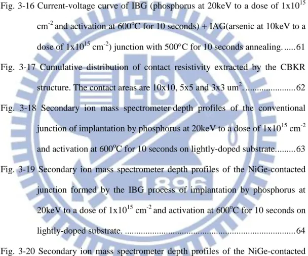
Table 1- 1 Interface trap density (Dit) and effective oxide thickness (EOT) recorded by
previous studies in Ge capacitor.
Gate stack Treatment Dit
(cm-2 eV-1)
EOT (nm)
Source
Ge/GeOx/Al2O3 O2 plasma and
PDA in N2
at 400oC, 30 min
1x10¹¹ ~1 [23]
Ge/GeOx/ Al2O3/HfO2 N.A. 5x10¹¹ 0.76 [24]
Ge/GeON/HfTiON PDA in NH3 ambient
at 500oC, 300s
2.3x10¹¹ 0.96 [74]
Ge/GeON/HfTiON PDA in wet NO
at 500oC, 300s
1.2x10¹¹ 1.02 [74]
Ge/GeON/TaON/ HfTiON PDA in wet NO
at 500oC, 40s
5.4x10¹¹ 0.91 [75]
Ge/GeON/TaON/ HfTiON PDA in NH3 ambient
at 500oC, 40s
6.8x10¹¹ 0.86 [75]
16
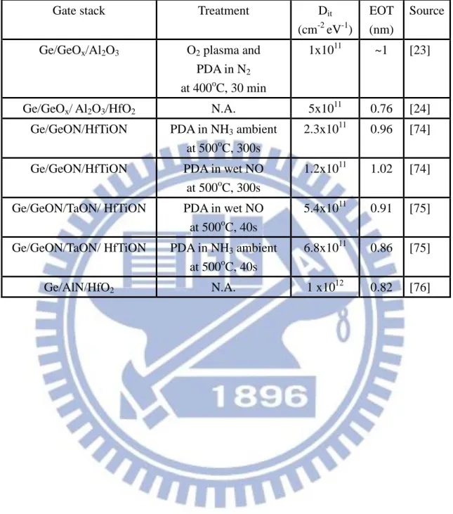
Table 1- 2 Metal/n-Ge contact resistance recorded by previous studies. Contact Doping Activation Test Structure Contact
Resistivity (Ω-cm2) Junction Depth (nm) Source
NiGe P+Sb IBG 500oC/RTA CTLM 5.5x10⁻⁷ 200 [27]
NiGe As IBG 900oC/LSA CTLM 1.4x10⁻⁶ N.A. [25]
NiGe As IBG 800oC/LSA CTLM 5.0x10⁻⁵ 30 [25]
NiGe P IBG 500oC/FA TLM 8.8x10⁻⁵ N.A. [68]
NiGex P IBG 500oC/FA TLM 3.5x10⁻⁶ N.A. [68]
Al P-epi None CTLM 4.6x10⁻⁵ N.A. [25]
Ti As I/I 600oC/RTA CTLM 1.0x10⁻³ N.A. [25]
Ti P I/I 650oC/N.A. CTLM 4.9x10⁻⁵ N.A. [66]
17
Fig.1-1 Components of the resistance associated with the source/drain junctions of a MOS transistor [64].
18
Fig.1-2 Relative contribution from each component of the resistance to series resistance for different technology nodes [65].
19
Fig.1-3 Extraction of the front resistance (Rf) from the Rtotal-Ld plot.
-2 0 2 4 6 8 0 400 800 1200 1600 2000 2400
R
to tal(
)
L
d(
m)
2R
fR
total=R
sx L
d/W
d+ 2R
fR
s=-2R
fx W
d/L
d20
Fig.1-4 Four-terminal Cross Bridge Kelvin Resistor structure with geometry parameters definition [77].
21
Chapter 2
Experiments
2.1 Devices Fabrications
In this section, the fabrication processes of devices used in this thesis are described in detail. Two kinds of Ge substrate were used. They are Ga-doped (100)-oriented Ge wafer with resistivity 0.01~0.05 ohm-cm and Ga-doped (100)-oriented Ge wafer with resistivity 1~10 ohm-cm. The former one is called heavily doped substrate and the later one is called the lightly doped substrate.
2.1.1 IBG + IAG Junction Formation
All the samples were dipped in diluted HF solution (HF:H2O=1:50) for 2
minutes and rinsed by DI water for 5 minutes to clean the surface at first. Then, 300-nm-thick Tetraethyl orthosilicate (TEOS) SiO2 was deposited by a plasma
enhanced chemical vapor deposition (PECVD) system at 350oC as field oxide. Active regions were patterned by typical lithography process and the field oxide was etched by buffered oxide etchant (BOE) for 90 seconds. The residual photo-resist was removed by acetone in ultrasonic cleaner for 1 minute.
The samples on the heavily-doped Ge substrate were implanted by Phosphorus at 20 keV to a dose of 1x1015 cm-2 and at 50keV to a dose of 5x1013 cm-2. Furthermore, the samples on the lightly-doped Ge substrate were implanted by Phosphorus at 50 keV to a dose of 1x10¹⁵, 5x10¹³, 1x10¹³, or 5x1012 cm-2 and Arsenic at 50 keV to a dose of 1x10¹⁵, 5x10¹³, or 1x1013 cm-2. All samples were annealed at 600 oC for 60
22
seconds in N2 ambient by a rapid thermal annealing (RTA) system to activate the
dopants, and the N+/P-Ge junctions formed.
Before Ni deposition, some heavily-doped samples were implanted by Fluorine at 10keV to a dose of 1x1015 cm-2 to study the effect of fluorine on the Ni diffusion. Moreover, the samples were dipped in diluted HF solution (HF:H2O=1:100) for 2
minutes and rinsed by DI water for 5 minutes to clean the surface. After that, Ni was deposited to 10-nm-thick to form germanide and TiN was deposited to 15-nm-thick to passivate Ni surface by a co-sputtering system. The Ni deposition was performed under the condition of Ar with 100 sccm and 300W at the rate about 0.5nm/sec, moreover, the TiN deposition was performed under the condition of Ar/N2 with
100/10 sccm and 800W at the rate about 0.68nm/sec. The Ni-deposited samples were annealed at 350oC for 5 minutes by a backend vacuum annealing furnace to form NiGe. The process is called IBG process.
After forming NiGe, the unreacted metal was selectively etched by hot H3PO4 at
150oC for 5 minutes and the NiGe formation is finished. Samples were implanted again by Arsenic at 10 keV to a dose of 1x1015 cm-2 and annealed at 500/550/600oC for 10 seconds in N2 ambient by rapid thermal annealing (RTA) to segregate the
dopants at the interface. The process is called IAG process.
Finally, a 300-nm-thick Al was deposited by a thermal coater to act as the contact metal. The Al layer was patterned by the typical lithography process and high density plasma - reactive ion etching (HDP-RIE) with Cl2 and BCl3 as the reacting gas, and
the residual photo-resist was removed by acetone in ultrasonic cleaner for 1 minute. A 300-nm-thick Al was deposited again by a thermal coater at wafer backside to form backside contact.
First, the conventional junctions were fabricated by the IBG process flow but skipping the NiGe related process steps and the main process conditions are
23
summarized in Table 2-1. Secondly, the IBG junctions are only fabricated by IBG process and the main process conditions are summarized in Table 2-2. Next, the IAG junctions are only fabricated by IAG process and the main process conditions are summarized in Table 2-3. Finally, the IBG+IAG junctions are fabricated by IBG and IAG process and the main process conditions are summarized in Table 2-4. In addition, the process flow of IBG+IAG junctions is depicted in Fig. 2-1.
2.1.2 Contact Resistance of IBG+IAG junctions
Lightly doped Ge substrate was used in this experiment. The process flow is identical to the IBG+IAG junction. However, after activation annealing, 300-nm-thick TEOS SiO2 was deposited again; then, contact regions were patterned and the oxide
was etched by BOE for 90 seconds. The main process conditions of the contact resistance of IBG+IAG junctions are summarized in Table 2-5. Also, the process flow is depicted in Fig. 2-2.
The contact resistance were extracted by six-terminal D-type CBKR structure shown in Fig.2-3. The contact area values of the CBKR structures used in this thesis are designed in 3x3 μm2, 5x5 μm2, and 10x10 μm2. The widths of current arms and voltage arms are designed to be the same values as the contact widths. The process tolerances are considered with 3μm.
2.2 Material Analysis and Electrical Measurement
The Current-voltage (I-V) characteristics of devices were measured by a semiconductor analyzer of model Agilent 4156C. The contact resistance was also measured by the same semiconductor analyzer. Sheet resistance was measured by a
24
four point probe system. Furthermore, the samples were analyzed by different kinds of material analysis instrument in order to compare with the results of electrical measurement, for example, X-ray Diffraction (XRD), Transmission Electron Microscopy (TEM), Scanning Electron Microscopy (SEM), and Secondary Ion Mass Spectrometer (SIMS).
XRD was used to analyze the crystallized orientation of NiGe. When X-ray goes through the crystallized structure, the constructive interference occurs. According the Bragg’s Law (nλ=2dsinθ), the constructive interference only occurs for certain θ correlating to a (h k l) plane. Therefore, the crystallized (h k l) plane of NiGe can be inferred. TEM was used to observe the microstructure of NiGe film. TEM depends on electrons beam transmitted through an ultra-thin specimen and the electrons beam interacts with the specimen as it passes through to form the image. The image is magnified and focused on the imaging device with high resolution. Therefore, the quality of NiGe film can be clearly observed. In addition, SEM is used to observe the surface of NiGe film. SEM produces images by means of scanning the samples with electrons beam and the electrons interact with atoms in the samples to detect the signal and show the samples’ surface topography. SIMS was used to analyze the distribution of elements in the samples, such as P, As, and Ni. SIMS analysis relies on sputtering the surface of the samples with a focused ion beam and analyzing the ejected secondary ions from the surface. The kind of elements could be determined by mass/charge ratios of these secondary ions. Moreover, the amount and depth distribution of the elements could also be detected at the same time.
In brief, all the material analysis plays the role of assistant to prove the measured electrical characteristics. As long as the results are consistent, the inference or conclusion would be more convinced.
25
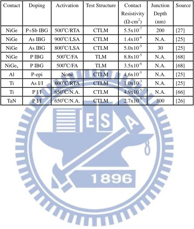
Table 2-1 Main process recipe of conventional junctions.
Implantation Recipe Annealing Recipe Substrate
P, 50keV, 5x1012 cm-2 600oC, 60s Lightly P, 50keV, 1x1013 cm-2 P, 50keV, 5x1013 cm-2 P, 50keV, 1x1015 cm-2 As, 30keV, 1x1013 cm-2 600oC, 60s Lightly As, 30keV, 5x1013 cm-2 As, 30keV, 1x1015 cm-2 P, 50keV, 5x1013 cm-2 600oC, 60s Heavily P, 50keV, 1x1015 cm-2
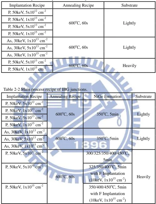
Table 2-2 Main process recipe of IBG junctions.
Implantation Recipe Annealing Recipe NiGe formation Substrate
P, 50keV, 5x1012 cm-2 600oC, 60s 350oC, 5min Lightly P, 50keV, 1x1013 cm-2 P, 50keV, 5x1013 cm-2 P, 50keV, 1x1015 cm-2 As, 30keV, 1x1013 cm-2 600oC, 60s 350oC, 5min Lightly As, 30keV, 5x1013 cm-2 As, 30keV, 1x1015 cm-2 P, 50keV, 5x1013 cm-2 600oC, 60s 300/325/350/400/450oC, 5min Heavily P, 50keV, 5x1013 cm-2 325/350/400oC, 5min with F Implantation (10keV, 1x1015 cm-2) P, 50keV, 1x1015 cm-2 350/400/450oC, 5min with F Implantation (10keV, 1x1015 cm-2)
26 Table 2-3 Main process recipe of IAG junctions.
NiGe Implantation Recipe Annealing Recipe Substrate
350oC, 5min As, 10keV, 1x1015 cm-2 500oC, 10s 550oC, 10s 600oC, 10s
Heavily
Table 2-4 Main process recipe of IBG+IAG junctions. Implantation Recipe 1st Annealing Recipe 1st NiGe Implantation Recipe 2nd Annealing Recipe 2nd Substrate P, 20keV, 1x1015 cm-2 600oC, 10s 350oC, 5min As, 10keV, 1x1015 cm-2 500oC, 10s Lightly
Table 2-5 Main process recipe of Contact Resistance of IBG+IAG junctions Implantation Recipe Annealing Recipe 1st NiGe Implantation Recipe Annealing Recipe 2nd Substrate P, 20keV, 1x1015 cm-2 600oC, 10s X X X Lightly P, 20keV, 1x1015 cm-2 600oC, 10s 350oC, 5min X X Lightly P, 20keV, 1x1015 cm-2 600oC, 10s 350oC, 5min As, 10keV, 1x1015 cm-2 500oC, 10s Lightly P, 20keV, 1x1015 cm-2 600oC, 10s 350oC, 5min (with F Imp) As, 10keV, 1x1015 cm-2 500oC, 10s Lightly
27
1. HF clean
2. 300nm SiO2 deposition
3. Active area defined by lithography process 4. SiO2 etching by BOE
5. Remove PR by ACE 6. P or As implantation 7. Dopant activation (600oC,60s) 8. Ni(10nm)/TiN(15nm) deposition by Sputter system 9. NiGe formation
10. Unreacted-Ni and TiN were etched by hot H3PO4
28 Fig.2-1 Process flow of IBG+IAG junctions.
13. Al contact defined by lithography process 14. Al etching by HDPRIE 15. Al backside contact 12. Dopant activation 11. As implantation
IAG junctions without first implantation
29
1. HF clean
2. 300nm SiO2 deposition
3. Diffusion region defined by lithography process
4. SiO2 etching by BOE
5. Remove PR by ACE 6. Implantation: P, 20keV, 1x1015 cm-2 7. Dopant activation (600oC,10s) 8. 300nm SiO2 deposition
9. Active region lithography 10. SiO2 etching by BOE
11. Remove PR by ACE 12. Ni(10nm)/TiN(15nm) deposition by Sputter system 13. NiGe formation (350oC, 5min)
14. Unreacted-Ni and TiN were etched by hot H3PO4
30
Fig.2-2 Process flow of Contact Resistance of IBG+IAG junctions. 15. Implantation : As, 10keV, 1x1015 cm-2 16. Dopant activation 17. Al contact defined by lithography process 18. Al etching by HDPRIE 19. Al backside contact
31
Fig.2-3 Schematic layout of six-terminal Cross Bridge Kelvin Resistor (CBKR) structure.
32
Chapter 3
IBG and IAG junctions
3.1 NiGe formation
In order to find out the lowest thermal budget for NiGe formation, the sheet resistance of the NiGe film formed at different thermal budgets was measured and shown in Fig.3-1 and Fig.3-2. According to Fig.3-1, the sheet resistance of NiGe decreases from 73 Ω/□ after 300 oC annealing to 20 Ω/□ after 325 oC annealing for 5 minutes and still keeps low after 400oC annealing. In addition, in Fig.3-2, the sheet resistance of NiGe decreases from 80 Ω/□ for 3 minutes annealing to 20 Ω/□ for 5 minutes annealing at 325 oC. According to the change of sheet resistance shown above, NiGe starts to growth at 325oC but the growth rate is slow so that at least a 5 minutes annealing is necessary. In the thesis, NiGe formation was performed at 350 oC for 5 minutes to ensure that NiGe could completely form if not specified. According to the formula of the sheet resistance Rsh=V/I x CF, where CF is correction factor
determined by the value of d/s, where d is the distance of the probe to the sample edge and the s is the distance between the probes, the sheet resistance of NiGe measured by the four point probe system is under the condition of infinitely large samples and the correction factor is 4.5324. However, the samples’ size used in the thesis is nearly 0.5x0.5 cm2 and the value of d/s is about 3. Therefore, the correction factor is about 2.4575 based on the Table 3-1 and the thickness of NiGe is 20 nm (Fig.3-15); then, the resistivity of NiGe is calculated to be 22.04x10⁻⁶ Ω-cm. In addition, XRD diffraction analysis on the NiGe/Ge structure formed by 350C annealing shows polycrystalline NiGe phases as shown in Fig. 3-3. The main NiGe crystal orientations
33 are (2 1 0), (1 1 2), and (1 1 1).
3.2 Conventional N
+/P Junctions
At first, the I-V curves of the conventional junctions with phosphorus ion implantation at 20 keV to a dose of 1x1015 cm-2 and 50 keV to a dose of 5x1013 cm-2 on heavily-doped substrate are shown in Fig.3-4. After dopant activation at 600 oC for 60 seconds, the junctions with phosphorus ion implantation at 20 keV to a dose of 1x1015 cm-2 has a relatively higher forward current and lower reverse current due to the higher doping concentration. The forward and reverse bias current ratio is about 5 orders of magnitude. In addition, the band-to-band tunneling can also be observed when the reverse bias exceeds 0.5 V. Because the high n+ concentration and heavily-doped substrate cause high electric field at the junction edge, the electrons would easily tunnel through the band to the other side as the reverse bias is applied.
Next, the I-V curves of conventional junctions with phosphorus ion implantation at 50 keV to different doses of 1x10¹⁵, 5x10¹³, 1x10¹³, 5x1012 cm-2 on lightly-doped substrate are shown in Fig. 3-5. After annealing at 600 oC for 60 seconds, the forward current increases with the increase of the ion implantation dose and the junction with the highest dose of 1x1015 cm-2 has the highest forward current. The reason is that more dopants could be activated to form higher concentration of n+ region so that the electron diffusion current increases and the NiGe/Ge contact resistance could be reduced. Moreover, the reverse bias current slightly increases with the increase of dose because higher ion implantation dose may induce more defects to raise leakage current. Therefore, the forward/reverse current ratio also increases with the increase of dose and the current ratio of the junction with a dose of 1x1015 cm-2 is about 103.
34
According to the depletion width formula of a p-n junction, W = [2𝜀𝑉𝑞0(𝑁1
𝑎+
1
𝑁𝑑)]
1 2
, where ε is permittivity, q is electronic charge, V0 is build-in potential, Na is
concentration of acceptor, and Nd is concentration of donor. In other words, the
depletion width is proportional to(𝑁1
𝑎+
1
𝑁𝑑)
1 2
. In addition, the reverse bias current is directly proportional to the depletion width when the generation current within the depletion region dominates the reverse bias current. Now, Na is the concentration of
substrate and Nd is the concentration of the n+ region. If the concentration of n+ region
is the same, the concentration of substrate would dominate the reverse bias current. The lower concentration of substrate would cause the wider depletion width, and the wider depletion width would cause the higher reverse bias current. Comparing the I-V curves of the conventional junctions with phosphorus ion implantation at 50 keV to a dose of 5x1013 cm-2 on lightly-doped and heavily-doped substrate, e.g. Fig.3-4 and Fig.3-5, respectively, it is the reason why the reverse bias current on lightly-doped substrate is larger than that on heavily-doped substrate.
Thirdly, the I-V curves of conventional junctions with arsenic ion implantation at 50 keV to a dose of 1x10¹⁵, 5x10¹³, 1x1013 cm-2 on lightly-doped substrate are shown in Fig. 3-6. After dopants activation at 600 oC for 60 seconds, the junction with arsenic ion implantation to a dose of 1x1015 cm-2 shows the highest forward current and the lowest reverse current; the forward/reverse current ratio is about 300. However, the junctions with dose of 5x10¹³ and 1x1013 cm-2 show poor junction characteristics. The reason is that the doping concentration is not high enough so that the arsenic doped layer is depleted.
Comparing the I-V curves of conventional junctions of implantation by phosphorus and arsenic at 50 keV to a dose of 5x1013 cm-2 on lightly-doped substrate, the reverse bias current of the arsenic implanted junction is higher than that of the
35
phosphorus implanted junction because the activation ratio of arsenic is relatively lower than that of phosphorus so that the junction depth of the arsenic implanted junction is inferred to be shallower. Furthermore, the heavier arsenic atom would generate more defects than the lighter phosphorous atom. Therefore, the reverse bias current of the arsenic implanted junction is higher as shown in Fig. 3-5 and Fig. 3-6.
3.3 NiGe on Conventional N
+/P Junctions (IBG junctions)
In this session, we examine the effect of NiGe formation on the preformed N+/P junctions, i.e the IBG junctions. Fig.3-7 shows the I-V curves of the IBG junctions with different NiGe formation temperatures. The preformed junction is implanted by phosphorus at 20 keV to a dose of 1x1015 cm-2 on heavily-doped substrate. All junctions show high reverse bias current and the electrical characteristics are nearly ohmic behavior. The junction with NiGe formation at 300oC for 5 minutes shows lower current and slightly rectifying characteristic due to incomplete NiGe formation. From Fig.3-1, the sheet resistance is higher than 70 Ω/□ which implies that Ni2Ge
formed but not NiGe formed. Other junctions have the same high forward current about 102 A/ cm2 as a result of complete NiGe formation.
Compared with the conventional junctions, before the NiGe formation, the reverse bias current is about 10-4 A/ cm2; however, the reverse bias current rises apparently after NiGe formation and the current increases with the increase of the NiGe formation temperature. It means NiGe formation causes something happened to destroy the preformed junction. According to the temperature dependence, a possible reason may be the fast diffusion of Ni. Fig. 3-8 shows the diffusivity of elements in Ge, Ni has the second high diffusivity among these elements [78]. If Ni atoms enter the depletion region of the junction, they act as generation-recombination center and
36
destroy the junction. Therefore, finding some methods to suppress Ni diffusion is important.
A method of fluorine implantation before silicide formation had been proposed to solve the problem of large leakage current caused by Ni diffusion [79]. Hence, fluorine implantation before NiGe formation was performed in this thesis in order to solve the Ni diffusion problem. Fig.3-9 shows the I-V curves of the fluorine implanted junctions with different NiGe formation temperatures. The preformed conventional junction is formed by phosphorus ion implantation at 20 keV to a dose of 1x1015 cm-2 on heavily-doped substrate. It is observed that fluorine ion implantation reduces both forward current and reverse current. This result confirms that fluorine implantation could suppress the Ni diffusion but affect the NiGe formation at the same time. The reverse bias current of the junction with NiGe formation at 325 oC is reduced by nearly 3 orders of magnitude. But the reverse bias current still increases with the increase of the NiGe formation temperature.
The junctions with deeper junction depth were fabricated to examine whether the fast diffusion of Ni still damages the junction characteristic. The deep junction was formed by phosphorus ion implantation at 50 keV to a dose of 5x1013 cm-2 on heavily-doped substrate. The I-V curves are shown in Fig. 3-10. The forward current is about 102 A/ cm2 and is nearly the same with the forward current of the IBG junctions. Furthermore, the reverse bias current is nearly 10-2 A/ cm2 and is lower than that of the IBG junction with phosphorus ion implantation at 20 keV to a dose of 1x1015 cm-2. It could be inferred that high ion implantation dose may cause more defects than low ion implantation dose does, and more defects may let Ni diffuse faster so that the reverse bias current increases. Fig.3-10 also shows the I-V curves of the IBG junctions with fluorine ion implantation. In particular, the reverse bias current of the fluorine implanted junction is higher than that of the junction without fluorine
37
implantation and also increases with the increase of the NiGe formation temperature. It could be inferred that fluorine implantation causes additional defects than phosphorous implantation and these defects enhance Ni diffusion.
Next, the IBG junctions are also fabricated on lightly-doped substrate to observe whether the junction is still destroyed by Ni diffusion. Because different implantation doses might induce different amount of defects, the IBG junctions with different implantation doses were designed to observe the effect of Ni diffusion. Fig.3-11 shows the IBG junctions formed with phosphorus implantation at 20 keV to different doses on lightly-doped substrate. The forward current of the four IBG junctions increases with the increase of the ion implantation dose due to the different activated concentrations. However, the reverse bias current of the four IBG junctions are all about 10-1 A/cm2 and do not increase with the ion implantation dose. This observation is not consistent with the IBG junctions on heavily-doped substrate. The cause could be inferred that the junction depth on lightly-doped substrate is deeper than that on heavily-doped substrate with the same ion implantation and activation conditions. The Ni diffusion is deep enough to destroy the IBG junction on heavily-doped substrate, but it is not deep enough to destroy the IBG junction on lightly-doped substrate. In addition, the forward current increases after NiGe formation due to the dopant segregation at the NiGe/Ge interface in comparison with Fig.3-5.
First-principle calculations were introduced to discuss the behaviors of the n-type dopant around the NiGe/Ge interface [81]. First, the realistic polycrystalline phases NiGe/Ge contact is built by including NiGe(112) phase only, so the NiGe/Ge contact is simulated by a supercell connecting 8 NiGe(112) layers, 16 Ge(001) layers, and 12Å -vacuum where the dangling bonds of the Ge surface are saturated by H atoms. Before exploring whether the n-type dopant such as P and As can be segregated and pile-up at the NiGe/Ge interface or not, the implanted dopant is assumed to be
![Fig. 1-1 Components of the resistance associated with the source/drain junctions of a MOS transistor [64]](https://thumb-ap.123doks.com/thumbv2/9libinfo/8748619.205412/12.892.135.767.333.898/fig-components-resistance-associated-source-drain-junctions-transistor.webp)