of a High Performance Permanent Magnet Synchronous Drive
with Reduced Switching Frequency and Loss
Tian-Hua Liu Chh-Jung Chen
ent of Electrical Engmeering
Taipei 106, Taiwan
paper proposes an improved ynchronous drive system. By three-phase current commands,
cy of the drive system can be
In
addition, the three-phasebalanced sinusoidal waveforms.
01 is designed to achieve high and a good load disturbance
A 16-bit microprocessor system
to execute the improved control experimental results validate the
Bin-Yen Ma Wu-Shiung Feng
Department of Electrical Engineering National Taiwan University
1, Section 4, Roosevelt Road, Taipei 106, Taiwan
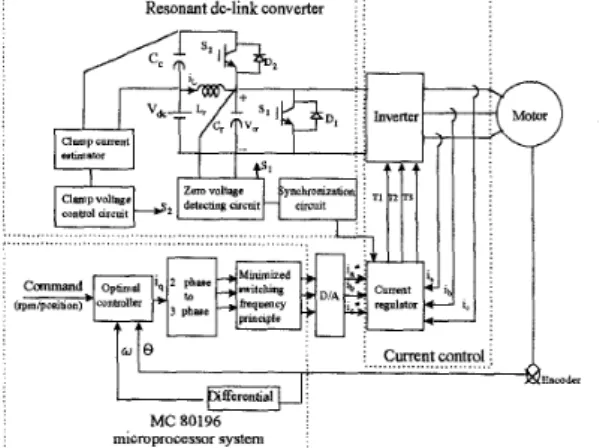
microprocessor is used to execute the optimal controller,the coordinate transformation, and the " k e d switching fiequency. The hardware circuits include a resonant dc-lmk inverter, a current regulator, feedback sensors, and a PMSM. First, the microprocessor reads the
digital
shaft position signal.Then, the microprocessor executes the d-q to a-b-c coordinate transformation. Next, the microprocessor carries out the minimized switching fiequency algorithm, and outputs the three-phase current commands
i,
, lb , andii
to the hardware circuits. The inverter is a resonant dc-link inverter. A current regulator is designed to insure that the real currents follow the current commands. The current regulator controls the inverter causing it to switch when the output voltage of the resonant dc-link converter is close to zero.A
zero voltage switching is thus obtained. The three-phase currents drive the PMSM, and a closed-loop system is achieved.In order to obtain good dynamic performance, an
optimal controller is designed. By setting a performance index, the parameters of the feedback gain can be systematically computed. Although the derivation of the control law is complicated, it is easily implemented by the microprocessor. In addition, the " k e d switching itequency method is proposed here to reduce the switchmg frequency of the inverter. Tlus minimized
* .*
Resonant dc-link converter
... : 1 1 1 1 1 1 1 : I
: ... j Currentcontrol: E n L W k MC 80196
microprocessor system
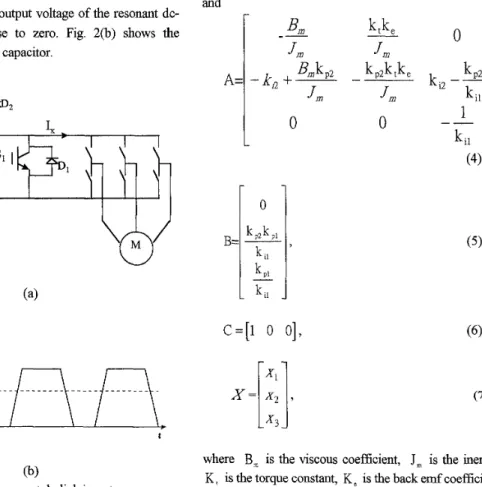
111. RESONANT DC-LINK INVERTER The resonant dc-link inverter circuit is shown in Fig. 2(a). The circuit consists of two major parts: a resonant dc-link converter and an inverter. The resonant dc-link converter, which is shown in Fig. 2(a), is composed of a resonant LC circuit, a zero voltage detecting circuit, a synchronization circuit, a clamp current estimator, and a clamp voltage control circuit [5]-[6] First, a zero voltage detecting circuit is designed to detect the instant when the resonant converter reaches zero voltage. Then, the switch
s,
is shorted to give the inductance enough energy. After the switchs,
is opened, theLC
circuit resonates. As the voltage of the resonant capacitor increases and reaches the setting clamp voltage, the clamp switchs,
is closed. Then, the energy is pumped into the clamp capacitorc,
and the voltage of the resonant capacitor is clamped. The clamp current estimator is designed to estimate the current of the clamp circuit. By suitably cont ro hg the clamp switchS,
, the energy flowing into and out the clamp capacitorC,
is balanced. The synchronization circuit is used to switch the inverter whtle the output voltage of the resonant dc- link converter is close to zero. Fig. 2(b) shows the voltage of the resonant capacitor.1,
O D 1
h
h
h
IV. OPTIMAL CONTROLLER DESIGN The optimal controller is designed by setting a performance index I as (1) 1
2
I=
-!
:
(XT
( t ) QX( t )+UT
( t ) R,U(t))dt ,where Q is a real semipositive matrix,
R,
is a real positive matrix, X is the state variable, and U is thecontrol input. If Q is selected as a matrix with larger values, then the responses are more important than the input energy. On the other hand, if
R,
is selected as a matrix with Iarger values, then the energy becomes more important.The equivalent system, whch consists of a shaping filter,
a
speed-loop controller, and a brushless motor, can be expressed as:= AX(t)
+
BU(t) , ( 2 )Y ( t ) = C X ( t ) , (3)
where A, B, C are the parameters of the equivalent system, and Y(t) is the output of the system.
and
1
--
0
ki1 (4)C = [ l
0
01,
( 6 ) t (b)Fig. 2 The resonant dc-link inverter (a)circuit (b)output voltage.
where
B,
is the viscous coefficient,J,
is the inertia,K
is the torque constant,K,
is the back emfcoefficient,K d2 , K 12 are the parameters of the speed-loop controller,
K
il , K pl are the parameters of the shaping ate r , andx,
,variables. The red system should (8) (9)
i
JU(t)l<
U,
9 I W ) l SXm,
Then from equa ons (1) and (2), we can derive the optimal control in1 ut
U*
(t) as follows:U'(t)=-K,, I .(t)+
L,,
E ,
K,,
=RI-'
BT R,,,,,
L,, =-R]
E ' [ ( A - B
R~ B~
~ , ) ~ 1 - '
(10) (11)C'Q,
(12) whereK,,
is th optimal feedback gain,Lmo
is the optimal input gainE
is the reference command. TheK O
matrix is obt,I
' ed by solving the Riccati equation:and
CT
RI
C=O,
(13)which is obtained
ia
+ ib
$.i,
=0, (14)example, when electrical angle is between 0 and 60 degrees, the lower switch ofthe c-phase is conducted. When it is between 60 and 120 degrees, the upper switch of the a-phase is conducted. The othei- cases can be seen in Fig. 3. By using this method, the average switching ti-equency is reduced to about 70 %.
A B C A PU O.Oo0 0.005 0,010 0.015 0.020 0.025 at ( 4 2 I I I I O.Oo0 0.005 0.010 0.015 0.020 0.025 at (b)
Fig. 3 The fixed switching sequence (a)voltage (b)sequence.
VI. EXPERIMENTAL RESULTS
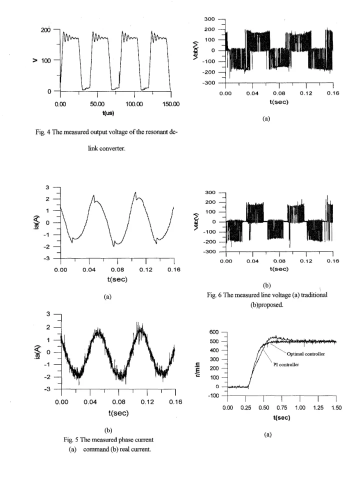
Some experimental results are shown here. Fig. 4 shows the resonant output voltage. Fig. 5 (a) shows the measured a-phase current command. Fig. 5(b) shows the measured a-phase real current. Fig. 6(a) and (b) are the measured line voltages of the traditional method and proposed method. Fig. 7(a) is the measured transient speed response. Fig. 7(b) is the measured load disturbance rejection response. Fig. 8 is the measured total efficiency of the whole system. Fig. 9 is the measured low speed response. Fig. 10 is the measured position response. The experimental results show that the
proposed system can acheve both speed control and position control with the satisfied performance.
300
7
f
-lo: -200 -300 I I I 1 1 1 1 IFig.
4
The measured output voltage of the resonant dc-0.00 0.04 0.08 0.12 0.16
link
converter. -300-
1
1
0.00 0.04 0.08 0.12 0.16 0.00 0.04 0.08 0.12 0.16 t(sec) t(sec) (b) \Fig. 6 The measured line voltage (a) traddonal (b)proposed.
(4
3 2 600 I 500ZO
400 300 (II.-
E -I.-
-2 100 -3E
200 \ 0 -100 0.00 0.04 0.08 0.12 0.16 0.00 0.25 0.50 0.75 1.00 1.25 1.50 t(sec)t(sec)
(b>Fig. 5 The measured phase current
(a) command (b) real current.
600
::I
1
0 0.0 0 : 0 Fig. 8-
0.2 0.4 0.6 0.8 1.0 t(sec) .E 40E
e
20 0 -20 -40 0.003)
!e measured speed responses nsient (b) load disturbance.
Fig. 9 The meas
__,_
__
+.,.n ___...___... -.- ... t Optimal controller +hard switching a s o f t swithing 1.5 T(N-m) 2 2.5 : measured efficiency.v
, 1 .o 1.5 2.0 t(sec)d low speed response (20 r/min)
300
-4
,‘LI
ii
loo-1
/
0.0 0.4 0.8 1.2 1.6
tIsec)
Fig. 10 The measured position response.
VII. ACKNOWLEDGMENT
Thts research is supported by the National Science Council, under grant NSC 86-2213-E011-039.
REFERENCES
[l] S. Morimoto, M. Sanada, and Y. Takada, “Wide-
speed operation of interior permanent magnet synchronous motors with high-performance current regulator,” IEEE Trans. on Ind. Appl. , vol. 30, no. 4, pp. [2] T. Sebastian and V. Gangla, “Analysis of induced
EMF waveforms and torque ripple in a brushless permanent magnet machine,” IEEE Trans. on Ind. Appl. ,
vol. 32, no. 1, pp. 195-200, Jan./Feb. 1996.
[3] W. L. Soong, D. A. Saton, and T. J. E. Miller, “Design of a new axiUy-laminated interior permanent magnet motor,” IEEE Trans. on Ind. Appl., vol. 3 1, no. 2, pp. 358-367, Mar./ Apr. 1995.
[4] L. Xu, L. Ye, Li Zhen, and A E. Antably, “A new design concept of permanent magnet machine for flux weakening operation,” IEEE Trans. on Ind. Appl., vol. 31, no. 2, pp. 373-378, Mar./Apr. 1995.
[5] D. M. Divan,“The dc resopant link converter -a new concept in static power conversion,” IIEEE Trans. Ind. Appl., vol. 25, no. 2, pp. 317-325, Mar./Apor. 1989.
[6]