Electroluminescence from metal/oxide/strained-Si tunneling diodes
M. H. Liao
Department of Electrical Engineering and Graduate Institute of Electro-Optical Engineering, National Taiwan University, Taipei, Taiwan, Republic of China
M.-J. Chen
Department of Material Science and Engineering, National Taiwan University, Taipei, Taiwan, Republic of China
T. C. Chen and P.-L. Wang
Department of Electrical Engineering and Graduate Institute of Electronic Engineering, National Taiwan University, Taipei, Taiwan, Republic of China
C. W. Liua兲
Department of Electrical Engineering, Graduate Institute of Electro-Optical Engineering, and Graduate Institute of Electronic Engineering, National Taiwan University, Taipei, Taiwan, Republic of China
共Received 20 October 2004; accepted 14 April 2005; published online 24 May 2005兲
The metal-oxide-silicon light-emitting diode under biaxial tensile mechanical strain is studied. The emission line shape of the device can be fitted by the electron-hole-plasma recombination model. The energy gap of strained Si extracted by the light emission spectra at the temperature of 120 K is reduced by 15 meV under 0.13% biaxial tensile strain. The light intensity of the device under 0.13% biaxial tensile strain increases 9% as compared to the relaxed-Si device. The upshift of valence band edge under mechanical strain to increase the majority hole concentration at the oxide/ Si interface may be responsible for this light emission enhancement. The mechanical strain is measured by Raman spectroscopy, strain gauge, and analyzed by the finite element method. © 2005 American
Institute of Physics. 关DOI: 10.1063/1.1937989兴
Strained Si attracts a great attention recently due to the enhancement of carrier mobility. The substrate strain tech-nology using the lattice misfit between Si and SiGe can yield global biaxial strain,1,2 but the high cost and high defect density make the substrate strain technology difficult for pro-duction. The biaxial strain also suffers the small hole mobil-ity enhancement at high field.3 The process-induced strain4 and package strain5can give the strain large enough for mo-bility enhancement with the low cost. The process-induced strain technology has been used in the 90 nm technology node. The strain in Si not only changes the carrier mobility but also changes the band gap and band edges due to the deformation potential.6,7 The band-gap shrinkage of Ge un-der the tensile strain was reported recently8,9 based on ab-sorption measurement which probes relatively thick sample. No luminescence results are reported for strained Si or Ge. In this letter, we report the electroluminescence 共EL兲 from strained-Si using metal-oxide-silicon 共MOS兲 tunneling di-ode. The radiative recombination of the electron-hole plasma at the accumulation layer of MOS diode can probe the band-gap reduction of Si under strain. Note that the EL is origi-nated at the very thin accumulation layer on the order of nanometer, and can probe the local strain effect, while pho-toluminescence 共PL兲 is originated from the bulk Si and probes the average strain effect within the absorption length of excitation wavelength on the order of micrometer.
The 3 nm oxide used in the MOS tunneling diode is grown by liquid phase deposition 共LPD兲 at 60 °C on 12 mm⫻12 mm p-type wafer with the resistance of
1 – 5⍀ cm. Due to the traps in LPD oxide, the trap-assistant electron tunneling is significant even with 3 nm LPD oxide. At negative bias, the electrons tunnel from the Al gate to
p-type silicon, and the holes also tunnel from p-type silicon
to Al gate. However, due to the different barrier heights be-tween electrons 共⬃3.1 eV兲 and holes 共⬃4.6 eV兲, the hole current is smaller than the electron current. Meanwhile, the negative gate bias also attracts holes in the silicon/oxide in-terface and the electrons can recombine with holes to possi-bly emit light at the accumulation layer. The thickness is measured by ellipsometry. The n-type MOS共NMOS兲 diodes have Al gate electrodes with the circular area defined by the shadow mask. Another Al contact is on the back of the wafer.
a兲Author to whom correspondence should be addressed; electronic mail:
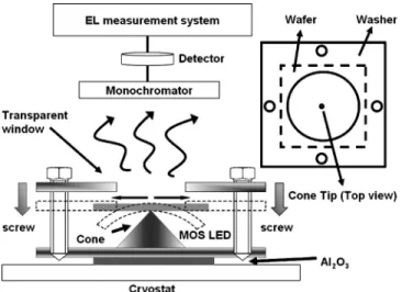
FIG. 1. Schematic diagram of the mechanical setup to apply strain in the low temperature cryostat.
APPLIED PHYSICS LETTERS 86, 223502共2005兲
0003-6951/2005/86共22兲/223502/3/$22.50 86, 223502-1 © 2005 American Institute of Physics
The experimental setup of mechanism for EL measure-ment is schematically shown in Fig. 1. The MOS light-emitting diode共LED兲 on 12 mm⫻12 mm p-type wafer sits on the tip of a cone. Then, the sample is clamped by a 20 mm⫻20 mm square washer with an inner hole of 10 mm in diameter. The level of strain is determined by the four screws on each side of the square washer. The strain of the Si under mechanical strain is simulated by finite element method共ANSYS兲, and measured by the Raman spectroscopy and strain gauge. The whole mechanism is made of copper to dissipate the heat from the electrical power. The high thermal conductivity of copper makes the temperature of MOS LED close to the cryostat temperature. Note that the whole copper mechanism has the dimension of 20 mm⫻20 mm⫻7 mm, small enough to insert into the chamber of the cryostat.
Raman spectra is excited by the laser with the wave-length of 514 nm, which has a absorption wave-length of 540 nm in Si. The Si–Si peak of silicon in the Raman spectra共Fig. 2兲 shifts towards the negative axis under the external biaxial tensile strain. The Raman shift of 0.856 and 1.02 cm−1under biaxial tensile strain were extracted from the curve fitting using Lorentzian profile, corresponding to the biaxial strain of 0.11% and 0.13%, respectively.10The strain level obtained from Raman shift agrees well with the ANSYS simulation, and has a small deviation from strain gauge measurement 共Fig. 3兲. The strain gauge measures the strain of a relatively large area 共2 mm⫻1 mm兲 on the strained Si surface. The shift of Si–Si peak for strained Si共strain=0.6%兲 on SiGe is also shown for reference.
Figure 4共a兲 shows the EL spectra at 120 K from the unstrained/strained MOS LED samples with the device size of 4⫻10−2cm2. The current used to drive the device is the
periodical pulse with the period of 30 ms and 17% duty cycle to reduce the Joule heating. The on current of the pulse is 200 mA. The electron-hole plasma recombination model is used to fit the EL spectra.11,12The band gap and device tem-perature are obtained from the fitting of the EL spectra. The energy gap extracted by the light emission spectra at the temperature of 120 K from the relaxed device is reduced by 15 meV under 0.13% biaxial tensile strain measured by Ra-man spectroscopy. Figure 4共b兲 shows the EL spectra of strained MOS LED at 120, 210, and 320 K. It is found that the EL spectrum is broadened with the increasing tempera-ture due to the wide distribution in energy of electrons and holes at high temperature. The theoretical curve and experi-mental data of Si band-gap reduction as a function of strain are also shown in the inset of Fig. 4共b兲. The strain in Fig. 4共b兲 is measured by Raman shift. It shows that the Si band gap is reduced under the biaxial tensile strain. The theoretical value of⌬Egdue to strain is calculated to be −4 meV/ Ge%
strain,13 which is close to the experimental result. Figure 5 shows integral light emission intensity as a function of biax-ial tensile strain at 300 K. Under the 0.13% biaxbiax-ial tensile strain, the light intensity from MOS LED increases 9%. It could be due to the increase of majority hole concentration at oxide/silicon interface, since the large hole concentration in-creases the radiative recombination rate of electrons and holes. The upshift of valence band edge to increase the hole tunneling barrier may be the origin to increase hole concen-tration at Si/ oxide interface. Using different parameters in Refs. 14–16 with the formula in Ref. 7, and the data in Refs.
FIG. 2. Raman spectra of the mechanical strained Si. The position of Si–Si peak of strained Si indicates 0.11%, and 0.13% biaxial tensile strain. Strained Si on Si0.8Ge0.2buffer is also shown for reference.
FIG. 3. Strain measured by Raman, strain gauge and simulated by ANSYS as a function of the number of screw turn.
FIG. 4.共a兲 Measured electroluminescence spectra of relaxed/strained MOS LED with the fitting curves of the electron-hole plasma recombination model;共b兲 EL spectra of strained MOS LED 共0.13% strain measured by Raman spectroscopy兲 at 120, 210, and 320 K. The inset of 共b兲 shows the theoretical curve共−4 meV/ %Ge strain兲 and the band-gap reduction data from EL.
223502-2 Liaoet al. Appl. Phys. Lett. 86, 223502共2005兲
17,18 the shift of valence band edge due to strain can vary from −0.8 meV/ % Ge strain to +4.5 meV/ % Ge strain, where “−” sign and “+” sign indicate the downshift and up-shift of valence band edge, respectively, and 1% Ge strain equals 0.0417% strain. The band diagram of Al/ SiO2/ p-type
Si at the accumulation condition is shown in the inset of Fig. 5. The strained LED has larger hole tunneling barriers to decrease the hole tunneling rate into the Al electrode, and more holes are accumulated at the oxide/ Si interface. With the assumption of the hole concentration increase by a factor of e⌬EV/KT due to the increase of the tunneling barrier ⌬E
V,
the⌬EVcan be obtained by fitting the intensity versus strain
curve, and the upshift of +0.7 meV/ % Ge is obtained. In our model, the hole concentration in the accumulation layer is responsible for electron-hole recombination. The doping in the Si neutral region has no effect for the recombination. As a result, the upshift of valence band edge under biaxial ten-sile strain increases the hole concentration at accumulation layer, and light emission intensity increases.
In summary, the EL from strained Si can be used to measure the band-gap reduction due to the strain. Since electron-hole plasma recombination occurs at the thin accu-mulation layer 共several nanometer from the interface兲, the local strain can be measured with the known band-gap
re-duction as a function of strain, which is approximately −4 meV/ % Ge strain. The increase of the integral emission intensity with increasing strain suggests that the valence band edge of Si shifts upwards and the hole tunneling barrier increases.
The support of Raman measurement by Professor Chih-Ta Chia at the National Taiwan Normal University is highly appreciated. This work is supported by National Sci-ence Council of ROC under Contract Nos. 93-2215-E-002-003 and 93-2215-E-002-017.
1
J. J. Welser, J. L. Hoyt, and J. F. Gibbons, IEEE Electron Device Lett. 15, 100共1994兲.
2
M. H. Lee, P. S. Chen, W.-C. Hua, C.-Y. Yu, Y. T. Tseng, S. Maikap, Y. M. Hsu, C. W. Liu, S. C. Lu, W.-Y. Hsieh, and M.-J. Tsai, Tech. Dig., Int. Electron Device Meeting, 69共2003兲
3
J. L. Hoyt, Symposium of 206th ECS Conference: SiGe: Materials,
Pro-cessing, and Devices共2004兲, 15.
4
D. Giles, M. Armstrong, C. Auth, S. M. Cea, T. Ghani, T. Hoffmann, R. Kotlyar, P. Matagne, K. Mistry, R. Nagisetty, B. Obradovic, R. Shaheed, L. Shifren, M. Stettler, S. Tyagi, X. Wang, C. Weber, and K. Zawadzki, Symp. VLSI Tech. Dig, 118共2004兲.
5
S. Maikap, M. H. Liao, F. Yuan, M. H. Lee, C. F. Huang, S. T. Chang, and C. W. Liu, Tech. Dig., Int. Electron Device Meeting,共2004兲, p. 233.
6
C. Tserbak, H. M. Polatoglou, and G. Theodorou, Phys. Rev. B 47, 7104
共1993兲. 7
C. G. Van de Walle, Phys. Rev. B 34, 5621共1986兲.
8
Y. Ishikawa, K. Wada, D. D. Cannon, J. Liu, H. C. Luan, and L. C. Kimerling, Appl. Phys. Lett. 82, 2044共2003兲.
9
J. Liu, D. D. Cannon, K. Wada, Y. Ishikawa, S. Jongthammanurak, D. T. Danielson, J. Michel, and L. C. Kimerling, Appl. Phys. Lett. 84, 660
共2004兲. 10
J. C. Tsang, P. M. Mooney, F. Dacol, and J. O. Chu, J. Appl. Phys. 75, 8098共1994兲.
11
X. Xiao, C. W. Liu, J. C. Stum, L. C. Lenchyshyn, and M. L. W. Thewalt, Appl. Phys. Lett. 60, 1720共1992兲.
12
C. W. Liu, M.-J. Chen, I. C. Lin, M. H. Lee, and C.-F. Lin, Appl. Phys. Lett. 77, 1111共2000兲.
13
R. People, IEEE J. Quantum Electron. 22, 1696共1986兲
14
EMIS Datareviews Series No. 20, Properties of Crystalline Silicon, edited by R. Hull共1999兲, p. 404.
15
C. G. Van der Walle, Phys. Rev. B 39, 1871共1989兲.
16
M. V. Fischetti and S. E. Laux, J. Appl. Phys. 80, 2234共1996兲.
17
J. J. Welser, Ph.D. thesis, Standford University, 1994.
18
S. E. Thompson, G. Sun, K. Wu, J. Lim, and T. Nishida, Tech. Dig. - Int. Electron Devices Meet.,共2004兲, p. 221.
FIG. 5. Integrated EL emission intensity vs biaxial tensile strain at 300 K. The inset shows the energy band diagram of MOS LED on p-type Si wafer at the accumulation bias. The dashed line and solid line represent the band edges of the unstrained and strained device, respectively.
223502-3 Liaoet al. Appl. Phys. Lett. 86, 223502共2005兲