q,
is copied t o the scaled differential pair M,,-M,,, yielding the required weighted voltage.Since the differential pair structure offers an extremely high input impedance, the loading effect on the controlled tran- sistor (M,,) is much r e d ~ c e d , ~ and resistance values in the MR range are readily available.
It may also be noted that the extension of this technique t o floating resistors, involving the feedback of V, and V,, would increase the quiescent power consumption and complexity, but is entirely straightforward.
Simulation results: SPICE simulations of the basic GVCR and its application as the resistive elements in the familiar two- integrator-loop biquadratic filter section have been performed. The results were obtained using realistic level 3 models (with gate-voltage-dependent mobility) for all MOS devices. However, auxiliary devices, including capacitors and oper- ational amplifiers, were assumed t o be ideal.
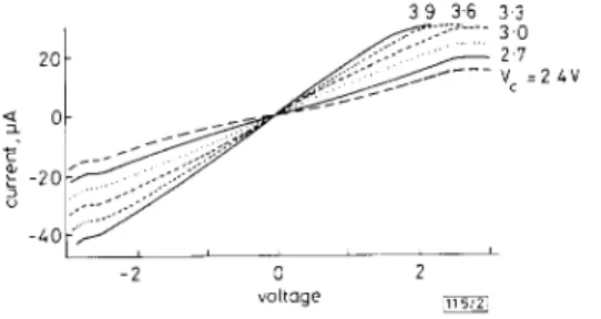
The D C current/voltage characteristics for the GVCR of Fig. 1 are shown in Fig. 2 for a range of control voltages. This family of curves shows that the resistor offers good linearity for terminal voltage swings up to 5 V,,, combined with a wide tuning range (from 60 kR t o over 200 kR for this example). It may be noted that the operational range for the gate control voltage V, is limited by the saturation conditions on MN,-M,, and Mpl-Mpz. With the bias supplies set at k 5 V it was found that V, could be varied between 2.8 and 3.9 V.
8
-- 2 0 2
voltage 1115121
Fig. 2 Variation of G V C R static vJi characteristics with control
voltage V,
As previously shown, the values for m are dependent on V,,
+,
and y and could range from 1.05 t o 1.3. In the process considered, the model parameters employed in the n-channel transistors were y = 0.65 V”’,6,
= 0.677 V and Ve = -5 V. This, it may be noted, sets m = 1.13 and requires the optimum K3/Kl, K J K , ratios t o be 3.1. However, simulation revealed that distortion was actually minimised with K J K , and K J K , at the lower value of 2.6. The discrepancies appear to be due to imperfections in the current-mirror (Mp,-Mpz) and the nonlinear nature of the differential pairs.Frequency response evaluations predict a 3 d B bandwidth
for the control circuitry of 3 MHz at I , = 6pA, a larger band- width being possible, but at the cost of increased power con- sumption and distortion. For example, doubling I , to 12pA gives a 3 dB bandwidth of 4.3 MHz, but increases distortion by 0.5%
(vi,
= 1 V,, and V, = 3.2 V).The aspect ratios resulting in minimum distortion were 5/50 for M,,-M,,, 13/50 for M,,-M,,, 70/10 for M,,-M,,, 10/50 for M,, and 8OjlO for Mpl-Mp,; V,,, was -3.8 V.
Fig. 3 shows the schematic diagram for a ‘biquad‘-type implementation of a second-order Chebyshev lowpass func-
!,to
rn
Fig. 3 GVCR-based implementation of two-integrator-loop second-
order lowpass filter structure
tion with a passband ripple of 0.5 dB and a 4 . 7 kHz cutoff frequency. Although this example contains six GVCRs, the presence of common inputs reduces the number of (identical) control circuits required (as embodied in Fig. 1) to only four.
Amplitude/frequency response simulations show good agreement with the design specification, and indicate that stopband attenuations in excess of l00dB should be attain- able at frequencies in the MHz range. Distortion analyses also show T H D levels would typically be lower than 1% for input signals up to 4Vpp.
Conclusions: A tunable grounded MOSFET resistor has been described in which linearisation is achieved via terminal- voltage feedback. Simulation results have shown that resist- ance values in the MR region can be realised, and that a biquadratic filter section based on the proposed device would maintain reasonably low levels of distortion with relatively large input signals.
These unbalanced structures could provide an economic alternative to the balanced arrangements previously advo- cated for use in fully integrated continuous-time MOSFET-C filters.
Acknowledgment: This work is supported by the National Advisory Body.
G . WILSON 23rd October 1989
P. K. CHAN
Department of Electrical & Electronic Engineering Polytechnic South W e s t
Drake Circus, Plymouth, Devon P L 4 8 A A , United Kingdom References
1 TSIDIVIS, Y., BANU, M., and KHOURY, 1.: ‘Continuous-time MOSFET-C filters’, IEEE J . Solid-state Circ., 1986, SC-21, pp.
15-29
2 BANU, M., and TSIVIDIS, Y . : ‘Floating voltage-controlled resistors in CMOS technology’, Electron. Lett., 1982, IS, pp. 678-679 3 HAN, 1. s., and PARK, s. B.: ‘Voltage-controlled linear resistor by two
MOS transistors and its application to active RC filter MOS inte-
gration’, Proc. IEEE, 1984.72, pp. 1655-1657
4 BABANEZHAD, J . N., and T E ~ , G. c.: ‘A linear NMOS depletion resistor and its application in an integrated amplifier’, IEEE J .
Solid-state Circ., 1984, SC-19, pp. 932-938
BILoTn, A.: ‘Operation of a MOS transistor as a variable tran- sistor’, Proc. IEEE, 1966,54, pp. 1093-1094
BANU, M., and TSIVIDIS, Y . : ‘Detailed analysis of nonidealities in MOS fully integrated active RC filters based on balanced net-
works’, IEE Proc. G , 1984,131, pp. 19C-196
7 TORRANCE, R. R., VISWANATHAN, T. T., and HANSON, I. v.. ‘CMOS voltage to current transducers’, IEEE Trans., 1985, CAS-32, pp. 1097-1104
5 6
CIRCUIT EXAMPLE TO DEMONSTRATE INPUTS M U S T BE CHECKPOINTS THAT FAN-OUT STEMS OF PRIMARY
Indexing terms: Logic and logic design, Logic circuits, Com- binatorial circuits
A simple circuit example is presented to demonstrate that the set of checkpoints should include the fan-out stems of primary inputs for irredundant combinational circuits. It is shown that transistor faults are not sufficient to constitute a complete set of checkpoints for combinational MOS circuits.
To reduce the time for test generation and fault simulation, the fault collapsing technique is used to reduce the number of faults to be considered. Faults are combined into classes based on a geometric structure for which the circuit is effectively divided into fan-out regions. The checkpoint theory has been presented by Bossen et al.’ and Breuer ef al.’ to collapse faults. The set of primary inputs and the fan-out branches are sufficient t o constitute a complete set of checkpoints for a
1726 ELECTRONICS LE77ERS 7th December 1989 Vol.
25
No
25combinational circuit. However, no circuit example, either in the above References or in any published literature, has been given to demonstrate that it should be necessary. As a result, many researchers, like Shih et al.,3 who dealt with this problem for MOS circuits, and Miczo? did not include the fan-out stems of primary inputs in the set of checkpoints.
In this letter we give a simple circuit example which con- tains only six NAND gates to demonstrate that the fan-out stems of primary inputs should be included in the set of check- points for irredundant combinational circuits. The logic diagram of the circuit and the circuit diagram implemented in NMOS technology are shown in Fig. la and b, respectively. Tables la and b list the stuck-at-1 and stuck-at-0 line faults of the circuit of Fig. l a and the stuck-on and stuck-open tran- sistor faults of the circuit of Fig. lb, respectively. For this circuit, the set of tests, T = {011, 101, 110, lll}, detects all single stuck-at line faults and all single transistor stuck faults of all the fan-out branches, but does not detect the primary input fanout stem fault, b stuck-at-1. To detect the b stuck-at- 1 line fault, an extra pattern {OOl} or { 100) is needed. This is because that the reconvergent fan-out of the fan-out stem 6,
:
E
d-
*
"
C e P
L/
a
Fig. 1 Example circuit ofsix N A N D gates a Logic diagram
b Circuit diagram which is implemented in NMOS technology
Table 1 FAULT TABLE FOR CIRCUIT O F FIG 1
Line stuck-at-I fault
A B C Y a b c d e f g h i J k l m n o p q
o o o o
1 1 1 1 001 0 1 1 1 1 1 1 010 0 1 1 1 1 1 1 011 1 0 0 0 0 100 0 1 1 1 1 1 1 101 0 1 1 1 1 1 1 110 1 0 0 0 0 1 1 1 1 1 111 0 -~Line stuck-at-0 fault
A B C Y a b c d e f g h I J k l m n o p q
o o o o
1 1 1 1 1 1 001 0 1 1 1 1 1 1 010 0 1 1 1 1 1 1 011 1 0 0 0 0 0 0 0 0 100 0 1 1 1 1 1 1 101 0 1 1 1 1 1 1 110 1 0 0 0 0 0 0 0 0 111 0 1 1 1 1 1 1 aTransistor stuck-on fault
ABC Y N1 N2 N3 N4 N5 N6 N7 N8 N9 N10 N11 N12 1 1
o o o o
1 1 001 0 1 010 0 1 1 1 1 011 1 0 0 0 100 0 1 1 1 1 1 101 0 1 1 110 1 0 0 0Transistor stuck-ooen fault
ABC Y N1 N2 N3 N4 N5 N6 N7 N8 N9 N10 N11 N12
o o o o
1 1 1 1 001 0 1 1 1 1 010 0 1 1 1 1 011 1 0 0 0 0 100 0 1 1 1 1 101 0 1 1 1 1 110 1 0 0 0 0 1 1 1 0 1 1 1 1 1 1 h ~~(a) Lists of line faults for circuit of Fig. l a ; and (b) lists of transistor faults for circuit of Fig. Ib. Note that only detectable faults are
listed
which is a primary input, masks this fault for T . Hence, the complete set of checkpoints must include the fan-out stem of primary inputs. It should be mentioned that this circuit is irredundant. For each fault, there exists at least one test pattern to detect it.
Fig. l a can also be implemented in the CMOS version. The same analysis can be applied.
In conclusion, this letter, for the first time, gives a circuit example to demonstrate that the fan-out stems of primary inputs are necessary checkpoints for ‘irredundant’ com- binational circuits. Breuer’s checkpoint theorem,’ therefore, should be restated as the following: ‘In an irredundant com- binational circuit, any test, which detects all single stuck faults on all primary inputs and all branches of fan-out points, detects all single faults’.
JWU-E CHEN 25th September 1989
CHUNG LEN LEE WEN ZEN SHEN Institute of Electronics National Chiao Tung University Hsin-Chu, Taiwan, Republic of China References
1 BOSSEN, 0. c., and HONG, s. I.: ‘Cause-effect analysis for multiple
fault detection in combinational networks’, IEEE Trans., 1971, C-20, pp. 1252-1275
2 BREWER, M. A., and FRIEDMAN, A. D.: ‘Diagnosis and reliable design
of digital systems’ (Computer Science Press, Woodland Hills, CA, 1976)
3 SHIH, H. c., and ABRAHAM, I. A . : ‘Fault collapsing techniques for
MOS VLSI circuits’. Proc. 16th int. symp. on fault tolerant comput., Vienna, Austria, July 1986, pp. 37&375
4 MICZO, A . : ‘Digital logic testing and simulation’ (Harper & Row,
1986), pp. 192-193
12
where
bi
is the built-in voltage (equal to the difference in Schottky barrier height&
and conduction bandgap discon- tinuity AEc), V, the pinch-off voltage, V,,, the voltage dropped in the channel at pinch-off,Km
the voltage dropped across the insulator at pinch-off and E, is the bandgap of the channel.This suggests that in a suitable high-transconductance structure it should be possible to suppress Zener tunnelling, giving reduced gate leakage. The delta-doped HIGFET,3 in which doping consists of a thin spike, has a small V,,, and thus the inequality in expr. 1 should be satisfied.
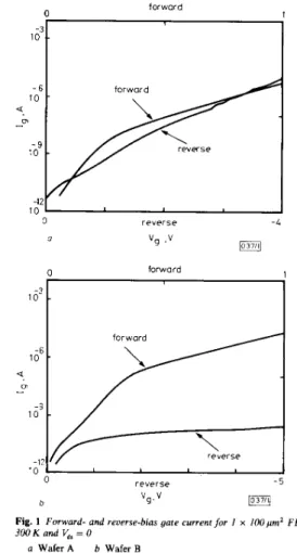
The samples used in this work were grown by MBE on Fe-doped I n P substrates. Results from two structures are dis- cussed below; these had identical insulating top layers to ensure that gate leakage associated with the insulator was the same for both wafers.
The first structure (A) consisted of a l.2pm-thick GaInAs channel ( n = 1.5 x 10’7cm-3) capped with an insulating layer of 55 nm of lattice-matched AlInAs with a 5 nm-thick layer of i-InP. The second, ‘delta-doped’, wafer (B) used a O.lpm buffer of i-InP, followed by 20nm of i-GalnAs, 6 n m of n- GaInAs ( n = 2 x 10’8cm-3) and 2 n m of i-GaInAs. The insu- lating top layers were identical t o those on structure A. Then NiAuGe ohmic contacts were annealed at 4 W C , and TiPtAu gate metal was deposited onto the i-InP antioxidation layer. FETs were mesa isolated using standard etchants.
The forward bias current is dominated by thermionic emis- sion over the channel/insulator interface. Formation of an accumulation layer leads t o nonsaturating b e h a v i o ~ r . ~
Figs. l a and b plot the gate currents for typical 1 pm gate- length FETs from wafers A and B, respectively. The forward bias gate current of both devices shows similar, i.e. non- Schottky, behaviour characterised by a sharp initial rise fol- lowed by a more gradual increase. The behaviour agrees with that predicted above.
forward
0 1
~
CONTROL OF GATE LEAKAGE I N AI In As-l N S U LATO R HIG FETs
Indexing terms: Semiconductor devices and materials, F E T s , Semiconductor doping
By proper optimisation of the channel, the gate leakage of l p m gate-length GaInAs HIGFETs has been reduced to below IOnA/mm. This has been achieved in a delta-doped structure in which Zener tunnelling is inoperative.
Ga,.,,In,.,,As (hereafter GaInAs) has many advantages when used in the conducting channel of field-effect transistors (FETs). However, one of the problems hindering the develop- ment of GaInAs-based FETs has been the low Schottky barrier height, which causes unacceptably high gate leakage. Oxidation treatments have been proposed;’ however, work on GaInAs FETs has concentrated on junction FETs,’ high elec- tron mobility transistors and heterojunction insulated gate FETs (HIGFETs).’.~
For low noise applications, the reduction of reverse bias gate leakage is of great importance. In this letter it is demon- strated that a dramatic decrease in gate leakage can be obtained by suitable design of the FET conducting channel, so that the channel is totally depleted before Zener tunnelling can become operative. This effect is observed in HIGFET devices, in which a layer of undoped high-bandgap Alo.481no.52As (hereafter AlInAs) separates the gate from the channel.
Zener tunnelling of electrons from the valence band to an empty conduction band state is much stronger in low- bandgap semiconductors like GaInAs than in GaAs. It is only operative if the voltage dropped across the channel is in excess of the bandgap. This implies that if the channel can be pinched-off by a voltage of less than its bandgap, Zener tun- nelling should be eliminated. Thus, if
E ,
>
be,
( =v,
-LS
-bi)
(1) 0 reverse -4 a v g . v n forward U reverse - 5 b vg. v1097111
Fig. 1 Forward- and reverse-bias gate current for I x 100pm’ FET at 300 K and V, = 0
a Wafer A b Wafer B
1728 ELECTRONICS LETTERS 7th December 1989 Vol 25 N o 25