IEEE JOURNAL OF SOLID-STATE CIRCUITS, VOL. 39, NO. 3, MARCH 2004 519
Brief Papers
_______________________________________________________________________________A 5-GHz CMOS Double-Quadrature Receiver Front-End With Single-Stage
Quadrature Generator
Chung-Yu Wu, Fellow, IEEE, and Chung-Yun Chou, Student Member, IEEE
Abstract—A 5-GHz CMOS double-quadrature front-end
receiver for wireless LAN application is proposed. In the receiver, a one-stage RLC phase shifter is used to generate quadrature RF signals. Implemented in 0.18 m CMOS technology, the receiver chip can achieve 50.6-dB image rejection with power dissipation of 22.4 mW at 1.8-V voltage supply.
Index Terms—CMOS technology, double-quadrature
architec-ture, IEEE 802.11a, low-noise amplifier, quadrature generator, quadrature voltage-controlled oscillator, radio frequency, receiver.
I. INTRODUCTION
W
IRELESS LANs (WLANs) provide wideband wireless connectivity between PCs and other consumer electronic devices, allowing access to core networks and other equipment in corporate, public, and home environments. The IEEE 802.11a standard [1], which refers to the 5 GHz, was defined in 1999. The physical layer of 802.11a is based on a 52 carrier orthogonal frequency division multiplexing (OFDM) modulation scheme. Theoretically, the maximum data rate can be achieved up to 54 Mb/s with 64 quadrature amplitude modulation (64-QAM).The cost of increasing the spectral efficiency according to the 802.11a standard is a strict requirement on the signal-to-noise ratio (SNR). A higher SNR results in more stringent demands on noise performance and image rejection. The specification of the 802.11a standard recommends a noise figure of 10 dB [1], with a 5-dB implementation margin, to accommodate the worst-case situation. With reference to reject the image, several skills were used in the recently proposed 5-GHz CMOS wireless LAN re-ceiver [2], [3]. In this work, a 5-GHz CMOS rere-ceiver front-end is designed and the double-quadrature architecture [4] is chosen to improve the image rejection performance. In the circuit re-alization, a new single-stage frequency-adjustable RLC phase shifter circuit is used to realize RF quadrature generator. A sim-ilar current reuse technique [5] is used in the mixer and VCO design. As well, an active polyphase filter is used to filter the image signals.
The rest of this paper is organized as follows. Section II describes the double-quadrature architecture and explains the circuit implementations. Section III presents experimental results concerning the proposed CMOS double-quadrature receiver. Finally, conclusions are drawn in Section IV.
Manuscript received February 24, 2003; revised OCtober 17, 2003. The authors are with the Integrated Circuits and Systems Laboratory, Institute of Electronics, National Chiao Tung University, Hsinchu, Taiwan 300, R.O.C. (e-mail: [email protected]).
Digital Object Identifier 10.1109/JSSC.2003.822779
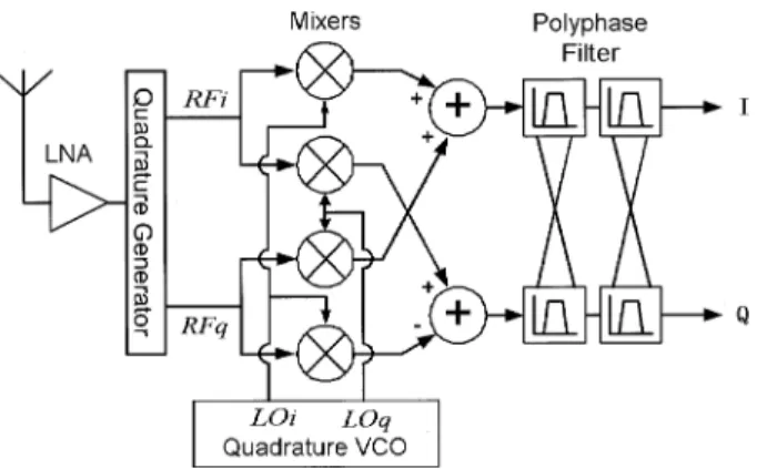
Fig. 1. Block diagram of double-quadrature receiver.
II. ARCHITECTURE ANDCIRCUITIMPLEMENTATION
A. Double-Quadrature Architecture
Fig. 1 shows the block diagram of the double-quadrature receiver. In the receiver, input signal is amplified by the LNA and then transformed to in-phase and quadrature-phase signals by quadrature generator. After mixing with quadrature local oscillator (LO) signals, the frequency is translated to intermediate frequency and the following polyphase filter will reject the image signals. As compared to low-IF architecture, the double-quadrature architecture has a better image rejection performance because the image signal crosstalk due to phase and amplitude errors of LO signals can be suppressed by separating the input RF signal into quadrature.
B. Low-Noise Amplifier and Quadrature-Generator
Fig. 2 shows the circuit diagram of the low-noise amplifier (LNA) and the quadrature generator. The low-noise ampli-fier consists of an inductively degenerated common-source differential pair whose center frequency is tuned to 5.2 GHz. The dimensions of the input transistors M1 and M2 are m m, which are optimized for minimum noise figure. The LNA provides a voltage gain of 18 dB and a noise figure of 4.36 dB.
The output signal of LNA is ac-coupled to the quadrature gen-erator. As shown in Fig. 2, a single-stage frequency-adjustable
RLC phase shifter is used to implement the quadrature
gener-ator. Ideally, the quadrature signals can be generated when (1) is satisfied:
(1)
520 IEEE JOURNAL OF SOLID-STATE CIRCUITS, VOL. 39, NO. 3, MARCH 2004
Fig. 2. Circuit diagram of the LNA and quadrature generator.
M6 and M7 are used to isolate the effect of impedance loading from the phase shifter to prevent the gain degradation of the LNA. L1 and L2 are realized by spiral inductors. The p+/n-well junction capacitors MC1 and MC2 implement the varactors and the capacitances are adjustable by adjusting the voltage . In this way, the adjustable capacitance is able to compensate the varying impedance of the inductor at different frequencies. In the frequency range of 300 MHz, the spiral model can be represented as an inductor in series with a resistor . The sum of resistances and realizes the required resistance. In this design, the simulated gain of the quadrature generator is 0 dB. The simulation also verifies that the single-stage circuit can avoid the heavy noise figure degradation because this circuit only increases 0.5 dB of noise figure. The simulated input- referred third-order intercept point (IIP3) of quadrature generator is 5 dBm.
HSPICE simulations are performed to verify the quadrature error. As shown in Fig. 3, by adjusting the control voltage from 0.9 to 1.8 V with 0.1-V increase step, the exact quadrature phase can be obtained and amplitude error varies from 0.17 dB to 0.14 dB in the frequency range 5.14–5.39 GHz. The am-plitude error increases near the edge of band because the resis-tances of R1 and R2 are fixed and the impedances of inductor and resistance become unequal as frequency varies. The simu-lation result depicts 0.17 dB of amplitude error provides image suppression of 40 dB.
Thirty Monte Carlo simulations verify the effects of com-ponent mismatch. The transistor dimensions are randomly distributed according to the sigma value provided by corner parameters specified in MOS device model, and the resistance variation is 20%. The simulation results in an image suppres-sion distribution from 65 to 40 dB at 5.25 GHz.
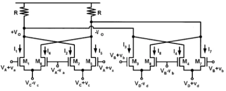
C. Mixers and Quadrature VCO and Polyphase Filter
Fig. 4 shows the circuit diagram of the four-input combiner, which is used to realize the mixing function. As ( , , , )
is substituted for ( , , , ) and ( , ,
Fig. 3. Simulated amplitude errors and IR at the outputs of the quadrature generator.
Fig. 4. Circuit diagram of four-input combiner.
, ), the downconversion function can be realized.
A circuit structure based on the even-stage ring oscillator is used to implement the integrated quadrature VCO [5]. To reduce the power consumption of four downconversion mixers, a cur-rent reuse structure is used in this design. The quadrature VCO is cascaded with four-input combiners and shares the same dc current. The simulated conversion gain is 0 dB and power con-sumption is 5.5 mW.
IEEE JOURNAL OF SOLID-STATE CIRCUITS, VOL. 39, NO. 3, MARCH 2004 521
Fig. 5. Die microphotograph of the fabricated CMOS double-quadrature receiver.
Fig. 6. Measured results concerning CP1 dB and IIP3.
A four-stage active polyphase filter [6] is connected after the mixers to filter the image signals. The filter can achieves 60 dB of image rejection over the frequency range 17–40 MHz.
III. EXPERIMENTALRESULTS
The double-quadrature receiver was designed and fabricated in 0.18- m CMOS technology. Fig. 5 shows the die microphoto-graph. The chip consumes 22.4 mW at a power supply of 1.8 V, and occupies a die area of mm .
Fig. 6 shows the result of linearity measurement. The mea-sured IIP3 is 13 dBm, and the measured input-referred 1-dB compression point (CP1dB) of the receiver is 24 dBm. The re-sult meets the requirement because CP1dB is 6 dB higher than the maximum input power level [2].
Fig. 7 shows the measured frequency response of the overall receiver. An input signal of 45 dBm is applied to keep the desired output signal and image signal in the dynamic range. The maximum gain of the desired signal is 16.5 dB and a 16-dB gain can be achieved in the frequency range from 20 to 40 MHz. The maximum gain of the image signal within the bandwidth is 34.6 dB. That is, a minimum image rejection of 50.6 dB is achieved. Table I summarizes all the measured results.
IV. CONCLUSION
A 1.8-V low-power 5-GHz CMOS front-end receiver has been proposed. The low power consumption and high image
Fig. 7. Measured frequency response of double-quadrature receiver.
TABLE I
MEASUREDPERFORMANCES OF THEDOUBLE-QUADRATURERECEIVER
rejection ability exhibit that the proposed receiver front-end is suitable for IEEE 802.11a wireless LAN applications.
REFERENCES
[1] Part 11: Wireless LAN Medium Access Control (MAC) and Physical Layer (PHY) Specifications: High Speed Physical Layer in the GHz Band, IEEE Standard 801.11a/D7.0, 1999.
[2] T. H. Lee, H. Samavati, and H. R. Rategh, “5-GHz CMOS wireless LANs,” IEEE Trans. Microwave Theory Tech., vol. 50, pp. 268–280, Jan. 2002.
[3] B. Razavi, “A 5.2-GHz CMOS receiver with 62-dB image rejection,” IEEE J. Solid-State Circuits, vol. 36, pp. 810–815, May 2001. [4] J. Crols and M. S. J. Steyaert, “A single-chip 900 MHz CMOS receiver
front-end with a high performance low-IF topology,” IEEE J. Solid-State Circuits, vol. 30, pp. 1483–1492, Dec. 1995.
[5] C.-Y. Wu and H.-S. Kao, “A 2-V low-power CMOS direct-conversion quadrature modulator with integrated quadrature voltage-controlled os-cillator and RF amplifier for GHz RF transmitter applications,” IEEE Trans. Circuits Syst. II, vol. 49, pp. 123–134, Feb. 2002.
[6] C.-Y. Chou and C.-Y. Wu, “The design of a new wideband and low-power CMOS active polyphase filter for low-IF receiver applications,” in Symp. APCCAS, Singapore, Dec. 2002, pp. 241–244.