A Design-for-Digital-Testability Circuit Structure
for
6-1 Modulators
Hao-Chiao Hong, Member, IEEE
Abstract—A design-for-digital-testability (DfDT) switched-capacitor circuit structure for testing 6-1 modulators with digital stimuli is presented to reduce the overall testing cost. In the test mode, the DfDT circuits are reconfigured as a one-bit digital-to-charge converter to accept a repetitively applied6-1 modulated bit-stream as its stimulus. The single-bit character-istic ensures that the generated stimulus is nonlinearity free. In addition, the proposed DfDT structure reuses most of the analog components in the test mode and keeps the same loads for the operational amplifiers as if they were in the normal mode. It thereby achieves many advantages including lower cost, higher fault coverage, higher measurement accuracy, and the capability of performing at-speed tests. A second-order 6-1 modulator was designed and fabricated to demonstrate the effectiveness of the DfDT structure. Our experimental results show that the digital test is able to measure a harmonic distortion lower than 106 dBFS. Meanwhile, the dynamic range measured with the digital stimulus is as high as 84.4 dB at an over-sampling ratio of 128. The proposed DfDT scheme can be easily applied to other types of6-1 modulators, making them also digitally testable.
Index Terms—Analog-to-digital converter (ADC),
design-for-testability (DFT), digitally testable, mixed-signal circuit testing,
6-1 modulator.
I. INTRODUCTION
A
DVANCED process technology nowadays enables hun-dreds of million transistors to be integrated onto a single chip, making system-on-a-chip (SoC) designs more feasible than ever. Such SoC chips usually consist of various compo-nents such as analog-to-digital converters (ADCs), digital-to-analog converters (DACs), phase-locked loops (PLLs), random logic, memory, processors, and so on. However, the ever increasing complexity and the limited observability and con-trollability of SoC chips make their testing tasks very difficult and expensive. Undoubtedly, there is a pressing need for effec-tive design-for-testability (DFT) and built-in-self-test (BIST) strategies. The scenario is to trade off the silicon area for the testing cost as the fabrication cost of each transistor keeps decreasing. In other words, reducing the testing cost and diffi-culty by adding a reasonable amount of DFT/BIST circuitry. Although such techniques have been well developed for digital circuits and memory [1], there is ample room for improvement in the analog/mixed-signal (AMS) field.Manuscript received April 4, 2006; revised March 30, 2007. This work was supported by the National Science Council, Taiwan, R.O.C., under Grant NSC93-2215-E009-050.
The author is with the Department of Electrical and Control Engineering, National Chiao Tung University, HsinChu 300, Taiwan, R.O.C. (e-mail: [email protected]).
Digital Object Identifier 10.1109/TVLSI.2007.909799
In addition, testing AMS circuits in a conventional way is in-herently exorbitant due to the expensive AMS automatic test equipment (ATE) and a long test time [2]. The long test time is mainly a result of the sequential test flow. Conventionally, the digital and AMS parts of a chip are tested sequentially even though an AMS ATE can be used to test them simultaneously. The sequential flow, nonetheless, is necessary to alleviate the in-terference between the analog signal paths and the digital ones on the device interface board (DIB). Note that any subtle in-terference and noise in the test environment can dramatically degrade the accuracy of the test results, especially for the high performance AMS circuits [2].
To tackle these challenges, using a purely digital test scheme is a promising solution. First, pure digital interfaces are insen-sitive to environmental interference and noise. Second, the dig-ital ATE employed by a digdig-ital test scheme is much cheaper. Third, the test time can be substantially reduced since the analog and digital parts now can be tested in parallel. This advantage comes from the absence of the analog signal path on the DIB. On top of all these advantages, one critical issue that needs to be addressed in order to make the digital tests viable is—can we obtain highly correlated test results to those measured by the analog tests using some lower cost digital test scheme?
A variety of AMS BIST schemes that do not require ex-ternal analog stimuli have been proposed in prior literature [3]–[13]. Among these techniques, the functional test-based BIST schemes are very appealing. In theory, they can provide the same results as the conventional analog tests. Such test schemes generate their analog stimuli on-chip by using either an embedded precision DAC [3], [7], an embedded ramp gen-erator [5], [8], [9], or an R-C exponential waveform gengen-erator [11]. These schemes are feasible either the required on-chip resource such as the precision DAC is available, or a consider-able hardware overhead is tolerconsider-able. Besides, the test accuracy relies on the performance of the embedded analog stimulus generator (ASG). For testing high resolution ADCs such as - modulators, the embedded ASG must generate a stimulus with ultra low distortion and noise which is hard to achieve.
Hafed and Roberts proposed a technique [10] that repetitively applies a pulse-density-modulated digital bit-stream to a passive R-C anti-aliasing filter (AAF) for generating the analog stim-ulus. While this method can provide high resolution stimuli, yet the passive AAF has a poor driving capability and may occupy a considerable area. Both issues are concerns for embedded applications.
The - modulation-based BIST scheme is an alternative BIST technique for sampled-data systems [14]. Fig. 1 shows its 1063-8210/$25.00 © 2007 IEEE
1342 IEEE TRANSACTIONS ON VERY LARGE SCALE INTEGRATION (VLSI) SYSTEMS, VOL. 15, NO. 12, DECEMBER 2007
Fig. 1. 6-1 modulation-based BIST scheme.
architecture. The required ASG is implemented by an embedded one-bit DAC that accepts a repetitively applied bit-stream as its stimulus. The bit-stream is synthesized by a bit-stream gener-ator (BSG) which is a single-bit, digital - modulator made of either software or hardware [15]. The single-bit character-istic ensures the DAC having no nonlinearity issue. On the other hand, the - modulator equipped with a single-bit quantizer is used as the analog response extractor (ARE) to digitize the responses of the circuit under test (CUT). Since all circuits are synchronized by the same master clock, no bulky AAF is re-quired. This BIST scheme also benefits from the robustness and simplicity of the - modulation technique. A successful im-plementation of such a BIST switched-capacitor low-pass filter was illustrated in [13].
Based on the same BIST scenario, we propose a low cost, de-sign-for-digital-testability (DfDT) circuit structure for digitally testing - modulators in this paper. As shown by our exper-imental results, the DfDT implementation achieves higher test accuracy among all previously published results to the best of our knowledge. The remainder of this paper is structured as fol-lows. Section II depicts the design and operations of the DfDT system by using a second-order - modulator example, and shows that it only induces a small circuit overhead while at-taining a high fault coverage. Following that, we discuss the method to generate the digital stimulus in Section III. The be-havioral simulation results addressing the possible limitations of using the digital stimuli are also included. The measurement
results of our experimental second-order - modulator man-ufactured in a 0.35- m mixed-signal CMOS process are shown in Section IV. They manifest the measurement accuracy and at-speed test capability of the proposed DfDT scheme. Finally, Section V draws the conclusions.
II. DESIGN-FOR-DIGITAL-TESTABILITYSECOND-ORDER - MODULATOR
A. Schematic of the Design-for-Digital-Testability Second-Order - Modulator
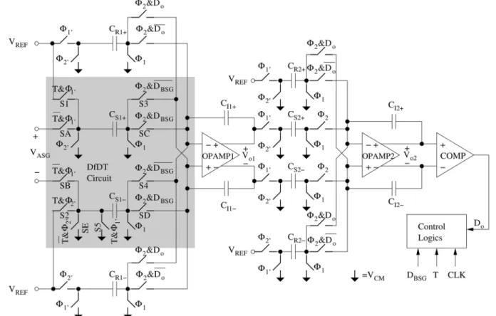
The second-order - modulator in [16] is used as an ex-ample to demonstrate the construction of a DfDT system. Fig. 2 shows the schematic of the experimental DfDT modulator under test (MUT). The proposed DfDT circuits are highlighted in the shaded area. Basically, it is composed of two cascaded summing integrators and a comparator. The comparator produces the pri-mary digital output where .
The first integrator is modified by adding five DfDT switches: – . The control commands of the associated switches ( – and – ) are also changed as those shown in Fig. 2. and are two nonoverlapped clock phases derived from the master sampling clock CLK. This DfDT - modulator is indeed a - modulation-based BIST system in which the reconfigured MUT behaves as the combination of the one-bit DAC, the CUT, and the ARE while being digitally tested.
The DfDT - modulator have two operation modes con-trolled by the test mode control pin : the normal mode and the test mode. The second integrator of the MUT keeps the same operations in both modes, while the first stage of the MUT op-erates differently.
In the normal mode, is set to 0 and the digital stimulus input is fixed to 1. The switches – of the first integrator are turned off as a result. When is active, the sampling ca-pacitors and sample the analog input . Then, the sampled charges are transferred to the integration capacitors
and during .
When operating in the test mode, the test mode control pin is set to 1. Hence, the switches SA, SB, and SE are turned off. When is active, the sampling capacitors and now sample the reference voltages and , respectively. During , the charges are transferred between
and through the switches and , or and
depending on the digital stimulus input . has a value of either 0 or 1. In this mode, the reconfigured DfDT cir-cuits can be considered as a differential 1-bit digital-to-charge converter. The single-bit characteristic ensures that the gener-ated stimulus is nonlinearity free. In addition, no bulky AAF is necessary in the test mode since all circuits are synchronized by the same master clock.
To better understand the DfDT structure, Fig. 3 shows its detailed operations in different modes and phases. Only the operations of the DfDT structure are shown since the rest of the MUT keeps the same operation in both modes. Let and be the open-loop gain and the offset voltage of the operational amplifier (OPAMP),
Fig. 2. Schematic of the proposed DfDT second-order6-1 modulator.
. Based on the charge conservation principle, the input/output (I/O) relationship of the first integrator operating in the normal mode is derived as follows:
(1) where represents the normalized test stimulus and is defined as
(2) and symbolizes the signed digital output of the MUT which is defined by
(3) Similarly, the I/O relationship of the first integrator in the test mode can be shown as
(4)
where denotes the signed digital stimulus and is de-fined as
(5) Comparing (1) with (4), it is clear that the only difference between the normal mode operation and the test mode oper-ation of the MUT is their equivalent analog stimuli. They are and , respectively. Further-more, Fig. 3 shows that the critical components, OPAMPs, drive the same capacitive loads in both modes during both phases. As a result, the design criteria of the OPAMPs in both modes are almost the same. In other words, no circuit design optimization is necessary to make a compromise in performance between the test mode and the normal mode. Such circuit optimization may be necessitated in the prior digital test schemes.
The proposed DfDT structure reuses all the OPAMPs, the ca-pacitors, the comparator, and most of the switches in the test mode, thus, it has the following advantages.
1) Low Cost: The hardware overhead of the DfDT -modulator consists of only five switches and some digital cir-cuits for generating the required control commands of the DfDT switches.
2) High Measurement Accuracy and Fault Coverage: All components are fully active in the test mode except for the switches , , and . Consequently, the DfDT structure can detect all catastrophic (open and short) faults except for the open faults of , , and . In addition, all parametric faults such as the variations of the open-loop gains, unit-gain bandwidths, and offsets of the OPAMPs, the variations of
1344 IEEE TRANSACTIONS ON VERY LARGE SCALE INTEGRATION (VLSI) SYSTEMS, VOL. 15, NO. 12, DECEMBER 2007
Fig. 3. Circuit operations of the first summing integrator in both modes. The DfDT circuits are highlighted in the shaded area. (a) During active8 in the normal mode. (b) During active8 in the normal mode. (c) During active 8 in the test mode. (c) During active 8 in the test mode.
the capacitance values, and the clock feedthrough and charge injection of most of the switches have similar impacts on the normal and the DfDT enabled outputs as illustrated by (1) and (4). As a result, the fault coverage is high and so is the measurement accuracy.
Another advantage of applying the DfDT structure is that the digital test results of some test items are more robust than the analog ones. For example, digital buffers do not induce any gain error and offset to the MUT. They also suffer less from driving capability issue. On the other hand, the analog buffers require careful design and calibration. The analog signal paths are also more susceptible to environmental interference.
3) Capability of At-Speed Tests: Since the critical com-ponents OPAMPs have the same operation conditions in the normal and the test modes as we discussed previously, the DfDT - modulator is able to operate at the rated speed in both modes.
The proposed DfDT structure can be applied to other types of - modulators easily, making them also digitally testable. B. Circuit Design
The - modulator benefits from its robustness against the impairments of the practical circuits that it consists of. To demonstrate the feasibility of the DfDT configuration in practical applications, the design of the MUT exerts the tradi-tional folded-cascode OPAMP as shown in Fig. 4. No particular design technique such as gain-boosting [17] has been applied to intentionally enhance its performance. A switched-capacitor common-mode feedback network is used to stabilize the output common-mode of the OPAMP. Table I summarizes the circuit simulation results of the OPAMP design.
The capacitive loads of the OPAMP in the first integrator are: 2 pF for the integration capacitors and , and 1 pF for the remainders. All the capacitance values of the capacitors in the second integrator are scaled down by 40% with respect to their counterparts in the first stage.
It is interesting to examine the slew rate requirements of the OPAMPs. For the switched-capacitor integrators, every evalu-ation phase can be divided into two intervals: one for the slew rate limiting operation and the other for the linear settling operation [17]. The required interval for the slew rate limiting behavior is proportional to the output step size of the integrator. Table II lists the simulated maximum step sizes of the MUT with different stimulus generators when conducting the max-imum speed tests.
The slew rate limiting interval of the first integrator is more important than that of the second one because any error or noise induced in the second integrator will be effectively attenuated by a first-order noise shaping term [16]. The maximum step size of the first integrator with the analog stimulus is about 75% of that with the digital counterpart. Since the slew rate limiting behavior occupies only a small fraction of the evaluation period, the slightly larger slew rate limiting interval of the digital stimuli only leads to a small variation of the measured rated speed.
For example, the longest slew rate limiting intervals of the first integrator in the normal and test modes are 2.3 and 3.0 ns, respectively, in the MUT design. That is, every evaluation period for the test mode operations needs an additional 0.7 ns in the worst case. It corresponds to a 4.5% rated speed reduction in the test mode. In practice, the impact may be less because only a few output steps of the first integrator are close to the maximum step size, and these transient errors can be tolerated by the -modulator itself.
Fig. 4. Simplified schematic of the folded-cascode OPAMP [13].
TABLE I
CHARACTERISTICS OF THEFOLDED-CASCODEOPAMP
TABLE II
MAXIMUMOUTPUTSTEPSIZES OF THEMUT
The design of the comparator is less critical because any noise and distortion induced by it will be attenuated by a second-order noise shaping term [16]. A conventional regenerative com-parator similar to that in [16] is used here.
III. STIMULUSGENERATION ANDBEHAVIORALSIMULATIONS Since the DfDT modulator samples the dc voltages in the test mode, there is no spectral aliasing issue. The operation of the DfDT modulator can be analyzed in the Z-domain.
A. Analysis of the MUT
The - modulator is generally characterized by its I/O re-lationship by assuming the quantization noise is white and ad-ditive [16]. Let be the normalized test stimulus. For the MUT in the normal operation, its I/O relationship can be ex-pressed by
(6)
where , and represent the
signal transfer function, the noise transfer function, and the
quantization noise of the MUT, respectively. denotes the signed digital output of the MUT whose value is either 1 or 1. On the other hand, the stimulus is first modulated by the BSG, a software single-bit - modulator, before being applied to the test mode enabled MUT. Thus, we have
(7)
where , and represent the
signal transfer function, the noise transfer function, and the quantization noise of the BSG. Here, denotes the signed digital stimulus whose value is either 1 or 1.
Since the equivalent normalized stimulus of the MUT in the test mode is , according to (6) and (7), the normalized I/O relationship of the test mode enabled MUT is derived to be
(8) Note that the test mode output of the MUT contains two shaped noise terms including
and .
Equation (8) gives an intuitive suggestion that the order of the BSG should be higher than that of the MUT so as to make
(9) within the passband. If the two shaped noises were uncorrelated, then (8) could be approximated to
(10) in the passband. The resemblance between (6) and (10) implies the measured in-band noise power might be dominated by the MUT itself as desired.
1346 IEEE TRANSACTIONS ON VERY LARGE SCALE INTEGRATION (VLSI) SYSTEMS, VOL. 15, NO. 12, DECEMBER 2007
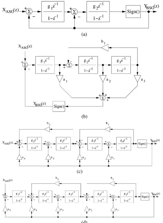
Fig. 5. Structures of the BSG candidates. (a) The multiple-feedback second-order BSG. (b) The feed-forward third-order BSG. (c) The multiple-feedback fourth-order BSG. (d) The multiple-feedback fifth-fourth-order BSG.
However, these two shaped noises do have some correlation in practice. The significance of the shaped noise correlation cannot be estimated according to the analytical results derived before. In fact, it depends on many factors such as the ampli-tude, frequency, BSG structure of the digital stimulus, as well as the circuit design of the MUT.
B. Selection of the Bit-Stream Generator
The shaped noise correlation and nonlinear nature of the MUT make the design of the digital stimulus much more com-plicated than the direct derivation from (8). For each test item, some particular BSG structure may generate the digital stimulus
achieving less shaped noise correlation than the others. To find out the most suitable one among numerous BSG candidates, behavioral simulations with a suitable behavioral mode will help. The fully-settled linear behavior plus noise (FSLB+N) model has been proposed for this application [18]. With this model, the designers can design their own BSG structures and quickly check if they are suitable for the designated tests.
1) BSG Candidates: For performance comparison, we use four BSG candidates including the multiple-feedback second-, fourth-, and fifth-order BSGs, and the feed-forward third-order BSG adopted from [19]. Fig. 5 shows the structures of these BSG candidates. Their structural coefficients are listed in Table III.
TABLE III
STRUCTURALCOEFFICIENTS OF THEBSG CANDIDATES[19]
Fig. 6. Output spectrum of the third-order BSG with the 06 dBFS test stimulus. The frequency of the stimulus tone is 21/128 K times the sampling frequency.
Fig. 6 illustrates the spectrum of the 6 dBFS digital stim-ulus generated by the third-order BSG. At an over-sampling ratio (OSR) of 128, this stimulus achieves a signal-to-noise ratio (SNR) over 92 dB, much higher than the design goal of the MUT. Therefore, it meets the requirement of (9). In fact, all BSG candidates satisfies (9) except for the second-order one. Yet they present different test results as will be discussed later. C. Behavioral Simulations
Behavior simulations with the FSLB+N model were con-ducted to select the most suitable BSG. All circuit parameters are set according to those of the practical design. The offset voltages of the OPAMP are set to 48 dBFS. All stimuli have the same frequency of 21/128K times the sampling frequency.
Fig. 7 shows the simulated SNR results at an OSR of 128. Un-like the analytical expectancy according to (10), there are 0.45 to 9.8 dB SNR differences between the analog stimuli and their digital counterparts depending on the test stimulus amplitude. It exhibits that the approximation of (10) is not so accurate even though (9) is satisfied. Indeed, the shaped noise correlation is the root cause of the SNR difference.
Note that the higher the stimulus amplitude, the larger the SNR difference. It is because the extra shaped noise power of
Fig. 7. Behavioral simulation results of the MUT’s SNRs at an OSR of 128 with the stimuli generated by various generators.
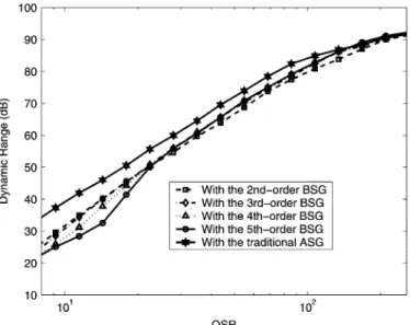
Fig. 8. Behavioral simulation results of the MUT’s DRs at different OSRs and with different stimulus sources.
the digital stimulus will overload the MUT. Simulation results shows that a test stimulus amplitude higher than 10 dBFS will overload the MUT. Once the MUT is overloaded, the basic as-sumption that its quantization noise is white and additive is get-ting worse. Therefore, the inband noise power is no longer in-dependent of the stimulus amplitude. In fact, it will increase at a rate much faster than that of the stimulus amplitude, thus leading to the droops of the digitally tested SNR curves.
Dynamic range (DR) is a common test item used to charac-terize the noise performance of a high-resolution ADC. A pop-ular definition of DR applies a 60 dBFS stimulus and then measures the SNR. The DR result is equal to the measured SNR plus 60 dB [20]. The DR of a - modulator is actually OSR dependent. That is, the MUT can trade its bandwidth off the DR. Fig. 8 shows the simulated DRs at different OSRs of the BSG candidates. The digital stimuli can provide the same DR results as the analog ones do at an OSR larger than 150. The
1348 IEEE TRANSACTIONS ON VERY LARGE SCALE INTEGRATION (VLSI) SYSTEMS, VOL. 15, NO. 12, DECEMBER 2007
Fig. 9. Micrograph of the DfDT second-order6-1 modulator.
digital stimuli generated by the second-order BSG are the only exceptions. It is due to the fact that the second-order BSG is the only candidate which fails to meet the basic requirement of (9). As a result, the in-band noise power is increased by the in-band shaped noise residue of the second-order BSG.
Although there is no significant difference among the DR re-sults of the third-, fourth-, and fifth-order BSGs at an OSR of 128, the third-order BSG is selected to test the implemented DfDT - modulator since it is the one that most closely fol-lows the curve of the traditional ASG in Fig. 8.
IV. MEASUREMENTRESULTS
The DfDT second-order - modulator has been imple-mented in a 0.35- m mixed-signal CMOS process through the service of CIC, Taiwan. Fig. 9 shows the micrograph of the MUT. The active area of the MUT is 1160 m 468 m, while the DfDT switches and the command generator occupy 2445 m . The area overhead is only 0.45%. In our layout, all of the additional DfDT circuits and routing wires were placed on the free space of the original layout, resulting in no actual area overhead.
In the following tests, the full-scale input range was set to 0.9-V. The lengths of the digital stimuli and outputs were all 128-K samples. The test stimulus is a single tone with a fre-quency of 21/128 K times the sampling frefre-quency and the pling rate is set to 32 MHz unless otherwise noticed. The sam-pling clock CLK is derived from an embedded divided-by-two circuit to guarantee an exact 50% duty cycle.
Two OSRs were used to demonstrate the effectiveness of the proposed DfDT structure for different applications. The first OSR is 128, at which the MUT has an input bandwidth up to 125 KHz. The second OSR is 512, corresponding to an input bandwidth of 31.3 KHz. The latter case is suitable for high-res-olution audio applications.
Audio Precision System II was used to generate the stimuli for the analog tests, while the digital stimuli were generated by MATLABprograms. The same logic analyzer applied the digital stimuli to the test chip and captured the primary digital output of the MUT. Our final analysis of the received digital data were done using MATLAB. The minimum-four-term window was ap-plied to all spectral analysis.
A. Amplitude Responses
Fig. 10 shows the measured SNRs at different test stimulus amplitudes in the normal mode and the corresponding results in
Fig. 10. Measured SNR versus test stimulus amplitude.
the test mode. The test stimulus amplitude sweeps from 60 to 4 dBFS.
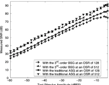
The tested DRs at an OSR of 128 with the analog and digital stimulus are 87.3 and 84.4 dB, respectively. On the other hand, the measured DRs are 93.5 and 91.2. dB at an OSR of 512. The differences between the analog and the digital tests are within 3 dB.
The SNR differences between the analog stimuli and their digital counterparts depend on the test stimulus amplitude and OSR. At an OSR of 128, they range from 1.7 to about 8.6 dB. The peak SNR of the test mode enabled MUT occurs at 6 dBFS which is 76.1 dB. A higher stimulus amplitude overloads the MUT more severely, thus degrading the tested SNR. At the same 6 dBFS test stimulus amplitude, the SNR tested with the traditional ASG is 82.0 dB, about 6 dB higher than that of the digital stimulus.
At an OSR of 512, the range of the tested SNR differences of the respective test and normal mode results narrows down to within 4 dB. Unlike the case at an OSR of 128, the maximum difference does not occur at the highest test stimulus amplitude. For the 4 dBFS tests, the SNR difference is only 2 dB. It im-plies that the major impact of overloading the MUT is on the high frequency noise power. The reason is that the second in-tegrator of the MUT suffers more from the overloaded MUT. According to the behavioral simulations, the maximal is larger than the maximal with the same stimulus. The er-rors induced by the second integrator will be attenuated by the first-order high-pass shaping term. Consequently, the low fre-quency noise performance of the MUT suffers less from over-loading. Based on the observation, we can derive an estimated SNR for a low OSR test according to the digitally measured SNR results at a high OSR. Let the ratio of the high OSR and the low OSR be . The SNR of the MUT at the low OSR can be estimated by subtracting dB from the measured SNR at the high OSR. The estimated SNR will be highly corre-lated to the corresponding analog test result if the in-band noise of the MUT in the normal operation is white.
Take the peak SNR tests of the MUT as an example, the MUT achieves an SNR of 89.4 dB at an OSR of 512 with the 4 dBFS
Fig. 11. Measured output spectra of the MUT running at 32 MHz. The test stimulus is a06 dBFS, 5.127 kHz, sinusoidal tone. (a) With the analog stimulus. (b) With the third-order digital stimulus.
digital stimulus. The MUT thereby is estimated to be able to provide an 83.4 dB peak SNR with the same 4 dBFS stimulus tone at an OSR of 128. The estimation is very close to the mea-sured result of the corresponding analog test which is 83.3 dB. The successful estimation indeed is based on the near flat noise floor of the MUT operating in the normal mode.
B. Shaped Noise Correlation and Modulator Overloading Fig. 11(a) and (b) show the measured output spectra of the MUT operating in the normal and the test mode, respectively. The cumulative total-harmonic-distortion-plus-noise (THD+N) powers with respect to the passband are also plotted. Comparing both figures side by side, the digital test generates higher noise power spectral density (PSD) around 100 KHz than the analog one. It is the result of the shaped noise correlation and modulator overloading.
In addition to the SNR, other test items can be derived from the same test as well. The measured offsets are shown by the dc terms of both spectra. They are 51.3 and 50.4 dBFS in the analog and the digital test, respectively. For measuring the offset, the digital test is more reliable since the offset measured by the analog test will be contaminated by the offsets of the analog buffers on the DIB and that of the ASG. On the other hand, the digital test result provides the pure offset of the MUT. The gain error of the MUT can be acquired from the ampli-tude difference of the stimulus tone between those in the output and the input spectra. The analog and digital tests measured the gain errors of 0.052 and 0.024 dB, respectively. Once again, the digital test gives a more precise result due to the dig-ital buffers causing no gain error.
The second- and third-harmonic distortions measured with the digital stimulus are 106 and 111 dBFS, while the analog test measured them to be 112 and 108 dBFS. In fact, the harmonic distortions in both tests are so low such that the noise power may dominate these harmonic frequency bins, in consequence, the measurement results are highly uncertain. Increasing the analysis length of the output bit-stream helps
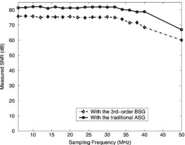
Fig. 12. Measured SNR versus sampling frequency in both modes at an OSR of 128.
lowering the noise power on the frequency bins [13]. By ana-lyzing the 256-K samples output bit-streams, the corresponding second- and third-harmonic distortions acquired with the digital stimulus and its analog counterpart are 112, 106 and 107,
108 dB, respectively. C. At-Speed Tests
Fig. 12 shows the measured SNR of the MUT versus the sam-pling frequency in both modes at an OSR of 128. The same bit-stream used in Fig. 11(b) was applied to all digital tests and the corresponding analog stimuli were applied to the analog tests. The test results show that the MUT can operate at up to 32 MHz, the rated sampling frequency, in both modes without performance degradation. Further increasing the sampling rate will degrade the tested SNR results for both modes. It justifies that the proposed DfDT structure does have the capability of performing at-speed tests.
1350 IEEE TRANSACTIONS ON VERY LARGE SCALE INTEGRATION (VLSI) SYSTEMS, VOL. 15, NO. 12, DECEMBER 2007
TABLE IV
COMPARISON OF THEANALOG ANDDIGITALTESTRESULTSWITH THESAME
06 dBFS STIMULUSTONE
Table IV summarizes the measurement results of both tests with the 6 dBFS stimulus.
V. CONCLUSION
A DfDT switched-capacitor structure based on the - mod-ulation-based BIST scheme is proposed in this paper. A physical implementation is also demonstrated by using a second-order - modulator design. In the test mode, the reconfigured MUT accepts a - modulated bit-stream as its stimulus. The pro-posed DfDT structure reuses most of the circuits in the test mode thus achieving the benefits including low cost, high fault cov-erage, and high measurement accuracy. In addition, this DfDT MUT can perform at-speed tests in the test mode as well. Our experimental results show that a harmonic distortion lower than 106 dBFS can be measured by the digital tests. Meanwhile, the measured DR with the digital stimulus is as high as 84.4 dB at an OSR of 128. Depending on test stimulus amplitude and OSR, the measured SNRs with the analog stimuli are 1.7 to 8.6 dB higher than their digital counterparts at an OSR of 128, and no more than 4 dB at an OSR of 512. The differences are the results of the extra shaped quantization noise in the digital stimuli. The proposed DfDT scheme can be applied to other types of -modulators easily to make them digitally testable as well.
ACKNOWLEDGMENT
The author would like to thank the Chip Implemen-tation Center, Taiwan, for fabricating the test chips and Dr. H.-H. S. Lee of Georgia Institute of Technology, Atlanta, for his comments on this paper.
REFERENCES
[1] L.-T. Wang, C.-W. Wu, and X. Wen, VLSI Test Principles and
Archi-tectures. San Francisco, CA: Morgan Kaufmann, 2006.
[2] M. Burns and G. W. Roberts, An Introduction to Mixed-Signal IC Test
and Measurement. Oxford, NY: Oxford Univ. Press, 2001. [3] M. F. Toner and G. W. Roberts, “A BIST scheme for a SNR, gain
tracking, and frequency response test of a Sigma-Delta ADC,” IEEE
Trans. Circuits Syst. II, Analog Digit. Signal Process., vol. 42, no. 1,
pp. 1–15, Jan. 1995.
[4] M. F. Toner and G. W. Roberts, “A frequency response, harmonic dis-tortion, and intermodulation distortion test for BIST of a Sigma-Delta ADC,” IEEE Trans. Circuits Syst. II, Analog Digit. Signal Process., vol. 43, no. 8, pp. 608–613, Aug. 1996.
[5] K. Arabi and B. Kaminska, “Efficient and accurate testing of analog-to-digital converters using oscillation-test method,” in Proc. IEEE Eur.
Des. Test Conf. (ED&TC), 1997, pp. 348–352.
[6] K. Arabi and B. Kaminska, “Testing analog and mixed-signal inte-grated circuits using oscillation-test method,” IEEE Trans.
Comput.-Aided Des. Integr. Circuits Syst., vol. 16, no. 7, pp. 745–753, Jul. 1997.
[7] K. Arabi and B. Kaminska, “On chip testing data converters using static parameters,” IEEE Trans. Very Large Scale Integr. (VLSI) Syst., vol. 6, no. 3, pp. 409–419, Sep. 1998.
[8] F. Azais, S. Bernard, Y. Bertrand, and M. Renovell, “Implementation of a linear histogram BIST for ADCs,” in Proc. IEEE Eur. Test
Work-shop (ETW), 2000, pp. 129–134.
[9] Y.-C. Wen and K.-J. Lee, “An on chip ADC test structure,” in Proc.
Des., Autom. Test Eur. (DATE), 2000, pp. 221–225.
[10] M. Hafed and G. W. Roberts, “A stand-alone integrated excitation/ex-traction system for analog BIST applications,” in Proc. IEEE Custom
Integr. Circuits Conf. (CICC), 2000, pp. 83–86.
[11] H.-K. Chen, C.-H. Wang, and C.-C. Su, “A self calibrated ADC BIST methodology,” in Proc. IEEE VLSI Test Symp. (VTS), 2002, pp. 117–122.
[12] M. Negreiros, L. Carro, and A. Susin, “Ultra low cost analog BIST using spectral analysis,” in Proc. IEEE VLSI Test Symp. (VTS), 2003, pp. 77–82.
[13] H.-C. Hong, J.-L. Huang, K.-T. Cheng, C.-W. Wu, and D.-M. Kwai, “Practical considerations in applying sigma-delta modulation-based analog BIST to sampled-data systems,” IEEE Trans. Circuits Syst. II,
Analog Digit. Signal Process., vol. 50, no. 9, pp. 553–566, Sep. 2003.
[14] J.-L. Huang and K.-T. Cheng, “A sigma-delta modulation based BIST scheme for mixed-signal circuits,” in Proc. Asia South Pacific Des.
Autom. Conf. (ASPDAC), 2000, pp. 605–610.
[15] B. Dufor and G. W. Roberts, “On-chip analog signal generation for mixed-signal built-in self-test,” IEEE J. Solid-State Circuits, vol. 34, no. 3, pp. 318–330, Mar. 1999.
[16] S. R. Norsworthy, R. Schreier, and G. C. Temes, Delta-Sigma Data
Converters: Theory, Design, and Simulation. Piscataway, NJ: IEEE Press, 1997.
[17] B. Razavi, Design of Analog CMOS Integrated Circuits. New York: McGraw-Hill, 2001.
[18] H.-C. Hong, “Improving the behavioral simulation accuracy of the de-sign-for-digital-testability second-order6-1 modulator,” in Proc. Int.
Mixed-Signals Testing Workshop (IMSTW), 2005.
[19] T.-H. Kuo, K.-D. Chen, and J.-R. Chen, “Automatic coefficients design for high-order Sigma-Delta modulators,” IEEE Trans. Circuits Syst. II,
Analog Digit. Signal Process., vol. 46, no. 1, pp. 6–15, Jan. 1999.
[20] B. Metzler, The Audio Measurement Handbook. Beaverton, OR: AUDIO PRECISION, 1993.
Hao-Chiao Hong (M’04) received the B.S., M.S.,
and Ph.D. degrees in electrical engineering from National Tsing-Hua University, HsinChu, Taiwan, in 1990, 1992, and 2003, respectively.
Since 2004, he has been with the Department of Electrical and Control Engineering, National Chiao Tung University, HsinChu, Taiwan, where he is currently an Assistant Professor. In Aug. 2001, he became the Senior Manager of the Analog IP Department, Intellectual Property Library Company, HsinChu, Taiwan. From 1997 to 2001, he was with Taiwan Semiconductor Manufacturing Company (TSMC), HsinChu, Taiwan, where he developed mixed-signal IPs for customers and process vehicles. His main research interests include the design-for-testability (DFT) and built-in self-test (BIST) techniques for mixed-signal systems and high performance mixed-signal circuit design.
Dr. Hong currently serves as Executive Secretary for Mixed-signal and RF Consortium. He is a member of the VLSI Testing Technology Forum (VTTF).


![Fig. 4. Simplified schematic of the folded-cascode OPAMP [13].](https://thumb-ap.123doks.com/thumbv2/9libinfo/7574688.125692/5.891.210.676.97.431/fig-simplified-schematic-folded-cascode-opamp.webp)