1466 IEEE TRANSACTIONS ON ELECTRON DEVICES, VOL. 56, NO. 7, JULY 2009
Optimization on MOS-Triggered SCR Structures
for On-Chip ESD Protection
Shih-Hung Chen and Ming-Dou Ker, Fellow, IEEE
Abstract—MOS-triggered silicon-controlled rectifier (SCR)
de-vices have been reported to achieve efficient on-chip electrostatic discharge (ESD) protection in deep-submicrometer CMOS tech-nology. The channel length of the embedded MOS transistor in the MOS-triggered SCR device dominates the trigger mechanism and current distribution to govern the trigger voltage, holding voltage, on resistance, second breakdown current, and ESD robustness of the MOS-triggered SCR device. The embedded MOS transistor in the MOS-triggered SCR device should be optimized to achieve the most efficient ESD protection in advanced CMOS technology. In addition, the layout style of the embedded MOS transistor can be adjusted to improve the MOS-triggered SCR device for ESD protection.
Index Terms—Electrostatic discharge (ESD), ESD protection,
silicon-controlled rectifiers (SCRs).
I. INTRODUCTION
D
UE TO THE lower breakdown voltage of the thinner gate oxide, electrostatic discharge (ESD) threat has become a major reliability concern for CMOS IC products fabricated in the advanced nanoscale CMOS processes [1], [2]. Silicon-controlled rectifiers (SCRs) have been used as on-chip ESD protection devices because of their superior area-efficient ESD robustness [1], [2]. However, SCR has some drawbacks, such as higher trigger voltage (Vt1), lower turn-on speed, and latchup concern. Therefore, the low-voltage-triggered SCR was invented to reduce the trigger voltage of SCR device [3]. Moreover, some advanced circuit techniques (the gate-coupled [4], diode-triggered [5], substrate-diode-triggered [6], and GGNMOS-diode-triggered [7] techniques) were also reported to enhance the turn-on efficiency of SCR devices for ESD protection. In addition, the lower holding voltages may suffer latchup failure (if lower than VDD operation voltage) due to external noise triggering under normal circuit operation conditions. Several previous studies had been presented to increase the holding voltage or the triggerManuscript received October 30, 2008; revised March 18, 2009. First pub-lished May 27, 2009; current version pubpub-lished June 19, 2009. This work was supported by SoC Technology Center, Industrial Technology Research Institute, Hsinchu, Taiwan. The review of this paper was arranged by Editor M. J. Kumar.
S.-H. Chen is with the Nanoelectronics and Gigascale Systems Laboratory, Institute of Electronics, National Chiao-Tung University, Hsinchu 30050, Taiwan and also with the Circuit Design Department, SoC Technology Center, Industrial Technology Research Institute, Hsinchu 31040, Taiwan.
M.-D. Ker is with the Nanoelectronics and Gigascale Systems Laboratory, Institute of Electronics, Department of Electronics Engineering, National Chiao-Tung University, Hsinchu 30050, Taiwan and also with the Department of Electronic Engineering, I-Shou University, Kaohsiung 84001, Taiwan (e-mail: [email protected]).
Color versions of one or more of the figures in this paper are available online at http://ieeexplore.ieee.org.
Digital Object Identifier 10.1109/TED.2009.2021359
current against latchup concern, such as dynamic holding volt-age SCR [8], SCR with stacked diode string [6], stacked SCR devices [9], current-triggered SCR devices [10], and high-holding low-voltage trigger SCR [11]. Recently, an initial-on ESD protection concept realized with PMOS-triggered SCR device in general CMOS processes was reported [12]. In this paper, further optimizations on the MOS-triggered SCR devices for ESD protection are studied. The modified PMOS-triggered SCR device with merged layout style is proposed to further enhance its ESD protection capability. In addition, NMOS transistors are also embedded into the SCR structures to implement NMOS-triggered SCR devices for ESD protection. These two different MOS-triggered SCR devices are compared to optimize on-chip ESD protection design in CMOS ICs.
II. SCR DEVICESWITHEMBEDDEDMOS TRANSISTORS
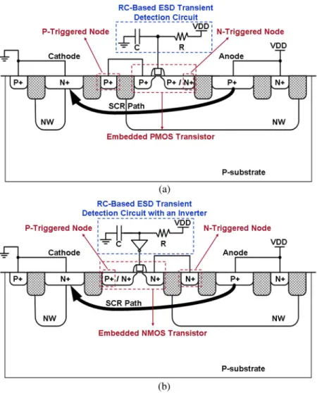
The PMOS-triggered SCR device with embedded PMOS transistor and RC-based ESD transient detection circuit is shown in Fig. 1(a) [12]. A similar SCR structure with embedded MOS transistor had been reported in the previous study [11]. The source and drain terminals of embedded PMOS transistors are, respectively, connected to the n-triggered and p-triggered nodes to synchronously generate double trigger currents into n-well and p-well of the SCR structure. The gate terminal of the embedded PMOS transistor is tied to an RC-based ESD transient detection circuit. Compared to the PMOS-triggered SCR device, the NMOS-triggered SCR device is implemented with an embedded NMOS transistor, as shown in Fig. 1(b). The source and drain terminals of the embedded NMOS transistor are, respectively, connected to the p-triggered and n-triggered nodes. The gate terminal of the embedded NMOS transistor is tied to an RC-based ESD transient detection circuit with an inverter. Due to the difference in the rise times between the ESD pulse and the VDD power-on voltage, the RC time constant in the ESD transient detection circuit is traditionally designed about 0.1–1 μs to distinguish the ESD stress condition from the normal circuit operation condition [13]. To achieve the desirable operation, the RC time constant of the ESD transient detection circuit is designed as 0.4 μs in this paper.
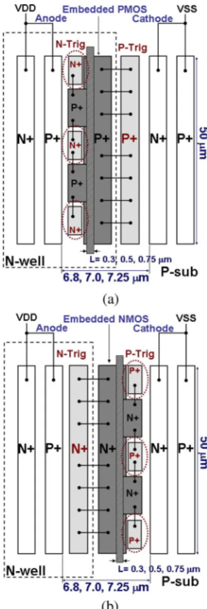
The layout top views of the MOS-triggered SCR devices are shown in Fig. 2(a) and (b). With the three different channel lengths (L) in the embedded MOS transistors, the anode-to-cathode spacings are therefore different in the MOS-triggered SCR devices. They are 6.8, 7.0, and 7.25 μm in the MOS-triggered SCR devices with channel lengths of 0.3, 0.5, and 0.75 μm in the embedded MOS transistors, respectively. The MOS-triggered SCR device with merged layout style is
KER AND CHEN: OPTIMIZATION ON MOS-TRIGGERED SCR STRUCTURES FOR ON-CHIP ESD PROTECTION 1467
Fig. 1. Cross-sectional views of (a) the PMOS-triggered SCR device with RC-based ESD transient detection circuit and (b) the NMOS-triggered SCR device with RC-based ESD transient detection circuit and an inverter.
also implemented in this paper. The p-triggered node (or the n-triggered node) was directly merged into the drain side of the embedded PMOS transistor (or the embedded NMOS transis-tor) and located across the junction between n-well and p-well. The layout top views of the MOS-triggered SCR devices with shorter anode-to-cathode spacing are shown in Fig. 3(a) and (b). This shorter anode-to-cathode spacing is only 5.1 μm when the embedded MOS transistor has a channel length of 0.3 μm. The device widths of all MOS-triggered SCR devices are kept the same at 50 μm, which have been fabricated in a 0.18-μm fully silicide CMOS process.
III. EXPERIMENTALRESULTS
A. DC Characteristics
During the normal circuit operation condition with VDD (1.8 V) and VSS (0 V) biases, the gate terminals of embedded PMOS and NMOS transistors were biased at VDD and VSS, respectively, to keep themselves off. In this paper, the dc I–V characteristics of all SCR devices are measured by Curve Tracer (Tek 370A) with the dc mode. According to the measured dc
I–V curves of the MOS-triggered SCR devices with different
channel lengths in the embedded MOS transistors (original layout style), the dc trigger voltage (Vt1) and holding voltage
(Vh) of PMOS-triggered SCR devices with 0.3-μm (0.5- and 0.75-μm) channel length are 7.30 V (7.61 and 7.83 V) and 2.82 V (3.00 and 3.12 V), respectively. On the other hand, the NMOS-triggered SCR devices with 0.3-, 0.5-, and 0.75-μm channel lengths have the Vh of 3.28, 3.63, and 3.75 V, respec-tively, with the corresponding Vt1of 6.50, 7.17, and 7.19 V. The
Vt1 and Vh are increased by increasing the channel length of the embedded MOS transistor. Moreover, the Vt1of the MOS-triggered SCR device with merged layout style is similar to that with original layout style. The merged layout style can slightly reduce the Vhof MOS-triggered SCR devices due to the shorter anode-to-cathode spacing in the layout. The dc Vt1and
Vhof PMOS-triggered and NMOS-triggered SCR devices were listed in Table I. The difference in Vt1 between the NMOS-triggered and PMOS-NMOS-triggered SCR devices can be attributed to the different drain breakdown voltages of NMOS and PMOS transistors. The influence of the embedded PMOS and NMOS transistors on Vh of SCR devices will be further discussed in the next section.
B. Turn-On Verifications
In order to observe the turn-on efficiency of MOS-triggered SCR devices with different channel lengths in the embedded
1468 IEEE TRANSACTIONS ON ELECTRON DEVICES, VOL. 56, NO. 7, JULY 2009
Fig. 2. Top views of (a) the PMOS-triggered and (b) the NMOS-triggered SCR devices with three different channel lengths of 0.3, 0.5, and 0.75 μm in the embedded MOS transistor (original layout style).
PMOS and NMOS transistors, a 5-V ESD-like voltage pulse with a fast rise time of 2 ns was applied to each VDD node (anode) of the MOS-triggered SCR device with its VSS node (cathode) grounded. The rise time of Human-Body-Model (HBM) ESD event is about 2–10 ns [14]. The voltage pulse with a rise time of 2 ns generated from a pulse generator is used to simulate the fast-rising edge of the HBM ESD event. The sharp-rising edge of the ESD-like voltage pulse will be detected by the RC-based ESD transient detection circuit to trigger on the MOS-triggered SCR devices. When the MOS-triggered SCR device is turned on, the voltage waveform on VDD node will be clamped down as the measured waveforms shown in Fig. 4(a) and (b). The PMOS-triggered SCR device (original layout style) with 0.3-μm channel length in the embedded PMOS transistor can efficiently clamp the overshooting ESD voltage pulse to a lower voltage level, as shown in Fig. 4(a). However, all of the NMOS-triggered SCR devices (original layout style) with 0.3-, 0.5-, and 0.75-μm channel lengths present better turn-on efficiency to clamp the overshooting pulse to a much lower voltage level. Due to the larger driving capability in the
Fig. 3. Top views of (a) the PMOS-triggered SCR device and (b) NMOS-triggered SCR device with merged layout style. Both anode-to-cathode spac-ings of PMOS-triggered and NMOS-triggered SCR devices are only 5.1 μm.
embedded NMOS transistor, the NMOS-triggered SCR devices exhibit better turn-on efficiency, as shown in Fig. 4(b).
C. TLPI–V Characteristics and ESD Robustness
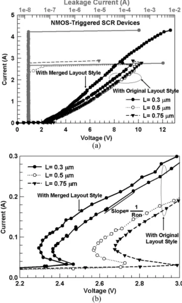
The TLP [15] I–V curves of the MOS-triggered SCR devices with different channel lengths and layout styles in the embed-ded PMOS or NMOS transistors were measured in Figs. 5(a) and (b) and 6(a) and (b), respectively. The trigger voltages (Vt1) of PMOS-triggered SCR devices are decreased from∼5.12 to
∼3.50 V when the embedded PMOS transistors are drawn with
reduced channel lengths from 0.75 to 0.3 μm, whereas those of the NMOS-triggered SCR devices are also decreased from
∼2.98 to ∼2.47 V by decreasing the channel lengths from
0.75 to 0.3 μm. The shorter channel lengths in the embed-ded MOS transistors can generate the higher trigger currents to reduce the Vt1 of the MOS-triggered SCR devices. The holding voltages (Vh) are decreased from∼3.38 to ∼2.81 V by decreasing the channel lengths from 0.75 to 0.3 μm in the embedded PMOS transistors, and those are similarly decreased
KER AND CHEN: OPTIMIZATION ON MOS-TRIGGERED SCR STRUCTURES FOR ON-CHIP ESD PROTECTION 1469
TABLE I
DEVICECHARACTERISTICS OFPMOS-TRIGGERED ANDNMOS-TRIGGEREDSCR DEVICESWITHTHREEDIFFERENTCHANNELLENGTHS INEMBEDDEDMOS TRANSISTORS ANDTWODIFFERENTLAYOUTSTYLES
Fig. 4. Under 5-V ESD-like voltage pulses with 2-ns rise time, the clamped voltage waveforms by (a) the PMOS-triggered SCR devices and (b) the NMOS-triggered SCR devices, under three different channel lengths in the embedded MOS transistors (original layout style).
from∼2.68 to ∼2.36 V by decreasing the channel lengths in the embedded NMOS transistors. The on resistances (Ron),
which are extracted from the TLP-measured I–V curves, of
Fig. 5. (a) TLP-measured I–V curves of the PMOS-triggered SCR devices with different channel lengths and different layout styles in the embedded PMOS transistors. (b) Zoomed-in view of (a) around the low-current range.
the PMOS-triggered (NMOS-triggered) SCR devices with 0.3-, 0.5-, and 0.75-μm channel lengths in the embedded PMOS transistors (NMOS transistors) are 2.71, 3.28, and 3.31 Ω (2.60, 2.81, and 2.78 Ω), respectively, as listed in Table I.
1470 IEEE TRANSACTIONS ON ELECTRON DEVICES, VOL. 56, NO. 7, JULY 2009
Fig. 6. (a) TLP-measured I–V curves of the NMOS-triggered SCR devices with different channel lengths and different layout styles in the embedded NMOS transistors. (b) Zoomed-in view of (a) around the low-current range.
In Figs. 5(a) and (b) and 6(a) and (b), each leakage current is measured under the bias of 1.8-V VDD. The second breakdown currents (It2’s) are increased from ∼3.05 to ∼3.92 A (from
∼2.67 to ∼2.78 A) by increasing the channel lengths from
0.3 to 0.75 μm in the PMOS-triggered (NMOS-triggered) SCR devices. In addition, the HBM (Machine Model, MM [16]) ESD robustness of the PMOS-triggered SCR devices with 0.3-, 0.5-, and 0.75-μm channel lengths are 5.0 kV (200 V), 6.5 kV (250 V), and 6.5 kV (300 V), respectively. They are 4.0 kV (150 V), 4.5 kV (200 V), and 4.5 kV (200 V) in NMOS-triggered SCR devices, as listed in Table I. Although the NMOS-triggered SCR devices have lower Vh and Ron, all of
the PMOS-triggered SCR devices have higher ESD robust-ness and It2. The reasons will be attributed to the different failure mechanisms in PMOS-triggered and NMOS-triggered SCR devices. Overall, the MOS-triggered SCR device with merged layout style has a lower Vh, a smaller Ron, and
a higher It2 due to a shorter anode-to-cathode spacing and higher turn-on efficiency. The It2of PMOS-triggered
(NMOS-Fig. 7. (a) Failure spot is located at the embedded PMOS transistor in the PMOS-triggered SCR device with 0.3-μm channel length. [(b) and (c)] Failure spots are located at the anode to embedded PMOS transistors in the PMOS-triggered SCR devices with 0.5- and 0.75-μm channel lengths. (d) Failure spot is located at the embedded NMOS transistor in the NMOS-triggered SCR device with 0.75-μm channel length.
triggered) SCR device with merged layout style achieves 4.17 A (4.22 A), which is over 1 A higher than that with the original layout style, as shown in Figs. 5(a) and 6(a). The HBM (MM) ESD robustness of the PMOS-triggered and NMOS-triggered SCR devices with merged layout styles are 7.0 kV (350 V) and 7.0 kV (350 V), respectively, in Table I.
IV. FAILUREANALYSIS ANDDISCUSSION
A. Failure Analysis
The failure spot investigated by SEM image is located at the embedded PMOS transistor in the PMOS-triggered SCR device with 0.3-μm channel length, as shown in Fig. 7(a). However, the failure spots are located at the anode diffusions of PMOS-triggered SCR devices with 0.5- and 0.75-μm channel lengths, as shown in Fig. 7(b) and (c). The embedded PMOS transistor with shorter channel length of 0.3 μm causes the crowding ESD currents nearby the embedded PMOS transistor and generates the huge local joule heat to destroy the embedded PMOS transistor. In addition, the embedded PMOS transistor with shorter channel length has the lower channel resistance to conduct the huge ESD current through the surface channel of the PMOS transistor to burn out itself. On the other hand, since the driving capability of the NMOS transistor is higher than that of the PMOS transistor, the failure spots on all NMOS-triggered SCR devices are located in the embedded NMOS transistors after 5-kV HBM ESD stresses, as shown in Fig. 7(d). The embedded NMOS transistors conduct huge ESD currents, and the local joule heat is produced to damage the embedded NMOS transistor from drain to source. Such a failure mechanism can explain that the ESD robustness of NMOS-triggered SCR devices was not increased by increasing the channel lengths of embedded NMOS transistors.
KER AND CHEN: OPTIMIZATION ON MOS-TRIGGERED SCR STRUCTURES FOR ON-CHIP ESD PROTECTION 1471
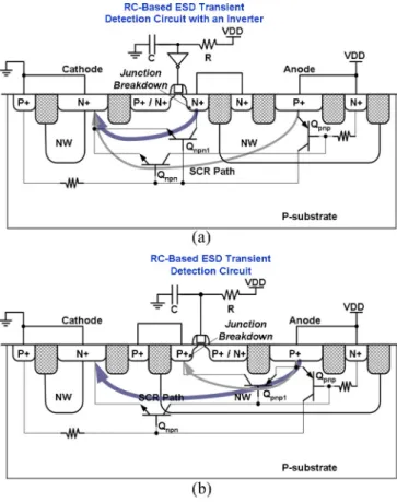
Fig. 8. Turn-on mechanisms of (a) NMOS-triggered SCR device and (b) PMOS-triggered SCR device under dc measurement with the embedded MOS transistors inOFFstate.
B. Discussion
According to the previous work [17], the holding voltage (Vh) of the SCR device under dc measurement was much lower than that of the same SCR device under TLP measurement. However, a different measured result has been observed in the NMOS-triggered SCR devices in this paper. The Vh of the NMOS-triggered SCR device under dc measurement is obvi-ously higher than that under TLP measurement. However, the
Vhof the PMOS-triggered SCR device under dc measurement is slightly lower than that under TLP measurement. The major mechanism of this abnormal phenomenon can be attributed to the different parasitic structures in these two MOS-triggered SCR devices, as shown in Fig. 8(a) and (b). When the gate terminal of the embedded NMOS transistor was biased at VSS, the drain-bulk junction breakdown of the embedded NMOS transistor in the NMOS-triggered SCR device would be induced under dc measurements with overstress voltage. The additional parasitic n-p-n bipolar transistor (Qnpn1), which is formed
by the drain-side N+ diffusion, p-substrate, and the cathode
of the NMOS-triggered SCR device, will be triggered on to conduct main currents under dc measurement, as shown in Fig. 8(a). The Vh of the NMOS-triggered SCR devices was dominated by the parasitic n-p-n bipolar transistor under dc measurement. However, such parasitic n-p-n bipolar transistor does not exist in the PMOS-triggered SCR devices. The anode of the PMOS-triggered SCR device, the n-well, and the drain-side P+ diffusion also construct another additional parasitic
p-n-p bipolar transistor (Qpnp1), as shown in Fig. 8(b). Since
the beta gain (β) of this parasitic lateral Qpnp1 is very small,
the Vhof the PMOS-triggered SCR devices is still determined by the SCR path. In addition, no junction breakdown occurs in the MOS-triggered SCR devices under TLP measurements. The embedded MOS transistors can be turned on to produce the triggering currents into n-well and p-substrate; therefore, the SCR devices will be rapidly triggered on during TLP measure-ment. The Vhof the MOS-triggered SCR devices are ruled by the SCR paths under TLP measurement.
V. CONCLUSION
The device characteristics of SCR devices with different embedded PMOS and NMOS transistors have been compared and investigated in this paper. The turn-on efficiency, such as Vt1, Vh, and Ron, of the MOS-triggered SCR devices is
enhanced by decreasing the channel lengths in the embedded MOS transistors. However, the It2 and ESD robustness of the MOS-triggered SCR devices are increased by increasing the channel lengths, particularly in the PMOS-triggered SCR devices. In addition, the embedded MOS transistor with merged layout style can obviously improve It2 and ESD robustness of the MOS-triggered SCR devices without any sacrifice of the turn-on efficiency, which will be more suitable for ESD pro-tection in nanoscale CMOS technology. Moreover, the obvious differences on the Vh of NMOS-triggered SCR devices under dc and TLP measurements have been attributed to the current distributions through the additional parasitic n-p-n bipolar tran-sistor in the SCR device structure.
REFERENCES
[1] S. Voldman, ESD: Circuits and Devices. London, U.K.: Wiley, 2006. [2] A. Amerasekera and C. Duvvury, ESD in Silicon Integrated Circuits,
2nd ed. London, U.K.: Wiley, 2002.
[3] A. Chatterjee and T. Polgreen, “A low-voltage triggering SCR for on-chip ESD protection at output and input pads,” IEEE Electron Device Lett., vol. 12, no. 1, pp. 21–22, Jan. 1991.
[4] M.-D. Ker, H.-H. Chang, and C.-Y. Wu, “A gate-coupled PTLSCR/NTLSCR ESD protection circuit for deep-submicron low-voltage CMOS ICs,” IEEE J. Solid-State Circuits, vol. 32, no. 1, pp. 38–51, Jan. 1997.
[5] J. Mergens, C. Russ, K. Verhaege, J. Armer, P. Jozwiak, R. Mohn, B. Keppens, and C. Trinh, “Diode-triggered SCR (DTSCR) for RF-ESD protection of BiCMOS SiGe HBTs and CMOS ultra-thin gate oxides,” in
IEDM Tech. Dig., 2003, pp. 21.3.1–21.3.4.
[6] M.-D. Ker and K.-C. Hsu, “Latchup-free ESD protection design with complementary substrate-triggered SCR devices,” IEEE J. Solid-State
Circuits, vol. 38, no. 8, pp. 1380–1392, Aug. 2003.
[7] C. Russ, J. Mergens, J. Armer, P. Jozwiak, G. Kolluri, and L. Avery, “GGSCR: GGNMOS triggered silicon controlled rectifiers for ESD pro-tection in deep submicron CMOS processes,” in Proc. EOS/ESD Symp., 2001, pp. 22–31.
[8] M.-D. Ker and Z.-P. Chen, “SCR device with dynamic holding voltage for on-chip ESD protection in a 0.25-μm fully salicided process,” IEEE
Trans. Electron Devices, vol. 51, no. 10, pp. 1731–1734, Oct. 2004.
[9] M.-D. Ker and K.-C. Hsu, “SCR devices with double-triggered tech-nique for on-chip ESD protection in sub-quarter-micron silicided CMOS process,” IEEE Trans. Device Mater. Rel., vol. 3, no. 3, pp. 58–68, Sep. 2003.
[10] M.-D. Ker, “Lateral SCR devices with low-voltage high-current trigger-ing characteristic for output ESD protection in submicron CMOS tech-nology,” IEEE Trans. Electron Devices, vol. 45, no. 4, pp. 849–860, Apr. 1998.
[11] J. Salcedo, J.-J. Liou, and J. Bernier, “Design and integration of novel SCR-based devices for ESD protection in CMOS/BiCMOS technologies,”
1472 IEEE TRANSACTIONS ON ELECTRON DEVICES, VOL. 56, NO. 7, JULY 2009
[12] M.-D. Ker and S.-H. Chen, “Implementation of initial-on ESD protection concept with PMOS-triggered SCR devices in deep-submicron CMOS technology,” IEEE J. Solid-State Circuits, vol. 42, no. 5, pp. 1158–1168, May 2007.
[13] M.-D. Ker, “Whole-chip ESD protection design with efficient VDD-to-VSS ESD clamp circuit for submicron CMOS VLSI,” IEEE Trans.
Electron Devices, vol. 46, no. 1, pp. 173–183, Jan. 1999.
[14] ESD Association Standard Test Method ESD STM5.1-2001, for
Electrostatic Discharge Sensitivity Testing—Human Body Model (HBM)—Component Level, 2001.
[15] T. Maloney and N. Khurana, “Transmission line pulsing techniques for circuit modeling of ESD phenomena,” in Proc. EOS/ESD Symp., 1985, pp. 49–54.
[16] ESD Association Standard Test Method ESD STM5.2-1999, for
Electro-static Discharge Sensitivity Testing—Machine Model (MM)—Component Level, 1999.
[17] A. Tazzoli, F. Marino, M. Cordoni, A. Benvenuti, P. Colombo, E. Zanoni, and G. Meneghesso, “Holding voltage investigation of advanced SCR-based protection structures for CMOS technology,”
Microelectron. Reliab., vol. 47, no. 9–11, pp. 1444–1449, Sep.–Nov. 2007.
Shih-Hung Chen received the B.S. degree from the
Department of Materials Science and Engineering, National Hu-Wei Institute of Technology, Yunlin, Taiwan, in 2000, the M.S. degree from the Institute of Materials Science and Engineering, National Chiao-Tung University, Hsinchu, Taiwan, in 2002, and the Ph.D. degree from the Institute of Electronics, Na-tional Chiao-Tung University, in 2009.
In 2002, he joined the Department of ESD and Product Engineering, SoC Technology Center, In-dustrial Technology Research Institute, Hsinchu, as an ESD Design and Product Engineer. His current research interests include the design of on-chip ESD protection circuits and product reliability of CMOS integrated circuits.
Ming-Dou Ker (S’92–M’94–SM’97–F’08) received
the Ph.D. degree from the Institute of Electronics, National Chiao-Tung University, Hsinchu, Taiwan, in 1993.
He was a Department Manager with the VLSI Design Division, Computer and Communication Re-search Laboratories, Industrial Technology ReRe-search Institute, Hsinchu. Since 2004, he has been a Full Professor with the Department of Electronics Engi-neering, National Chiao-Tung University. From 2006 to 2008, he served as the Director of Master Degree Program with the College of Electrical Engineering and Computer Science, National Chiao-Tung University, as well as the Associate Executive Director of the National Science and Technology Program on System-on-Chip in Taiwan. Since 2008, he has been the Chair Professor and Vice President of I-Shou University, Kaohsiung, Taiwan. In the field of reliability and quality design for circuits and systems in CMOS technology, he has published over 360 technical papers in international journals and conferences. He has proposed many inventions to improve the reliability and quality of integrated circuits, which have been granted with 142 U.S. patents and 144 R.O.C. (Taiwan) patents. He had been invited to teach and/or to consult the reliability and quality design for IC products by hundreds of design houses and semiconductor companies in the worldwide IC industry. His current research interests include reliability and quality design for nanoelectronics and gigascale systems, high-speed and mixed-voltage I/O interface circuits, on-glass circuits for system-on-panel applications, and biomimetic circuits and systems for intelligent prosthesis.
Prof. Ker has served as a member of the Technical Program Committee and the Session Chair of numerous international conferences. He served as the Associate Editor for the IEEE TRANSACTIONS ONVLSI SYSTEMS. He has been selected as the Distinguished Lecturer in the IEEE Circuits and Systems Society (2006–2007) and in the IEEE Electron Devices Society (2008–2009). He was the President of Foundation in Taiwan ESD Association. In 2008, he has been elevated as an IEEE Fellow with the citation of “for contributions to electrostatic protection in integrated circuits, and performance optimization of VLSI micro-systems”. In 2009, he was awarded as one of the top ten Dis-tinguished Inventors in Taiwan and also one of the top hundred DisDis-tinguished Inventors in China.
![TraditionalMLCalgorithmsmainlytacklethebatchMLCproblem,wheretheinputdataarepresentedinabatch[24,28].Nevertheless,inmanyMLCapplicationssuchase-mailcategorization[22],multi-labelexamplesarriveasastream.Onlineanalysisistherefore dimensionreducermotivatedbyma](data:image/gif;base64,R0lGODlhAQABAIAAAP///wAAACH5BAEAAAAALAAAAAABAAEAAAICRAEAOw==)