Chia-Jung Yu, and Chen-Yi Lee, Member, IEEE
Abstract—This brief presents a low-power small-area digitally
controlled oscillator (DCO). The coarse–fine architecture with binary-weighted delay stages is applied for the delay range and resolution optimization. The coarse-tuning stage of the DCO uses the interlaced hysteresis delay cell, which is power and area efficient, as compared with conventional delay cells. The glitch protection synchronous circuit makes the DCO easily con-trollable without generating glitches. A demonstrative all-digital phase-locked loop using the DCO is fabricated in a 90-nm CMOS process with an active area of 0.0086 mm2. The measured output frequency range is 180–530 MHz at the supply of 1 V. The power consumption are 466 and 357 μW at 480- and 200-MHz output, respectively.
Index Terms—All-digital phase-locked loop (ADPLL),
digi-tally controlled oscillator (DCO), interlaced hysteresis delay cell (IHDC), low power.
I. INTRODUCTION
A
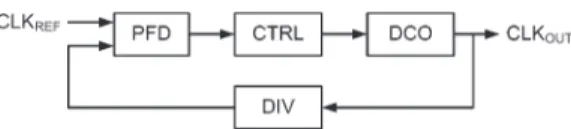
LL-DIGITAL phase-locked loops (ADPLLs) have been widely used in integrated circuits for clock generation [1]–[3]. The basic architecture of the ADPLL is composed of a digitally controlled oscillator (DCO), a frequency divider (DIV), a phase frequency detector (PFD), and a controller (CTRL), as shown in Fig. 1. Benefiting from the digital im-plementation, the functional blocks are easily manipulated with well-defined digital values. As process technology scales down, the delay timing, area, and power consumption of the func-tional blocks are substantially reduced. Therefore, the ADPLL acquires overall performance improvements in a nanometer CMOS technology [4].The DCO, which dominates the ADPLL performance, tends to generate high-frequency output with fine-resolution delay units as process technology scales down. However, in applica-tions operating at a middle-to-low or wide frequency range, the total delay time of the delay units in the DCO may not cover a large period. A straightforward approach of extending the
Manuscript received December 29, 2011; revised May 31, 2012 and July 14, 2012; accepted August 4, 2012. Date of publication September 10, 2012; date of current version October 12, 2012. This work was supported in part by the National Science Council of Taiwan under Grant NSC100-2220-E-009-016 and in part by the United Microelectronics Corporation University Shuttle Program. This brief was recommended by Associate Editor S. Levantino.
C.-Y. Yu, C.-J. Yu, and C.-Y. Lee are with the Department of Electronics Engineering and the Institute of Electronics, National Chiao Tung University, Hsinchu 300, Taiwan (e-mail: [email protected]; [email protected]).
C.-C. Chung is with the Department of Computer Science and Information Engineering, National Chung Cheng University, Chia-Yi 621, Taiwan (e-mail: [email protected]).
Color versions of one or more of the figures in this brief are available online at http://ieeexplore.ieee.org.
Digital Object Identifier 10.1109/TCSII.2012.2213357
Fig. 1. Block diagram of an ADPLL.
period is to add more delay units, which results in significant area and leakage current. An alternative approach of dividing the frequency output from the high-frequency source is area efficient but restricted in the adjustable resolution. Accordingly, the coarse–fine DCO architectures are commonly adopted to satisfy the frequency range and resolution requirements [1], [5]–[9].
With the coarse–fine DCO architecture, large coarse-tuning delay units can effectively extend the period range. The cas-caded hysteresis delay cells (CHDC) [8] are proposed for a huge delay of the single coarse-tuning unit with extremely low power consumption in a small area. Compared with conven-tional buffer [1], [6] or logic gate [5], [7], [9] approaches, the power and area are greatly reduced in the coarse-tuning stage. However, the process, voltage, and temperature (PVT) variations of the CHDC delay is high due to some weak driven internal nodes. The fine-tuning stage must cover a wider range to ensure a continuous period change and hence consumes more power and area.
In this brief, a DCO using the interlaced hysteresis delay cells (IHDCs) is proposed to achieve a large delay and low power in a small area. The IHDC interlaces the signal transitions in two series of cascaded transistors. It prevents the short-circuit current and saves the leakage current in the shared current path. All the internal nodes are rail-to-rail driven to avoid high PVT variations. Also, the glitch protection circuit using a control code resampling synchronous cells is applied for better control of the DCO. This DCO is implemented with a simple demonstrative ADPLL, which generates the output clock from 180 to 530 MHz. Consequently, the total power consumption of less than 500 μW and the 0.0086-mm2area verify its power and area efficiency. The rest of this brief is organized as follows: The architecture of the DCO and the proposed IHDCs are introduced in Section II. Section III shows the experimental results of the test chip and comparisons. Finally, Section IV concludes this brief.
II. PROPOSEDDCOANDIHDCS A. Architecture of the Proposed DCO
Fig. 2 shows the block diagram of the proposed DCO. The DCO applies the coarse–fine architecture with the 11-bit period
Fig. 2. Architecture of the proposed DCO.
control code. It is divided into four tuning stages according to the step resolution and tuning structures, namely, two coarse-and two fine-tuning stages.
The coarse-tuning stages are arranged as delay-selective paths, and each bit of the six segments, i.e., C[10]–C[5], decides which path is taken. The first coarse-tuning stage is composed of three segments. The main delay units in the segments are implemented using IHDC delay cells of different levels (IHDC-LV4, IHDC-LV3, and IHDC-LV2), which cover most of the operating period range. The IHDC can provide a larger delay with lower power consumption and smaller area occupation, as compared with conventional delay cells. The detailed cell ar-chitecture will be explained in the next discussion. The second coarse-tuning stage selects the path from zero delay to seven
ANDgates delay by the combinations of four, two, and oneAND
gates.
The fine-tuning stages are mainly composed of digitally controlled varactors (DCVs) and attached on the delay path of the coarse-tuning stages. For a fine-tuning code selection, the equivalent load on the delay path can be slightly changed and delay the clock signal transition in a picosecond resolution. The binary-weighted delay is designed for all the bits so that the period control code can be directly applied to the path selection and the DCV without a decoder. In addition, the unselected delay paths are gated by theANDgates to save power
consumption. The glitch protection circuit is designed to update the coarse-tuning code synchronously to the DCO clock signal. The clock signal passes each segment before updating the input code. Thus, the temporal instable signals in the segments are eliminated.
B. IHDC
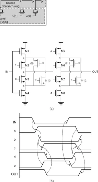
Fig. 3(a) shows the IHDC-LV2 circuit configuration. Two series of cascaded pMOS and nMOS, i.e., M1–M8, are the main delay elements. M9–M12 are for some floating-node charges/discharges. The nodes with the same name, e.g., a,
b, c, d, and e, are connected without drawing the lines. The
operating timing diagram is illustrated in Fig. 3(b). Assuming
IN is initially high and goes low, M1 is then turned on, and a
goes high. M8 is subsequently turned on, which is followed by
b going low. After that, M2 is turned on, which is followed by c going high. c turns on M7 and discharges OUT to ground.
In summary, the falling transition of the IN signal propagates through M1, M8, M2, and M7 to OUT. Similarly, the rising transition of the IN signal propagates through M4, M5, M3,
Fig. 3. (a) IHDC-LV2. (b) Timing diagram of the internal nodes of the IHDC-LV2.
and M6 to OUT. The delay path is interlaced between these two series of cascaded transistors. Although the other four transistors, i.e., M9–M12, do not contribute the delay time, those transistors connect the temporal floating nodes to a stable state. When IN goes from high to low, M4 is immediately turned off. Meanwhile, a weak low voltage will be sustained in node e. With the connection of M9, e will be subsequently charged to high. Similarly, M10, M11, and M12 keep the nodes a, b, and d to a stable state, respectively.
During the signal transition in this structure, the short-circuit path does not exist since pMOS and nMOS are turned on and off one by one in different paths. In particular, the short-circuit current dominates the power consumption in the inverter-based delay cells with the input signal of a long transition time. Therefore, the total power is largely reduced, as compared with
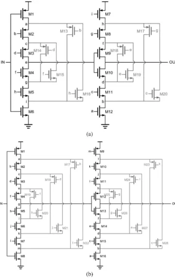
Fig. 4. (a) IHDC-LV3. (b) IHDC-LV4.
conventional delay cells. In addition, only two current paths are connected between the supply and the ground. The charge is shared by the transistors on the same path. Therefore, the leakage charge is saved by the amount that is proportional to the number of the transistors cascaded in the path. With this kind of interlaced signal pass, the transistor number in a path can be extended to enable more shared charges and a larger delay. Fig. 4(a) and (b) shows the LV3 and the IHDC-LV4, respectively.
C. Comparisons of Delay Cells
Table I lists the simulation comparisons of different delay cells in a 90-nm CMOS process. The delay cells are connected into ring oscillators whose frequency is aligned to 100 MHz by adjusting the number of delay cells. The transistor sizes and the pMOS/nMOS ratio adopted for the delay cells are the same as a balanced unit inverter. By transistor-level spice simulation, conventional delay cells like inverters (INV) [1] andAND [9] gates consume about 90- to 80-μW power. The occupied area can be viewed as the transistor counts, which are more than 800. The CHDC [8] saves 84% and 70% of the power and area, respectively, as compared with the INV gate. However,
Fig. 5. (a) Simulated DCO output period versus control code. (b) Simulated DCO power versus control code.
the PVT variations are twice of the standard logic cells due to some weak driven internal nodes. The delay variation must be covered by applying more delay cells, and the fine-tuning stage must cover a wider range. As a result, the total power and area increase instead. On the other hand, the power savings of the proposed IHDC-LV2, IHDC-LV3, and IHDC-LV4 are 12%, 29%, and 41%, respectively. All the internal nodes of the IHDC are strongly driven so that noise and delay variations due to PVT effects can be reduced. The transistor count of the IHDC-LV4 is closed to the CHDC but with better phase noise performance and smaller PVT variations of the delay. Numerous INV or AND gates can be directly replaced by the IHDC for power and area reduction.
III. IMPLEMENTATION ANDEXPERIMENTALRESULTS
The DCO is implemented in the application of the middle-to-low-frequency ADPLL. Fig. 5(a) and (b) shows the simulation results of the DCO output period versus control code and the DCO power versus control code, respectively. The first coarse-tuning stage applying the IHDC greatly expands a 3.5-ns period range with only 3 bits in the typical corner. The zoomed-in part shows good linearity in the second coarse-tuning stage and fine-tuning stages. However, the delay step of the three most significant bits is smaller, and the DCO has a discontinuity
Fig. 6. Chip photomicrograph and layout. TABLE II
MEASUREDDELAYRANGE ANDSTEPRESOLUTION OF THETUNINGSTAGES
between the codes of 2k− 1 and 2k. It can be fixed with a
larger delay step in the first coarse-tuning stage. In this ADPLL controller, some discontinuous codes of the DCO are skipped to prevent from operation failure and increasing jitter. The opera-tion of the ADPLL is explained as follows: First, the frequency acquisition is executed by binary search, which corresponds to the binary-weighted segments of the DCO. Three reference clock cycles are used for one-bit decision. The frequency lock-in time is, therefore, 33 reference clock cycles. When adjustlock-ing the fine-tuning code in the frequency acquisition, the phase acquisition is also performed. After that, phase maintaining is automatically updated according to the PFD status. The digital pulse-amplified PFD in [1] is applied in the ADPLL.
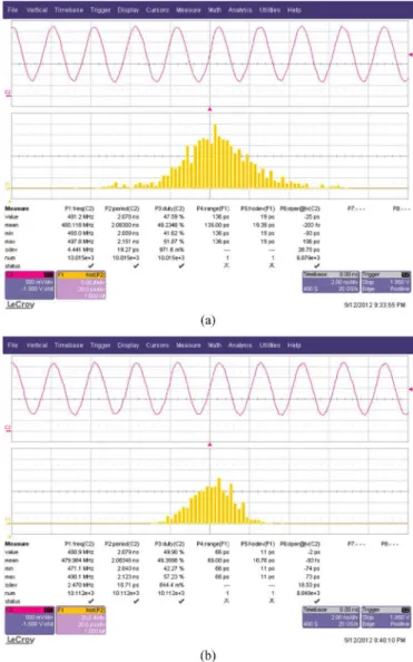
The demonstrative ADPLL is fabricated in a 90-nm CMOS technology. Fig. 6 shows the photomicrograph and the layout of the test chip. The ADPLL occupies 115 μm× 75 μm. The chip core is supplied by 1 V, and the input/output (I/O) pad is supplied by 2.5 V. The supported output frequency range is from 180 to 530 MHz. The measured delay range and the step resolution for the tuning stages are listed in Table II. The clock output is measured using the LeCroy SDA 4000A oscilloscope. The 480-MHz output waveform and period histogram gener-ated from a 12-MHz reference input are shown in Fig. 7(a). The root-mean-square (RMS) and peak-to-peak (p-p) period jitter are 19 and 136 ps, respectively. Fig. 7(b) shows the measured waveform of the free-run DCO output. The RMS and p-p period jitter are 11 and 66 ps, respectively. The jitter is mainly caused by two simplified design issues. The first design issue is the simplified controller, which updates the control code in every reference cycle and propagates the input jitter. The second is the shared I/O power ring, which couples the high-frequency signal of the output clock to the reference input clock. Those issues can be suppressed by adding a digital low-pass filter and separating the I/O power in future designs. The power consumption of the ADPLL are 466 and 357 μW at the output frequencies of 480 and 200 MHz, respectively. According to simulations, the power consumption of the DCO is 40.8% of the ADPLL at the 480-MHz output. When the lower frequency, i.e., 200 MHz, is set, the DCO power is reduced to 29.4% of the ADPLL.
Fig. 7. (a) Measured waveform and period histogram of the ADPLL output at 480 MHz. (b) Measured waveform and period histogram of the free-run DCO output at 480 MHz.
A comparison among several designs of similar frequency ranges is shown in Table III. The CHDC-based DCO [8] is the most power efficient, but only the dynamic power information is available. It is not fully ADPLL functioned. The analog PLL [13] can achieve good power efficiency by the voltage scaling and bulk-driven techniques. This work has the least power con-sumption, the finest least significant bit resolution of the DCO, and the least area occupation among the state-of-the-art PLLs. The microwatt power consumption is achieved at the nominal supply. Based on a normalized comparison, this work has the best power efficiency, which is no more than 1.785 μW/MHz. The frequency range can be easily extended by adding more IHDC stages or increasing the level of the IHDC as applications demand. The power efficiency will be also further improved.
IV. CONCLUSION
A low-power and area-efficient DCO has been presented in this brief. The proposed IHDC is applied to replace the con-ventional delay cells for power and area reduction. The binary-weighted stages with the coarse–fine architecture are designed
with the glitch protection synchronous cells. The demonstrative ADPLL is implemented in a 90-nm CMOS technology. The measurement results of the test chip show that the power consumption are 466 and 357 μW at the output frequencies of 480 and 200 MHz, respectively. This implies that our proposal looks very promising for the system-level integration with low-power features.
REFERENCES
[1] C. C. Chung and C. Y. Lee, “An all-digital phase-locked loop for high-speed clock generation,” IEEE J. Solid-State Circuits, vol. 38, no. 2, pp. 347–351, Feb. 2003.
[2] T. Olsson and P. Nilsson, “A digitally controlled PLL for SoC ap-plications,” IEEE J. Solid-State Circuits, vol. 39, no. 5, pp. 751–760, May 2004.
[3] R. B. Staszewski, J. L. Wallberg, S. Rezeq, C. M. Hung, O. E. Eliezer, S. K. Vemulapalli, C. Fernando, K. Maggio, R. Staszewski, N. Barton, M. C. Lee, P. Cruise, M. Entezari, K. Muhammad, and D. Leipold, “All-digital PLL and transmitter for mobile phones,” IEEE J. Solid-State
Circuits, vol. 40, no. 12, pp. 2469–2482, Dec. 2005.
[4] R. B. Staszewski, “State-of-the-art and future directions of high-performance all-digital frequency synthesis in nanometer CMOS,” IEEE
Trans. Circuits Syst. I, Reg. Papers, vol. 58, no. 7, pp. 1497–1510,
Jul. 2011.
[5] K. H. Choi, J. B. Shin, J. Y. Sim, and H. J. Park, “An interpolating digitally controlled oscillator for a wide-range all-digital PLL,” IEEE
Trans. Circuits Syst. I, Reg. Papers, vol. 56, no. 9, pp. 2055–2063,
Sep. 2009.
[6] H. J. Hsu and S. Y. Huang, “A low-jitter ADPLL via a suppressive digital filter and an interpolation-based locking scheme,” IEEE Trans.
Very Large Scale Integr. (VLSI) Syst., vol. 19, no. 1, pp. 165–170,
Jan. 2011.
[7] C. C. Chung and C. Y. Ko, “A fast phase tracking ADPLL for video pixel clock generation in 65 nm CMOS technology,” IEEE J. Solid-State
Circuits, vol. 46, no. 10, pp. 2300–2311, Oct. 2011.
[8] S. Y. Hsu, J. Y. Yu, and C. Y. Lee, “A sub-10 μW DCO based on HDC topologies for WBAN applications,” IEEE Trans. Circuits Syst. II, Exp.
Briefs, vol. 57, no. 12, pp. 951–955, Dec. 2010.
[9] D. Sheng, C. C. Chung, and C. Y. Lee, “An ultra-low-power and portable digitally controlled oscillator for SoC applications,” IEEE Trans. Circuits
Syst. II, Exp. Briefs, vol. 54, no. 11, pp. 954–958, Nov. 2007.
[10] M. S. W. Chen, D. Su, and S. Mehta, “A calibration-free 800 MHz fractional-N digital PLL with embedded TDC,” IEEE J. Solid-State
Cir-cuits, vol. 45, no. 12, pp. 2819–2827, Dec. 2010.
[11] W. Liu, W. Li, P. Ren, C. L. Lin, S. D. Zhang, and Y. Y. Wang, “A PVT tolerant 10 to 500 MHz all-digital phase-locked loop with coupled TDC and DCO,” IEEE J. Solid-State Circuits, vol. 45, no. 2, pp. 314–321, Feb. 2010.
[12] C. T. Wu, W. C. Shen, W. Wang, and A. Y. Wu, “A two-cycle lock-in time ADPLL design based on a frequency estimation algorithm,” IEEE Trans.
Circuits Syst. II, Exp. Briefs, vol. 57, no. 6, pp. 430–434, Jun. 2010.
[13] Y. L. Lo, W. B. Yang, T. S. Chao, and K. H. Cheng, “Designing an ultralow-voltage phase-locked loop using a bulk-driven technique,”
IEEE Trans. Circuits Syst. II, Exp. Briefs, vol. 56, no. 5, pp. 339–343,