Nano-oxidation of silicon nitride films with an atomic force microscope: Chemical
mapping, kinetics, and applications
F. S.-S. Chien, Y. C. Chou, T. T. Chen, W.-F. Hsieh, T.-S. Chao, and S. Gwo
Citation: Journal of Applied Physics 89, 2465 (2001); doi: 10.1063/1.1339212
View online: http://dx.doi.org/10.1063/1.1339212
View Table of Contents: http://scitation.aip.org/content/aip/journal/jap/89/4?ver=pdfcov
Published by the AIP Publishing
Articles you may be interested in
Chemical etching study of probe-grown ultrathin nano-oxides by atomic force microscopy
J. Appl. Phys. 99, 044301 (2006); 10.1063/1.2170592
Fabrication of nickel oxide nanostructures by atomic force microscope nano-oxidation and wet etching
J. Vac. Sci. Technol. B 21, 2599 (2003); 10.1116/1.1621655
High temperature reaction of nitric oxide with Si surfaces: Formation of Si nanopillars through nitride masking and oxygen etching
J. Vac. Sci. Technol. B 17, 1346 (1999); 10.1116/1.590758
Nanooxidation of silicon with an atomic force microscope: A pulsed voltage technique
Appl. Phys. Lett. 74, 4049 (1999); 10.1063/1.123257
Basic mechanisms of an atomic force microscope tip-induced nano-oxidation process of GaAs
J. Appl. Phys. 83, 7998 (1998); 10.1063/1.367891
Nano-oxidation of silicon nitride films with an atomic force microscope:
Chemical mapping, kinetics, and applications
F. S.-S. Chien,a)Y. C. Chou, and T. T. Chen
Department of Physics, National Tsing-Hua University, Hsinchu 300, Taiwan
W.-F. Hsieh
Institute of Electro-Optical Engineering, National Chiao-Tung University, Hsinchu 300, Taiwan
T.-S. Chao
National Nano Device Laboratory, 1001-1 Ta Hsueh Road, Hsinchu 300, Taiwan
S. Gwob)
Department of Physics, National Tsing-Hua University, Hsinchu 300, Taiwan 共Received 21 August 2000; accepted for publication 14 November 2000兲
We demonstrate that local oxidation of silicon nitride films deposited on conductive substrates with a conductive-probe atomic force microscope 共AFM兲 is a very promising approach for nanofabrication. Scanning Auger microscopy and spectroscopy are employed to verify the chemical changes after AFM-induced oxidation. Furthermore, the growth kinetics are found to have a logarithmic relationship of oxide height versus pulse duration关h⬀ln(t/t0)兴. In contrast to rather slow
thermal oxidation process, AFM-induced oxidation on silicon nitride has an anomalously high initial oxidation rate共⬃30 000 nm/s at 10 V兲 and a small onset time t0共⬃10s兲. As for the applications
in ultrahigh-density recording, an oxide dot array 共⬃100 Gbit/in.2兲 produced by this process is demonstrated. The nitride film patterned by AFM can be utilized as an etching mask to fabricate ‘‘subtractive’’ silicon nanostructures, due to the large etching selectivity of Si3N4:SiO2:Si in
various etchants. With this method, which is entirely compatible with the existing microelectronic processes, synthesis of ultrahigh packing density and ordered nanostructures could become readily achievable. © 2001 American Institute of Physics. 关DOI: 10.1063/1.1339212兴
I. INTRODUCTION
Silicon nitride 共Si3N4兲 is a dielectric material widely
used for both silicon and gallium arsenide processing due to its many superior material properties. In contrast to SiO2,
Si3N4 has unique chemical, electrical, and mechanical
prop-erties. For example, it has larger dielectric constant 共7.5 vs 3.9兲, refractive index 共2.05 vs 1.46兲, and density 共3.1 vs 2.2 g/cm3兲, as compared with SiO2.1 In one of the most
impor-tant applications, silicon nitride is used as an oxidation mask 共oxidation rate is about 100 times less than silicon兲 during the local oxidation of silicon process.2 In order to achieve high levels of integration and speed, the scaling of ultralarge-scale integrated共ULSI兲 circuits will develop into the nanom-eter regime共⬍100 nm兲 and ultrathin SiO2 gate dielectrics of
⬍2–3 nm thick will become necessary in the near future. To reduce the problem of direct tunneling in the case of ultrathin SiO2, insulators with higher dielectric constants are more
favorable as the gate dielectrics. Therefore, Si3N4and silicon oxynitride (SiOxNy兲 thin films are particularly interesting for this application.3In addition, they have been used for passi-vation layers, barrier layers against impurity diffusion, ion implant masks, gate dielectrics in dynamic random access
memory, and charge-trapping media in nonvolatile memory. The chemical selective etchings of oxide and silicon over nitride in many wet etchants4,5 or dry processes6 are also very important for the mask applications. As the decreasing of critical dimensions of ULSI circuits continues, an effec-tive and reliable patterning process for silicon nitride film on the nanometer scale becomes increasingly significant.
Many researches have demonstrated that scanning probe microscope共SPM兲 induced oxidation can be used to achieve nanometer-scale patterning on semiconductors,7–9 metals,10–12 and to fabricate various devices, e.g., metal– oxide–semiconductor field effect transistor 共MOSFET兲,13 side-gated FET,14 room-temperature single electron transistor,15 and high-aspect-ratio and high-packing-density silicon nanostructures.16 Recently, Garcı´a et al.17 reported the fabrication of high-areal-density oxide dot arrays on a hydrogen-passivated silicon substrate using noncontact atomic force microscopy共AFM兲 and Cooper et al.18reported the case of oxide array with an areal density of 1.6 Tbit/in.2 on a titanium film using a single-wall carbon nanotube grown on an AFM cantilever, revealing a new approach for ultrahigh-density data recording using AFM-induced oxida-tion. In principle, AFM-induced oxidation is a feasible pro-cess for nanometer-scale patterning on thin dielectric films deposited on conductive substrates. However, there are few reports in the literature to address this subject. In 1996, Day and Allee19reported the possibility of local oxidation on sili-con nitride using the tungsten tip of a scanning tunneling
a兲Also with: Center for Measurement Standards, Hsinchu 300, Taiwan; In-stitute of Electro-Optical Engineering, National Chiao-Tung University, Hsinchu 300, Taiwan.
b兲Author to whom correspondence should be addressed; electronic mail:
2465
0021-8979/2001/89(4)/2465/8/$18.00 © 2001 American Institute of Physics
microscope 共STM兲. Very recently, we have successfully proved the conversion of Si3N4 to SiOx with a conductive-probe AFM.20
In this article, we present the chemical analysis of the AFM-induced oxide using scanning Auger microscopy/ spectroscopy共SAM/S兲 to show that AFM-induced oxidation is an effective method for conversion of silicon nitrides to oxides. We also present the oxide growth behavior and ki-netics, although the exact AFM oxidation mechanism of sili-con nitride is still unclear at this moment. Due to the small oxide onset time, the initial growth rate of oxide on silicon nitride is two orders of magnitude higher than that on silicon. Besides, we present examples of ultrahigh-density oxide dot array and nanostructures fabricated using a Si3N4 mask to
demonstrate the prospective applications of AFM-induced oxidation on silicon nitride films.
II. EXPERIMENTAL CONDITIONS
The silicon nitride films were grown on p-type, 10⍀ cm, 共100兲-oriented Si wafers in a low pressure chemical vapor deposition 共LPCVD兲 reactor at 780 °C using a mixture of SiCl2H2 共30 sccm兲 and NH3 共130 sccm兲. Two films with
thickness of 2.5 nm 共sample A兲 and 5 nm 共sample B兲 as measured by ellipsometry were used for this study. The sample B was further densified by rapid thermal anneal at 1000 °C in a nitrogen gas for 10 s. The film thickness was reduced to 4.2 nm after annealing. Local field-induced oxi-dation was performed with a commercial AFM/STM micro-scope operated in both contact and tapping modes in ambient air. The AFM cantilevers used for oxidation were highly doped共0.01–0.025 ⍀ cm兲 n⫹-Si cantilevers. The typical tip radius, force constant, and resonance frequency of the con-tact mode cantilevers were 10 nm, 0.2 N/m, and 13 kHz, respectively. After coated with a 23 nm thick double layer of Cr and Pt/Ir, the typical tip radius became ⬃30 nm. The typical tip radius, force constant, and resonance frequency of the tapping mode cantilevers used were 10 nm, 32 N/m, and 273 kHz, respectively.
III. RESULTS AND DISCUSSIONS A. SAMÕS analysis
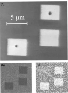
To investigate the conversion of silicon nitride to oxide, SAM/S was utilized to analyze the chemical composition. Three ⬃4⫻4 m2 squares on sample A were modified by the coated contact-mode cantilever at 0.4 m/s scan speed with a 10 V bias applied to the sample. Figure 1共a兲 is the scanning electron microscope 共SEM兲 image, which shows the layout of the squares. The SAM mappings of the nitrogen and oxygen compositions at the same AFM-oxidized region are shown in Figs. 1共b兲 and 1共c兲, respectively, in which the gray level is proportional to the amount of the specific ele-ment. Obviously, in the modified area, the nitrogen content is suppressed but the oxygen content is enhanced. Auger spec-tra taken from the as-grown and modified areas are shown in Fig. 2. Both spectra have emission peaks of Si LVV at⬃86 eV, Si KLL at⬃1620 eV, and O KLL at ⬃512 eV. However, the peak of N KLL at ⬃385 eV in the as-grown area com-pletely disappears after the film has been modified.
Mean-while, the magnitude of O KLL is much enhanced in the modified area as compared with that in the as-grown area. Therefore, it is clear that the nitrogen content is thoroughly replaced by the oxygen atoms. The results of SAM/S support the previous suggestion12 that the nitride films can be con-verted to oxides by a SPM oxidation process. The mobile oxyanions (OH⫺兲 drift toward the anodic substrate in re-sponse to the intense local field beneath the AFM tip and react with silicon nitride at the oxide/nitride interface while the nitrogen-related species drift outward.
In addition to the LPCVD films, we also applied the AFM-induced oxidation process on a single-crystal nitride film. The film was grown on a Si共111兲 substrate by thermal nitridation using ammonia. The Si共111兲-共7⫻7兲 surface was prepared in an ultrahigh vacuum 共UHV兲 chamber at a base FIG. 1. 共a兲 SEM micrograph of the AFM-induced oxide squares on the LPCVD Si3N4film. Two black spots observed on the oxide patterns result
from the electron-beam damaging during Auger analysis.共b兲 and 共c兲 SAM mappings of the nitrogen and oxygen elements on the same region. The gray scale is used to represent the element contents 共brighter regions contain more of the specified element兲.
FIG. 2. Auger electron spectra at the AFM-induced oxide and as-grown areas of the LPCVD Si3N4film.
2466 J. Appl. Phys., Vol. 89, No. 4, 15 February 2001 Chienet al.
pressure of⬍1⫻10⫺10Torr and heated to 900 °C for 20 min while NH3 gas was leaked into the chamber at a pressure of
10⫺8 Torr共⬃12 L兲. The film thickness was estimated to be 2–3 nm according to previous reports.21 The film was veri-fied in situ by a UHV STM to be a single-crystal film with an 共8⫻8兲 surface reconstruction.22
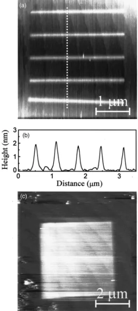
Figure 3 is the Auger spectra of the films before and after Ar ion sputtering. Before sput-tering, observations of the peak of N KLL at ⬃385 eV and the double peaks of Si LVV at⬃88 共Si–N兲 and ⬃94 共Si–Si兲 eV are the evidence for silicon nitridation. The observed double Si-LVV peaks originate from the Si–N and Si–Si bonding, respectively. The peak of C KLL at⬃267 eV indi-cates carbon contamination on the air-exposed surface. Ar-gon ion sputtering of 3 keV accelerating voltage and 300 nA ion current was employed for 5 s to eliminate contamination. The sputtering rate of the film is about⬃1–2 Å/s, therefore, corresponding to total sputtered film thickness of ⬃1 nm. The nitrogen content remains almost constant after sputter-ing, indicating the original nitride thickness was larger than 1 nm. On the other hand, the contents of oxygen and carbon were significantly reduced. The peak of elemental Si LVV at ⬃94 eV was much enhanced because the nitride film became thinner and the underlying Si substrate signal became more significant. AFM-induced oxides can also be produced on this type of film. Figures 4共a兲 and 4共b兲 are the AFM image and cross-section profile of AFM-induced oxide lines, and Fig. 4共c兲 is the AFM image of a 4⫻4 m2 oxide square produced by AFM on the film. The monolayer-height共⬃0.3 nm兲 steps in the modified square can be clearly observed even after AFM-induced oxidation, demonstrating that the AFM-induced oxidation process has an atomic smooth na-ture.
B. Oxide growth kinetics
A clear understanding of the kinetics of AFM-induced oxidation is necessary to precisely control the oxide features. In the previous studies, Teuschler et al.23 reported the em-pirical power law for the growth kinetics in which the height 共h兲 is proportional to the ␥ power of pulse duration 关h(t) ⬀t␥兴 with ␥ ⫽ 1/4 for the hydrogen-terminated Si共111兲. Based on the Cabrera–Mott theory24 of field-induced ionic transport, Stie´venard et al.25found that the oxide growth ki-netics can be described by the inverse-logarithmic form, where 1/h(t)⫽A⫺B•ln(t) 共A and B are fit parameters兲. Avouris et al.26 proposed the logarithmic kinetics in which
the oxide height is proportional to the direct logarithm of pulse duration 关h⬀ln共t兲兴 based on the data obtained by con-tact mode AFM oxidation on Si共100兲 substrates. An expo-nential dependence of oxidation rate on oxide height,
dh/dt⬀exp(⫺h/Lc兲, can be deduced from this kinetics,
where Lc is the characteristic decay length. They suggested that due to the fact that the molecular volume of SiO2 is twice as large as that of Si, the development of stress leads to an additional activation energy barrier, causing rapid de-crease of oxidation rate with increasing oxide height. Later, Calleja and Garcı´a27observed the same logarithmic behavior by noncontact mode AFM oxidation on Si共100兲.
In 1956, Uhlig28 obtained the direct-logarithmic form 关h(t)⫽k0•ln(t/⫹1)兴 of oxide growth by assuming the
oxi-dation rate is limited by the space charges increasingly trapped at and around the film–oxide interface. By using FIG. 3. Auger electron spectra taken on the single-crystal Si3N4film before
共upper spectrum兲 and after Ar ion sputtering 共lower spectrum兲.
FIG. 4. AFM images of the AFM-induced oxide on the single-crystal Si3N4
film.共a兲 Oxide lines produced with 8 V bias, 0.06m/s writing speed. The oxide height is⬃2 nm and the full width is ⬃250 nm. 共b兲 Cross-sectional height profile along the marked line in 共a兲. 共c兲 4⫻4 m2 oxide square
produced with 10 V bias and 0.32m/s writing speed. The oxide height is
⬃4.4 nm.
scanning Maxwell-stress microscopy, Dagata et al.29directly observed the trapped charge within the grown oxide. Recog-nizing that space charge buildup is the main rate-limiting step, Dagata et al.30further implemented the Uhlig model by explicitly incorporating the direct and indirect oxidation pro-cesses using the Alberty–Miller formalism31 for AFM-induced oxidation on silicon. They discovered that AFM oxi-dation on Si exhibits a two-stage kinetics. In the transient region 共⬃0.5 s for Si兲, both power law and Uhlig direct-logarithmic law are adequate in describing the oxidation be-havior. However, after entering the steady-state growth re-gion, a full consideration using the Alberty–Miller formalism is required. Recently, using the concept of space charge limited growth, Dubois and Bubendorff32 have also successfully derived the power law form of AFM-induced anodic oxidation. For this work, we are interested in the initial growth rates of AFM-induced oxide on Si3N4 .
There-fore, only the transient-region data are presented here and we use the direct-logarithmic formalism to fit our results. How-ever, a full understanding of the oxidation kinetics may re-quire data taken with longer oxidation time and a larger volt-age range.
We studied the variation of oxide height with the applied voltage and exposure time on sample B using both contact and tapping modes of AFM. The AFM-induced oxide is to-pographically protruded since the molar volume of silicon oxide is larger than that of silicon nitride. Figure 5共a兲 and 5共b兲 are plots of the oxide height 共h兲 versus applied voltage 共V兲 for 200 ms pulse duration in contact mode and 100 ms in tapping mode, respectively. A linear dependence of oxide height on bias voltage with h⬀V⫺Vthis found, where Vthis
the threshold voltage corresponding to ⬃4.3 and ⬃8 V for
contact and tapping mode, respectively. The effective elec-trical field in the tapping mode is smaller for the dynamically oscillating cantilever and higher threshold voltage is required as compared with that of the contact mode.
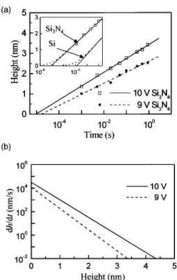
For studying the oxidation kinetics, voltage pulses of various durations 共1–1000 ms兲 were applied to the silicon nitride film and the patterned oxide dots were analyzed by contact mode AFM. Figure 6共a兲 displays the linear-log plots of oxide height versus pulse duration at biases of 9 and 10 V. The oxide height is found to increase as the logarithm of the pulse duration in both cases, that is similar to the empirical relationships obtained for silicon.26,27 Instead of the Uhlig direct-log form, h(t)⫽k0•ln(t/⫹1), where k0 andare
con-stants and h共0兲⫽0, we find that it is better to fit the data with
h(t)⫽Lc•ln(t/t0) , where Lcis a voltage-dependent constant. By extrapolating the fitted straight line as h(t)⫽Lc•ln(t/t0) to the logarithmic time axis关as shown in Fig. 6共a兲兴, we can find the oxide onset time t0, which represents the period of time required for oxide to start growth upon applying voltage pulses. Also, an exponential decay relationship of the growth rate to oxide height 关dh/dt⫽R0•exp(⫺h/Lc)兴 can be found
from the kinetic data 关Fig. 6共b兲兴, where R0⫽Lc/t0
corre-sponds to the initial oxidation rate. Although the detailed chemical reactions are rather different, the AFM-induced oxidation process on both silicon nitride and silicon obeys the same logarithmic relationship of h and t and the expo-FIG. 5.共a兲 Plot of oxide height 共h兲 vs applied bias 共V兲 using a contact mode
AFM with 200 ms pulse duration 共the set point was 1 nN and feedback servo on兲 on the LPCVD Si3N4film.共b兲 Plot of oxide height vs applied bias
using a tapping mode AFM with 100 ms pulse duration共the feedback servo off during AFM oxidation兲 on the LPCVD Si3N4film.
FIG. 6. 共a兲 Oxide height plotted as a function of pulse duration 共1 ms–1 s兲 on a logarithmic time scale at 9 and 10 V. The sample is the LPCVD grown Si3N4film. The data points represent the experimental results averaged over
several dots. In the inset, both types of logarithmic fittings关the dashed lines are fitted with h(t)⫽k0•ln(t/⫹1) and the solid lines are fitted with h(t)
⫽Lc•ln(t/t0)兴 are displayed for comparison as well as the previously re-ported result on Si共100兲 共Ref. 27兲. 共b兲 Exponential decay relation of the oxidation rate vs the grown oxide thickness关 dh/dt⫽R0•exp(⫺h/Lc)兴 de-rived from the kinetic data shown in共a兲, where R0is the initial oxidation rate and Lcis the characteristic decay length.
2468 J. Appl. Phys., Vol. 89, No. 4, 15 February 2001 Chienet al.
nential decay relationship of dh/dt and h. The logarithmic relationship appears as a universal behavior of AFM-induced oxidation for most of materials studied in the transient re-gion.
Table I shows the comparison of the oxide growth pa-rameters (Lc, t0, and R0兲 of silicon nitride and silicon
per-formed at similar sample biases. For silicon nitride, Lcis a
linear function of bias voltage, consistent with the relation-ship of oxide height and bias at a fixed oxidation time (h ⬀V⫺Vth兲. A proportional constant of characteristic decay
length to bias is determined as Lc/(V⫺Vth兲 ⫽ 0.051 nm/V. Contrary to the thermal oxidation process33where the oxida-tion rate of silicon nitride is two orders of magnitude less than that of silicon, the silicon nitride film has much higher
R0 共⬃30 000 nm/s兲 compared with that of Si共100兲 共10–250
nm/s, Refs. 26 and 27兲 under similar experimental condi-tions. Since the magnitudes of Lc of silicon nitride and
Si共100兲 at 10 V are about the same order of magnitude 共0.29–0.39 nm兲, we conclude that the high initial oxidation rate of silicon nitride might result from the small oxide onset time 共⬃10 s兲, which is two orders of magnitude smaller than that of Si共100兲 共⬃1 ms兲 关see inset of Fig. 6共a兲兴.
In our experiments, the electric field is weaker than in the case of a bare Si sample biased at the same voltage due to the starting thickness of the insulating nitride layer. The ini-tial field intensity underneath the tip apex, calculated from the formula of Konsek et al.34 for 30 nm tip radius, 10 V bias, and 4 nm separation between tip and Si substrate gap filled with Si3N4 共refractive index ⫽ 2兲 is about 1.2⫻109
V/m which is close to the critical field intensity for AFM-induced oxidation on Si共100兲.26,35,36On the other hand, the stress in silicon nitride films grown on silicon substrates is known to be tensile (⬃1⫻109 dyn/cm2兲, while the stress in silicon oxide films grown on silicon substrates is compres-sive (⬃3⫻109 dyn/cm2兲.6Therefore, the mismatch between
SiOxand Si3N4 is larger than that between SiOxand Si. As a result, the AFM-induced oxide grown on silicon nitride con-tains more stress than that in the AFM-induced oxide grown on silicon substrates. Because of weaker electric field and larger compressive stress in the AFM-induced SiOx, both
thickness-limited24 and stress-limited26 kinetic models can-not account for the anomalously high oxidation rate observed on Si3N4. In addition, compared with the rate coefficient A
⬵1 nm/min2/3 (h⫽At2/3兲 for the wet thermal oxidation at
1100 °C and under 0.95 atm of water vapor,37and the rate of
0.82 nm/min for traditional anodic oxidation38 with a field intensity of 1.9⫻109V/m at 7.5 mA/cm2, AFM-induced oxi-dation rate of Si3N4is many orders of magnitude faster than
the conventional methods.
C. Image reversal
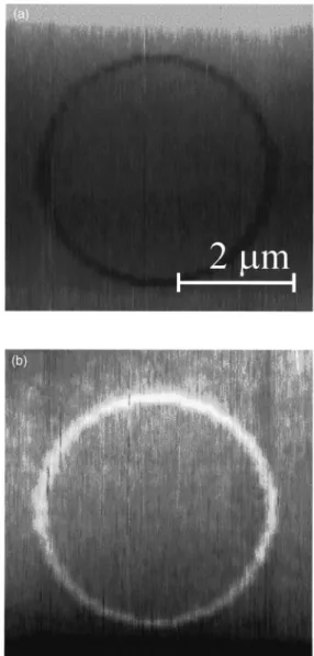
During our experiments, we sometimes observed the contrast reversal of contact-mode images of AFM-induced oxide taken interleavely with opposite-direction scans either bottom to top followed by top to bottom or left to right followed by right to left after the silicon cantilevers 共metal coated or uncoated兲 had been used extensively. In Figs. 7共a兲 and 7共b兲, a 4.5m diameter oxide circle was produced by 10 V pulses and imaged with interleaved scans. A protruded topography of 1.5 nm height was recorded from the bottom-to-top scan, while a depressed one of 1.0 nm depth was ob-tained from the top-to-bottom scan. Occasionally, the ‘‘ap-parent’’ height or depth can be as large as 100 nm. Definitely, the real AFM-induced oxide height cannot be so FIG. 7. 共a兲 and 共b兲 Contrast-reversed AFM images of an AFM-induced oxide circle on the LPCVD Si3N4 film taken with interleaved dual-scan
mode共bottom-to-top and top-to-bottom scanning direction, respectively兲. TABLE I. Growth kinetic parameters of AFM-induced oxidation on silicon
nitride and silicon.
Bias共V兲 Lc共nm兲 t0a共s兲 R0b共nm/s兲 Si3N4Contact mode 10 0.29 8.7⫻10⫺6 3.3⫻10 4 9 0.24 1.9⫻10⫺5 1.3⫻104 Sic共Ref. 26兲 10 0.39 4⫻10⫺2 9.8 Sid共Ref. 27兲 10 0.35 1.3⫻10⫺3 250
aDetermined by the intercept at the logarithmic t axis of the fitted line. bDerived from L
c/t0. cBy contact mode AFM, L
cis 0.9 nm⫻log10(e). d
By noncontact mode AFM, Lcis 0.1⫹0.03⫻10–0.0005⫻10
2共nm兲 and t 0 ⫽exp(⫺b/Lc), where b⫽⫺2.1⫹0.5⫻10– 0.006⫻10
2共nm兲.
large. Such a topographic reversal phenomenon was also ob-served for the AFM-induced oxide on silicon substrates. We believe that the space charges trapped in the grown oxide cause the image reversal. Space charges exert additional forces on the worn cantilevers and cause the response of the optical-lever feedback system39to maintain a constant bend-ing of the cantilever. Throughout our oxidation experiments discussed above for kinetics study, we always took AFM images in both scan directions to make sure that nearly iden-tical oxide topographic heights were obtained, excluding fac-titious effects from the trapped space charges.
IV. APPLICATIONS FOR DATA RECORDING AND NANOSTRUCTURE FABRICATION
Two of the most prospective applications of AFM-induced oxidation are ultrahigh-density data recording and AFM nanolithography process. In this section, we will present examples of AFM-induced oxidation on silicon ni-tride films for high-density surface modification and nano-structure fabrication. Shown in Fig. 8, we generated an oxide dot array with an areal density of ⬃100 Gbit/in.2 on sample B by applying pulses of ⫹9 V and 5 ms duration on the predetermined locations with a tip moving speed of 0.5
m/s. The total writing time is ⬃30 s for this array. The oxide formation is very reproducible and uniform with⬃45 nm dot diameter and ⬃1.2 nm oxide height. The AFM-induced oxidation on nitride film can be used as a write-once and read-many data recording technique with a higher areal density than the predicted superparamagnetic limit for the magnetic recording. Compared with hydrogen-passivated silicon substrates and titanium films oxidized in ambient, silicon nitride film is more superior as a data recording me-dium due to its resistance to oxidation under ambient condi-tions. Additionally, the high initial oxidation rate of silicon
nitride requires a shorter writing time, so higher recording speed can be achieved. It should be noted that the slow probe speed共0.5m/s兲 used here is only due to the instrumentation limit. With the current advances in high-speed,40 large-area,41 and parallel-probe42,43methods, the fundamen-tal limit to the writing speed using this approach is the initial oxidation rate.
The patterned nitride films can be used as etch masks due to the large etch selectivity of silicon nitride to oxide and silicon. The etching rates in 1% HF solution determined by ellipsometry are 0.01 nm/s for the sample B and 0.27 nm/s for AFM-induced oxide, corresponding to an etch selectivity of 27. Therefore, HF dipping can remove the AFM-induced oxide without substantial etching to the nitride film. The pat-terned windows, exposing the Si substrate, can be used for subsequent fabrication process development of nanostruc-tures.
The etching rate of silicon nitride film in a KOH solution is very slow. Under some conditions,4 the selectivity of Si/ Si3N4in a KOH solution is extremely high共1000:1兲. For the
usage of the AFM oxidation technique, a thin mask film is preferred to produce high-areal-density patterned Si-exposing windows. Hence, before patterning, the nitride film 共sample B兲 was thinned to 3 nm thick 共measured by ellip-sometry兲 by dipping in a 1% HF solution for 120 s. Figure 9 shows the process to produce a V-groove Si structure. First, oxide lines parallel to the 具110典 direction were written with 10 V bias and 0.08m/s writing speed关Fig. 9共a兲兴. The oxide is 2 nm high and with a full width at half maximum 共FWHM兲 of 210 nm. After the sample was dipped in a 1% HF solution for 20 s at 26 °C, the oxide lines were selec-tively removed and the topography converted to 3 nm deep trenches with a FWHM of 230 nm关Fig. 9共b兲兴. The conver-sion ratio of total oxide volume to the consumed silicon vol-ume defined by total oxide height divided by the buried ox-ide depth is about 1.67. After subsequent etching in a 20 FIG. 8. Oxide dot array of 100 Gbits/in.2bit areal density on the LPCVD
Si3N4film. This dot array is obtained by applying pulses of⫹9 V and 5 ms
duration on the predetermined locations with a tip moving speed of 0.5
m/s. The total writing time is⬃30 s for this array.
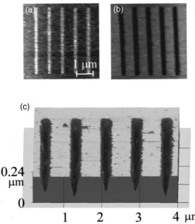
FIG. 9. 共a兲 AFM image of oxide lines on the LPCVD Si3N4 film. 共b兲
Trenches on the same region after dipping in HF solution.共c兲 AFM image of the V-grooved Si structure on the same region after KOH etching.
2470 J. Appl. Phys., Vol. 89, No. 4, 15 February 2001 Chienet al.
wt % KOH solution for 20 s at 50 °C to transfer the pattern into silicon substrate, the V-groove terminal geometry is formed by two intersecting 兵111其 crystal planes because of the anisotropic etching of silicon in KOH 关Fig. 9共c兲兴. The
V-groove opening on the surface is about 350 nm and depth
is 150 nm.
Figures 10共a兲 shows an example of inverted pyramid pit array in Si. First, an oxide dot array pattern was made by applying⫹9 V pulses of 5 ms duration. The produced oxide dots have an average diameter of ⬃60 nm and a protruded oxide height of⬃2 nm. After pattern transfer using aqueous KOH, each oxide dot converts to a⬃60⫻60 nm2 pit关Fig. 10共b兲兴. The inverted pyramidal etching pits, independent of the mask opening shape, are formed with four intersecting 兵111其-crystal-planes. And the etched depth is self-limited by the terminal etch geometry. This ‘‘subtractive’’ process could be used for fabricating nanostructures from thin films or multilayered structures, or as high-density read-only memory. Additionally, the ‘‘subtractive’’ structures can be utilized as templates for selective growth since the deposited materials tend to grow over the unmasked silicon surfaces. Recently, single-crystal silicon dots and lines have been suc-cessfully grown by selective CVD with AFM-patterned Si3N4/SiO2bilayer growth masks.44
V. CONCLUSIONS
SAM and SAS have been used to prove the conversion of LPCVD-grown Si3N4 to SiOx by a conductive-probe
AFM. The electrical field under the AFM tip promotes the bi-directional diffusions of O- and N-related species, al-though the exact reaction paths are still unknown. We also show that the AFM-induced oxidation performed on the
single-crystal silicon nitride film is an atomic smooth pro-cess. In the study of oxidation kinetics, the oxide height is found to be linearly proportional to the bias applied to the sample in both contact and tapping modes of AFM. In addi-tion, the oxide growth kinetics obeys the logarithmic rela-tionship of oxide height and pulse duration as h(t)⫽Lc •ln(t/t0) , which is similar to the previous results on Si共100兲
conducted by contact and noncontact modes. We find that the initial oxidation rate R0can be related to Lc/t0. Due to its
anomalously small oxide onset time t0 共⬃10 s兲, the initial
growth rate共⬃30 000 nm/s at 10 V兲 of oxide on nitride films is two orders of magnitude higher than that on silicon sub-strates under similar conditions. It is surprising that AFM-induced oxidation on elementary materials 共e.g., Si兲 and on compounds 共e.g., Si3N4兲 has the same growth kinetics and
Si3N4, traditionally used as an oxidation mask, has an
ex-tremely high initial oxidation rate. The role of nitrogen seems to be critical for this process. Further studies are nec-essary to reveal the exact cause of these phenomena.
For practical applications, we have demonstrated two ex-amples to show the feasible applications of AFM oxidation of nitride films on the nanometer scale. First, the AFM oxi-dation of nitride films can be employed for ultrahigh-density 共⬃100 Gbit/in.2兲 data recording with the advantages of high
writing speed and resistance to oxidation under ambient con-ditions. Second, with the large etching selectivity of silicon and oxide to nitride, the patterned nitride film can be em-ployed as an etching mask to fabricate subtractive nanostruc-tures共e.g., V-grooves and inverted pyramid pit array兲, which can be used as templates for selective-area growth共an ‘‘ad-ditive’’ process兲 or nanomechanical devices.
ACKNOWLEDGMENTS
The authors thank Dr. J. A. Dagata 共NIST兲 for useful discussions on the AFM oxidation kinetics, J.-W. Chang and S.-W. Lin for technical assistance. This work was partly sup-ported by the National Science Council共Contract Nos. NSC-89-2112-M-007-077 and NSC-89-2112-M-009-071兲 and the Program for Promoting Academic Excellence of Universities 共Contract Nos. 89-FA04-AA and 89-E-FA06-I-4兲, the Min-istry of Education, Taiwan.
1S. M. Sze, Physics of Semiconductor Devices, 2nd ed.共Wiley, New York,
1981兲, p. 852.
2S. A. Campbell, The Science and Engineering of Microelectronic
Fabri-cation共Oxford University Press, New York, 1996兲, Chap. 15, p. 390.
3
Fundamental Aspects of Ultrathin Dielectrics on Si-Based Devices, edited by E. Garfunkel, E. P. Gusev, and A Vul’共Kluwer, Dordrecht, 1998兲.
4Etch rate selectivity of Si
3N4:SiO2:Si in diluted HF共40%兲 at room
tem-perature is about 1:⬎100:0.1 and in aqueous KOH 共30 wt %兲 at 60 °C 1:⬎14:⬎ 2600; S. D. Collin, in Semiconductor Micromachining, edited by S. A. Campbell and H. J. Lewerenz 共John Wiley & Sons, Chichester, 1998兲, Vol. 2, Chap. 2, p. 57 and p. 65.
5Etch rate selectivity of Si
3N4:SiO2:Si in H3PO4 共94.5%兲 at 180 °C is
about 10:⬍1:0.3; W. van Gelder and V. E. Hauser J. Electrochem. Soc.
114, 869共1967兲.
6M. Madou, Fundamentals of Microfabrication共CRC, Boca Raton, 1997兲,
Chaps. 2 and 5.
7J. A. Dagata, J. Schneir, H. H. Harary, C. J. Evans, M. T. Postek, and J.
Bennett, Appl. Phys. Lett. 56, 2001共1990兲.
8J. A. Dagata, W. Tseng, J. Bennett, C. J. Evans, J. Schneir, and H. H.
Harary, Appl. Phys. Lett. 57, 2437共1990兲. FIG. 10. 共a兲 AFM image of an array of inverted pyramid pits on the Si
substrate.共b兲 Perspective view of a single inverted pyramid pit.
9E. S. Snow and P. M. Campbell, Appl. Phys. Lett. 64, 1932共1994兲. 10
H. Sugimura, T. Uchida, N. Kitamura, and H. Masuhara, Jpn. J. Appl. Phys., 32, L553共1993兲.
11D. Wang, L. Tsau, K. L. Wang, and P. Chow, Appl. Phys. Lett. 67, 1295 共1995兲.
12
S. Gwo, C.-L. Yeh, P.-F. Chen, Y.-C. Chou, T. T. Chen, T.-S. Chao, S.-F. Hu, and T.-Y. Huang, Appl. Phys. Lett. 74, 1090共1999兲.
13S. C. Minne, H. T. Soh, Ph. Flueckiger, and C. F. Quate, Appl. Phys. Lett. 66, 703共1995兲.
14P. M. Campbell, E. S. Snow, and P. J. McMarr, Appl. Phys. Lett. 66, 1388 共1995兲.
15K. Matsumoto, M. Ishii, K. Segawa, Y. Oka, B. J. Vartanian, and J. S.
Harris, Appl. Phys. Lett. 68, 34共1996兲.
16F. S.-S. Chien, C.-L. Wu, Y.-C. Chou, T. T. Chen, S. Gwo, and W.-F.
Hsieh, Appl. Phys. Lett. 75, 2429共1999兲.
17
R. Garcı´a, M. Calleja, and H. Rohrer, J. Appl. Phys. 86, 1898共1999兲.
18E. B. Cooper, S. R. Manalis, H. Fang, H. Dai, K. Matsumoto, S. C. Minne,
T. Hunt, and C. F. Quate, Appl. Phys. Lett. 75, 3566共1999兲.
19H. C. Day and D. R. Allee, Nanotechnology 7, 106共1996兲. 20
F. S.-S. Chien, J.-W. Chang, S.-W. Lin, Y.-C. Chou, T. T. Chen, S. Gwo, T.-S. Chao, and W.-F. Hsieh, Appl. Phys. Lett. 76, 360共2000兲.
21I. J. R. Baumvol, Surf. Sci. Rep. 36, 1-166共1999兲.
22S. Gwo, C.-L. Wu, F. S.-S. Chien, and T. Yasuda, Jpn. J. Appl. Phys. 共submitted兲.
23
T. Teuschler, K. Mahr, S. Miyazaki, M. Hundhausen, and L. Ley, Appl. Phys. Lett. 67, 3144共1995兲.
24N. Cabrera and N. F. Mott, Rep. Prog. Phys. 12, 163共1948–1949兲. 25D. Stie´venard, P. A. Fontaine, and E. Dubois, Appl. Phys. Lett. 70, 3272
共1997兲. 26
Ph. Avouris, T. Hertel, and R. Martel, Appl. Phys. Lett. 71, 285共1997兲.
27M. Calleja and R. Garcı´a, Appl. Phys. Lett. 76, 3427共2000兲. 28H. H. Uhlig, Acta Metall. 4, 541共1956兲.
29J. A. Dagata, T. Inoue, J. Itoh, and H. Yokoyama, Appl. Phys. Lett. 73,
271 共1998兲; J. A. Dagata, T. Inoue, J. Itoh, K. Matsumoto, and H. Yokoyama, J. Appl. Phys. 84, 6891共1998兲.
30J. A. Dagata, F. Perez-Murano, G. Abadal, K. Morimoto, T. Inoue, J. Itoh,
and H. Yokoyama, Appl. Phys. Lett. 76, 2710共2000兲.
31
R. A. Alberty and W. G. Miller, J. Chem. Phys. 26, 1231共1957兲.
32
E. Dubois and J.-L. Bubendorff, J. Appl. Phys. 87, 8148共2000兲.
33A. E. T. Kuiper, M. F. C. Willemsen, J. M. L. Mulder, J. B. Oude
Elf-erink, R. Erens, F. H. P. M. Habraken, and W. F. van der Weg, J. Vac. Sci Technol. B 7, 455共1989兲.
34S. L. Konsek, R. J. N. Coope, T. P. Pearsall, and T. Tiedje, Appl. Phys.
Lett. 70, 1846共1997兲.
35F. Marchi, V. Bouchiat, H. Dallaporta, V. Safarov, D. Tonneau, and P.
Doppelt, J. Vac. Sci. Technol. B 16, 2952共1998兲.
36
P. A. Fontaine, E. Dubois, and D. Stie´venard, J. Appl. Phys. 84, 1776
共1998兲.
37T. Enomoto, R. Ando, H. Morita, and H. Nakayama, Jpn. J. Appl. Phys. 17, 1049共1978兲.
38T. B. Tripp, J. Electrochem. Soc. 117, 157共1970兲.
39D. Sarid, Scanning Force Microscopy, 2nd ed.共Oxford University Press,
New York, 1994兲, Chap. 10.
40S. C. Minne, G. Yaralioglu, S. R. Manalis, J. D. Adams, J. Zesch, A.
Atalar, and C. F. Quate, Appl. Phys. Lett. 72, 2340共1998兲; S. C. Minne, S. R. Manalis, and C. F. Quate, Bringing Scanning Probe Microscopy Up To Speed共Kluwer, Boston, 1999兲.
41S. C. Minne, J. D. Adams, G. Yaralioglu, S. R. Manalis, A. Atalar, and C.
F. Quate, Appl. Phys. Lett. 73, 1742共1998兲.
42P. Vettiger, J. Brugger, M. Despont, U. Drechsler, U. Du¨rig, W. Ha¨berle,
M. Lutwyche, H. Rothuizen, R. Stutz, R. Widmer, and G. Binnig, Micro-electron. Eng. 46, 11共1999兲.
43G. Binnig, M. Despont, U. Drechsler, W. Ha¨berle, M. Lutwyche, P.
Vet-tiger, H. J. Mamin, B. W. Chui, and T. W. Kenny, Appl. Phys. Lett. 74, 1329共1999兲.
44
T. Yasuda, S. Yamasaki, and S. Gwo, Appl. Phys. Lett. 77, 3917共2000兲; S. Gwo, T. Yasuda, and S. Yamasaki, J. Vac. Sci. Technol. A 共to be published兲.
2472 J. Appl. Phys., Vol. 89, No. 4, 15 February 2001 Chienet al.