國
立
交
通
大
學
電子工程學系 電子研究所碩士班
碩
士
論
文
全數位寬電壓範圍寬頻率範圍延遲鎖定迴路時脈產生
器設計
An All-Digital Wide Power Supply Range And Wide
Frequency Range DLL-Based clock Generator
研 究 生:張益銘
指導教授:黃 威 教授
全數位寬電壓範圍寬頻率範圍延遲鎖定迴路時脈產生
器設計
An All-Digital Wide Power Supply Range And Wide
Frequency Range DLL-Based clock Generator
研 究 生:張益銘 Student:Yi-Ming Chang
指導教授:黃 威 教授 Advisor:Prof. Wei Hwang
國 立 交 通 大 學
電 子 工 程 學 系 電 子 研 究 所
碩 士 論 文
A Thesis
Submitted to Department of Electronics Engineering & Institute of Electronics College of Electrical Engineering and Computer Engineering
National Chiao Tung University in partial Fulfillment of the Requirements
for the Degree of Master
in
Electronics Engineering July 2009
Hsinchu, Taiwan, Republic of China
全數位寬電壓範圍寬頻率範圍延遲鎖定迴路時脈產生
器設計
學生:張益銘 指導教授:黃 威 教授
國立交通大學電子工程學系電子研究所
摘 要
本論文提出一個全數位式、寬電壓範圍、寬頻率範圍延遲鎖定迴路時脈產生 器。藉由高穩健性的電路技巧使用,本電路能正常操作在寬電壓範圍。此外,為 了達到快速鎖定,以及增加操作頻率範圍並且同時避免多諧鎖定,提出了一個可 變性連續近似暫存器搜尋演算法,其特點在於結合頻率估計選擇器,提供不同的 初始延遲時間已達到上述的功能。一個連續近似暫存控制器應用在多相位延遲鎖 定迴路於UMC 90nm CMOS 技術,模擬結果顯示,在 1.0V 工作電壓下,可操作 頻率為250MHz 到 1.25GHz ;在 0.3V 工作電壓下操作頻率為 13MHz 到 75MHz。 一個125MHz 到 2.5GHz 全數位延遲鎖定迴路時脈產生器實現在 UMC 90nm CMOS 技術。為了達到動態調整頻率或電壓來減少功率消耗,一個穩健且可程式 化的頻率倍乘器被提出。此外,一個新型的漏電流減少數位控制延遲元件被提 出,根據模擬顯示,可減少 10%漏電流且不減緩電路的操作頻率。本時脈產生器 其最大消耗的總功率為 0.71 毫瓦當操作在 500MHz 且產生 250MHz 、500MHz 、 1GHz 及 2GHz 等四種不同頻率。本論文提出的延遲鎖定迴路可穩定地使用在各 種嵌入式記憶體應用及可攜式產品中。An All-Digital Wide Power Supply Range And Wide
Frequency Range DLL-Based clock Generator
Student: Yi-Ming Chang Advisors: Prof. Wei Hwang
Department of Electronics Engineering & Institute of Electronics
National Chiao-Tung University
ABSTRACT
An all-digital wide power supply range wide frequency range DLL-based clock generator is proposed in this thesis. In order to operate in wide power supply range, the robust circuit methodology is used in this design. Besides, an adaptive successive approximation register-controlled (ASAR) search algorithm is proposed to extend the locking range and avoid harmonic lock at the same time. An ASAR based controlled is adopted in multiphase DLL implemented in UMC 90nm CMOS technology. The simulation results show that, the operating frequency is from 250MHz to 1.25GHz at 1.0V, and 13MHz to 75MHz at 0.3V, respectively.
A 125MHz-2.5GHz all-digital DLL-based clock generator has been designed in UMC 90nm CMOS technology. In order to achieve dynamic frequency/voltage scaling application, the robust and programmable frequency multiplier is proposed. Besides, the novel leakage-reduced delay unit is proposed to take advantages of mitigating 10% leakage current, insensitive to PVT variations, and not degrading operating frequency of circuit. The simulation results show the proposed DLL-based clock generator exhibits maximum power dissipation 0.71mW when operate in 500MHz, generating 250MHz, 500MHz, 1GHz, and 2GHz four different frequency at the same time. The presented DLL clock generator can be robustly used in embedded memory applications and portable device.
CONTENT
摘 要………...………..I ABSTRACT………..…………II CONTENT……….………..III LIST OF TABLES………..……..……....VI LIST OF FIGURE………..…………VIICHAPTER 1 INTRODUCTION ... 1
1.1BACKGROUND ... 1 1.2MOTIVATION ... 1 1.3ORGANIZATION ... 2CHAPTER 2 AN OVERVIEW OF DELAY-LOCKED LOOP ... 4
2.1THE ANALYSIS THEORY OF DELAY-LOCKED LOOP ... 4
2.2DESIGN OF ANALOG DELAY-LOCKED LOOP ... 6
2.2.1 Stability Analysis of Delay-Locked Loop [2] ... 6
2.2.2 Jitter Analysis of Delay-Locked Loop [3] ... 8
2.2.3 Voltage-controlled Delay Line... 9
2.2.4 Phase Detector ... 11
2.2.5 Charge Pump and Loop Filter ... 13
2.3DIGITAL DELAY-LOCKED LOOP OVERVIEW ... 15
2.3.1 Register-controlled DLL [5] ... 16
2.3.2 Counter-controlled DLL [6] ... 17
2.3.3 Successive Approximation Register-controlled DLL [7] ... 18
2.3.4 Time measurement controlled DLL ... 20
2.4CLASSIFICATIONS OF DIGITALLY CONTROLLED DELAY LINE ... 22
2.4.1 Shunt Capacitor based DCDE ... 22
2.4.2 Standard Cell based DCDE ... 23
2.4.3 Low power DCDE ... 26
2.4.4 Current-starved based DCDE ... 26
2.5COMPARISON OF DIFFERENT TYPES OF DLLS ... 29
CHAPTER 3 MULTIPHASE DLL AND DLL-BASED FREQUENCY
MULTIPLIER ... 30
3.1INTRODUCTION OF MULTIPHASE DLL ... 30
3.2APPLICATION OF MULTIPHASE DLL ... 30
3.2.2 Transmitter [9] ... 33
3.2.3 High-performance Microprocessors [18] ... 34
3.3INTRODUCTION OF DLL-BASED FREQUENCY MULTIPLIE ... 35
3.3.1 Basic of the DLL-Based Frequency Multiplier ... 35
3.3.2 Timing Jitter Accumulation [19] ... 36
3.4APPLICATION OF DLL-BASED FREQUENCY MULTIPLIE ... 38
3.4.1 Local Oscillator for PCS Application [20] ... 38
3.4.2 A Multiplying DLL for High Speed On-chip Clock Generation [21] ... 40
3.4.3 Clock Generator for Dynamic Frequency Scaling ... 41
CHAPTER 4 A WIDE POWER SUPPLY RANGE, WIDE
LOCKING RANG ALL-DIGITAL MULTIPHASE DLL ...
44
4.1INTRODUCTION OF WIDE-RANGE DLL ... 44
4.2PREVIOUS RESEARCH OF WIDE-RANGE DLL... 46
4.3ADAPTIVE SARALGORITHM ... 50
4.4CIRCUIT DESCRIPTION ... 52
4.4.1 Frequency-estimation Selector ... 52
4.4.2 Adaptive SAR Controller ... 54
4.4.3 Digitally Controlled Delay Line ... 55
4.4.4 A Robust Ultra-Low Power Design ... 56
4.5SIMULATION RESULTS ... 60
CHAPTER 5 IMPLEMENTATION OF ALL-DIGITAL
PROGRAMMABLE DLL-BASED FREQUENCY MULTIPLIER
... 63
5.1SYSTEM ARCHITECTURE ... 64
5.2CIRCUIT DESCRIPTION ... 65
5.2.1 Phase Detector ... 65
5.2.2 Leakage-reduced Delay Line ... 66
5.2.3 Lock-in Unit ... 72
5.2.4 A Robust, Low Power, And Duty Cycle Immunity Frequency Multiplier ... 74
5.2.5 Dynamic Frequency Monitor Circuit ... 78
5.3DESIGN IMPLEMENTATION ... 80
5.4SIMULATION RESULT ... 81
CHAPTER 6 CONCLUSION AND FUTURE WORK ... 83
6.2FUTURE WORK ... 83
LIST OF TABLES
TABLE 1 COMPARISON OF DIFFERENT TYPE DCDE
... 28
TABLE 2 COMPARISON OF DIFFERENT TYPES DLL
... 29
TABLE 3 COMPARISON AMONG PREVIOUS WORKS... 82
LIST OF FIGURE
FIGURE 2.1 BLOCK DIAGRAM OF CONVENTIONAL DLL ... 4
FIGURE 2.2 BLOCK DIAGRAM OF ANALOG DLL ... 6
FIGURE 2.3 SMALL SIGNAL AC MODEL OF THE ANALOG DLL. ... 6
FIGURE 2.4 LONG-TERM JITTER AND CYCLE-TO-CYCLE JITTER ... 8
FIGURE 2.5 THE CSDL (A) DELAY ELEMENT (B) DELAY LINE ... 9
FIGURE 2.6 THE RCDL (A) DELAY ELEMENT (B) DELAY LINE ... 10
FIGURE 2.7 THE DVCDL (A) DELAY ELEMENT (B) DELAY LINE ... 10
FIGURE 2.8: THREE-STATE PHASE DETECTOR ... 11
FIGURE 2.9: PD RESPONSES WITH (A) REFERENCE SIGNAL LAG FEEDBACK SIGNAL (B) REFERENCE SIGNAL LEAD FEEDBACK ... 12
FIGURE 2.10: (A) THE HALF-TRANSPARENT REGISTER (B) DYNAMIC PD ... 12
FIGURE 2.11: PD STATE DIAGRAM ... 13
FIGURE 2.12: SIMPLE MODEL OF CHARGE PUMP AND LOOP FILTER ... 14
FIGURE 2.13: THE SIMPLIFIED TIMING DIAGRAM OF CHARGE PUMP ... 14
FIGURE 2.14 LOOP FILTER ... 15
FIGURE 2.15 BLOCK DIAGRAM OF DIGITAL DLL ... 15
FIGURE 2.16 REGISTER CONTROLLED DLL ... 16
FIGURE 2.17 COUNTER-CONTROLLED DLL ... 17
FIGURE 2.18 SARDLL ... 18
FIGURE 2.19 FLOWCHART OF 3-BIT BINARY SEARCH ALGORITHM ... 19
FIGURE 2.20 TMDLL ... 20
FIGURE 2.21TDC CIRCUIT ... 21
FIGURE 2.22 DCDL REALIZED BY A PATH-SELECTION METHOD ... 22
FIGURE 2.23 SHUNT-CAPACITOR BASED DCDE ... 23
FIGURE 2.24 PARALLEL TRI-STATE INVERTER BASED DCDE ... 24
FIGURE 2.25 AOI-OAI PARALLEL BASED DCDE ... 24
FIGURE 2.26 (A) CIRCUIT WITH DIGITAL CONTROL. (B) EQUIVALENT CIRCUIT WITH _C CAPACITANCE. ... 25
FIGURE 2.27 COMPARISONS AMONG THE PROPOSED DCV AND OTHER APPROACHES .. 25
FIGURE 2.28: THE BINARY-WEIGHTED DIFFERENTIAL-DELAY CELL. ... 26
FIGURE 2.29 CURRENT STARVED BASED DCDE ... 27
FIGURE 3.1 READ OPERATION TIMING BUDGET ... 31
FIGURE 3.2 ARCHITECTURE OF MULTIPHASE DLL FOR DDR SDRAM APPLICATION ... 32
FIGURE 3.3 7:1 DATA CHANNEL COMPRESSION TRANSCEIVER. (A) TRANSMITTER CIRCUIT. (B) RECEIVER CIRCUIT. ... 33
FIGURE 3.4 ORGANIZATION OF THE MULTIPHASE CLOCK GENERATOR. ... 34
FIGURE 3.5 ORGANIZATION OF THE MULTIPHASE CLOCK GENERATOR. ... 36
FIGURE 3.6: OPERATION TIMING DIAGRAM OF FREQUENCY MULTIPLIER ... 36
FIGURE 3.7 TIMING JITTER ACCUMULATION FOR RING OSCILLATOR AND DELAY CHAIN. ... 37
FIGURE 3.9 EDGE COMBINER SCHEMATIC ... 39
FIGURE 3.10 BASIC COMPONENTS OF A HIGH-SPEED SERIAL I/O ... 41
FIGURE 3.11 MULTIPLYING DLL ... 41
FIGURE 3.12 COMPARISON OF POWER CONSUMPTION ... 42
FIGURE 3.13 BLOCK DIAGRAM OF DLL-BASED CLOCK GENERATOR ... 43
FIGURE 4.1 HARMONIC LOCKING PROBLEMS. ... 45
FIGURE 4.2 CONFIGURATION AND OPERATION OF A REPLICA DELAY LINE. ... 46
FIGURE 4.3 (A) LOCK-DETECT DECODE CIRCUITRY (B) PHASE DETECTOR SCHEMATIC . 47 FIGURE 4.4 NINE-STAGE VCDL WAVEFORMS WITH (A) CORRECT LOCK AND (B) FALSE LOCK ... 47
FIGURE 4.5 THE TDC ARCHITECTURE ... 48
FIGURE 4.6 (A) THE FLOWCHART OF THE VSAR ALGORITHM (B) VSAR CONTROLLER ... 49
FIGURE 4.7 SIMULATED LOCK TIME VERSUS THE OPERATING FREQUENCY. ... 49
FIGURE 4.8: THE LOCKING RANGE PRINCIPLE OF THE PROPOSED ADAPTIVE SAR. ... 51
FIGURE 4.9 THE FREQUENCY-ESTIMATION SELECTOR ... 53
FIGURE 4.10: THE FREQUENCY-ESTIMATION SELECTOR TIMING DIAGRAM ... 53
FIGURE 4.11 7-BIT ADAPTIVE SAR CONTROLLER... 54
FIGURE 4.12 LATTICE DELAY UNITS ... 55
FIGURE 4.13 FINE TUNE DELAY CELLS ... 55
FIGURE 4.14 POWERPC MASTER-SLAVER LATCH (POWERPC). ... 56
FIGURE 4.15 MODIFIED C2MOS MASTER-SLAVER LATCH (MC2MOS). ... 57
FIGURE 4.16 HYBRID-LATCH (HLFF). ... 57
FIGURE 4.17 SENSE-AMPLIFIER-BASED (SAFF). ... 57
FIGURE 4.18 TIMING PARAMETERS OF THE FLIP-FLOP AS A FUNCTION OF THE SUPPLY VOLTAGE. ... 58
FIGURE 4.19 ENERGY DISSIPATION AS A FUNCTION OF THE SUPPLY VOLTAGE FOR DIFFERENT SWITCHING ... 59
FIGURE 4.20 EDP AS A FUNCTION OF SUPPLY VOLTAGE AND SWITCHING ACTIVITIES . 59 FIGURE 4.21 LOCK PROCESS WHEN THE INPUT FREQUENCY IS 250MHZ AT1V (S1S0=11) 61 FIGURE 4.22 LOCK PROCESS WHEN THE INPUT FREQUENCY IS 667MHZ AT1V (S1S0=01) 61 FIGURE 4.23 LOCK PROCESS WHEN THE INPUT FREQUENCY IS 1GHZ AT1V (S1S0=00) ... 61
FIGURE 4.24 LOCK PROCESS WHEN THE INPUT FREQUENCY IS 18 MHZ AT 0.3V (S1S0=11) ... 62
FIGURE 4.25 LOCK PROCESS WHEN THE INPUT FREQUENCY IS 40 MHZ AT 0.3V (S1S0=01) ... 62
FIGURE 4.26 LOCK PROCESS WHEN THE INPUT FREQUENCY IS 67 MHZ AT 0.3V (S1S0=00) ... 62
FIGURE 5.1: THE PROPOSED ALL-DIGITAL DLL-BASED FREQUENCY MULTIPLIER ARCHITECTURE ... 64
FIGURE 5.2 (A) THE BLOCK DIAGRAM OF PHASE DETECTOR (B) POWERPC FLIP-FLOP ... 66
FIGURE 5.3 OPERATION PRINCIPLE OF PROPOSED PD ... 66
FIGURE 5.6: INPUT VECTOR VERSUS LEAKAGE CURRENT. ... 69
FIGURE 5.7: (A) NAND (B) HALF-STACK NAND ... 69
FIGURE 5.8 STANDBY POWER COMPARISONS ... 70
FIGURE 5.9 ACTIVE POWER COMPARISONS ... 70
FIGURE 5.10 TIME DELAY COMPARISONS ... 70
FIGURE 5.11: THE PROPOSED LEAKAGE-REDUCED DELAY LINE ... 72
FIGURE 5.12: STANDBY POWER COMPARISONS ... 72
FIGURE 5.13: TIME DELAY COMPARISONS ... 72
FIGURE 5.14: 7-BIT LOCK-IN UNIT ... 73
FIGURE 5.15: THE OPERATION OF PROPOSED LOCK-IN UNIT AT 1GHZ ... 74
FIGURE 5.16: 05X FREQUENCY GENERATION CIRCUIT ... 75
FIGURE 5.17: 1X FREQUENCY GENERATION CIRCUIT ... 75
FIGURE 5.18: OUT_1X OF INPUT CLOCK FREQUENCY WHEN INPUT (A) 25% DUTY CYCLE (B) 75% DUTY CYCLE ... 76
FIGURE 5.19: 2X FREQUENCY GENERATION CIRCUIT ... 76
FIGURE 5.20: OUT_2X OF INPUT CLOCK FREQUENCY WHEN INPUT (A) 25% DUTY CYCLE (B) 75% DUTY CYCLE ... 77
FIGURE 5.21: 4X FREQUENCY GENERATION CIRCUIT ... 78
FIGURE 5.22: TIMING DIAGRAM 4X FREQUENCY GENERATION CIRCUIT... 78
FIGURE 5.23: THE DYNAMIC FREQUENCY-MONITOR CIRCUIT ... 79
FIGURE 5.24: TIMING DIAGRAM OF THE DFM ... 79
FIGURE 5.25: LAYOUT VIEW OF THE ADP-DLLFM ... 80
FIGURE 5.26: LAYOUT VIEW OF THE TEST CHIP ... 80
FIGURE 5.27: GENERATE FOUR DIFFERENT FREQUENCY WITH 1.0V POWER SUPPLY ... 81
FIGURE 5.28: GENERATE FOUR DIFFERENT FREQUENCY WITH 0.3V POWER SUPPLY ... 81
CHAPTER 1
INTRODUCTION
1.1
B
ACKGROUNDWith the evolution of CMOS process technology, the complexity and operating frequency in the VLSI systems had growth exponentially. The design trend goes toward to the system–level integration and single-chip solution. In the point of System-On-Chip (SoC) design, the reusable modules takes advantages of design cycle and process portable. Therefore, the quality of the synchronous clock signals between each module becomes more important. How to eliminate the clock skew becomes an important issue for the high performance VLSI systems and SOC application.
Phase-locked loop (PLL) and delay-locked loop (DLL) are widely used to solve the clock synchronization problem. Recently, the DLL clock generators draw more attention due to some better innate characteristic than PLLs, such as simple design effort and stable to PVT variations. Besides, the DLL also provides better jitter performance because there is no jitter accumulation in a voltage controlled delay line (VCDL) or digitally controlled delay line (DCDL). As a consequence, the DLL is frequently used in clock synchronous.
1.2
M
OTIVATIONThe DLL-based clock generator is used in many high performance applications, such as clock/data recovery (CDR) circuit [33], double data rate (DDR) SDRAM [5] [17], and frequency multiplier [20] [21] [23] [35]. A multiphase VCDL or DCDL output is typically used to implement this circuit function. The conventional
multiphase DLLs may suffer from harmonic lock over a wide operating frequency range. Various wide-range DLLs architectures have been develop to solve the false locking problem. For example, an all-analog DLL [6] improves the locking range by using replica delay line. However, it is not suitable for the process portability and noise immunity consideration. The frequency multiplier is one of applications of DLL, and it is usually a key component of local oscillator and clock generator. However, conventional frequency multipliers dissipate large power [20] [21] and may have serious malfunction in wide supply voltage range [23][34].
According to above issues, this thesis focuses on the techniques of the search algorithm for the DLL to eliminate false locking problem; in addition, the programmable and robust frequency multipliers is proposed for the dynamic frequency/voltage scaling application.
1.3
O
RGANIZATIONThe thesis includes six chapters which focus on wide power supply range, wide locking range DLL-based clock generator. Following briefly introduces the content of each chapter.
Chapter 2 gives an overview of DLL, including analog DLL and digital DLL. comparison results are also given in this chapter.
Chapter 3 describes the fundamentals and applications of multiphase DLLs and frequency multipliers.
Chapter 4 introduces the proposed adaptive successive approximation register-controlled search algorithm which avoids harmonic locking in wide-locking range. Simultaneously, a robust and ultra-low voltage design methodology is discussed.
proposed frequency multiplier, the clock generator is suitable for dynamic frequency/voltage scaling which low power application is required. Finally, we will show the implementation of layout, simulation result and performance summary.
CHAPTER 2
AN OVERVIEW OF DELAY-LOCKED
LOOP
2.1
T
HEA
NALYSIST
HEORY OFD
ELAY-L
OCKEDL
OOPFigure 2.1 Block diagram of conventional DLL
A simplified block diagram of a conventional DLL is shown in Figure 2.1. There are three major parts: (1) phase detector (PD) (2) a variable delay line (3) controller. The PD compares phase error between reference clock and output clock; meanwhile, it sends output signal to adjust delay time of the delay line. When DLLs achieve locked, ideally, there is no phase error between reference clock and output clock. Equation (2.1) shows the relationship of reference clock and output clock, where K is an integer, Tref represents the clock period of the reference clock. Td denotes the delay time of delay line.
ref d
The design challenge of the DLL is to consider process, voltage, temperature (PVT) variations, clock jitter, power consumption, portability, lock time and so on. Therefore, different types of DLLs have been proposed to reach some of these objectives. We will briefly introduce and classify these delay-locked loops.
Analog DLLs have advantages of the smaller static phase, good jitter performance, and fine resolution because the delay is varied continuously. However, it suffers from slow locking time and sensitivity to PVT variations, which is not suitable for System on Chip (SoC) environment. On the contrary, the digital DLLs are more robust against PVT variations, providing fast lock time and easy to design. However, the quantization error of the digital DLLs is unavoidable because the delay adjustment is in a discrete manner. Recently, mixed-mode DLL have been proposed in [1]. They can possess both the advantages of analog DLLs and digital DLLs, such as better jitter performance of analog part and fast-lock operations of digital search algorithm. However, their power consumption is still larger than all-digital DLL, and it is hard to integrate digital and analog blocks simultaneously. We simply classify DLLs in three different types, they are:
(1) Analog DLL Each block processes an analog signal. The advantages are :
low jitter output and higher delay resolution. The disadvantage is lower noise immunity and a longer design cycle.
(2) All Digital DLL Each block processes digital signal. Higher noise immunity :
and portability are the advantages of ADDLL. However, the lower delay resolution and jitter performance are disadvantages in ADDLL in general.
(3) Mixed-mode DLL: Use digital blocks to reach fast coarse tuning lock and fine tuning the phase error in an analog manner. The advantage is that it can reach high delay resolution and fast lock time, but the drawback is it is hard to integrate digital and analog blocks simultaneously.
2.2
D
ESIGN OFA
NALOGD
ELAY-L
OCKEDL
OOPFigure 2.2 Block diagram of analog DLL
Figure 2.2 illustrates the block diagram of an analog DLL. It consists of a voltage-controlled delay line (VCDL), a phase detector, a charge pump, and a first order loop filter. The reference clock signal propagates through the voltage-controlled delay line. The phase detector compares the phase error between the reference clock and output clock, which is the delay version of VCDL, and produces an up/down signal to the charge pump. The charge pump integrates the phase error, and the loop filter produces a control voltage, Vctrl, to decrease or increase the delay time of the VCDL. Once the reference clock is aligned with the output clock, the DLL is in the lock state.
2.2.1 Stability Analysis of Delay-Locked Loop [2]
Before starting the stability analysis of ADLL, the small signal AC model shall be introduced first. Figure 2.3 shows this model, the summer stands for phase detector, Icp is the charge pump current, TREF is the period of input reference clock, C is the capacitor value in loop filter, and KVCDL is the gain of VCDL. When loop is in steady-state locked condition, the s-domain transfer function from input to output is
0 1 ( ) 1 (2.2) ( ) 1 N D s s D s ω = + Where (2.3) CP VCDL N REF I K T C ω = × ×
From Eq. 2-2, we can easily find that the DLL is a first order system that is inherently stable. Unlike the small-signal AC model for a typical PLL, a minimum of a second order transfer function is required.
Since the transfer function is inherently stable, a wider loop bandwidth can be used. This allows a fast acquisition time, as well as the use of small loop filter capacitors facilitating integration. However, the small-signal AC model is only valid when the loop bandwidth, that is ωN, is much smaller than the phase detector comparison frequency (generally 10:1). Therefore, the following equation should be satisfied for stability consideration.
1 (2.4) 2 10 N CP VCDL REF I K C ω ω π ⋅ = ≤ ⋅ Where 2 (2.5) N REF T π ω =
2.2.2 Jitter Analysis of Delay-Locked Loop [3]
Due to the noise of the real world, the output clock edge may have some timing uncertainty or fluctuation, which is called clock jitter. There are many factors will influence clock jitter performance, such as thermal, supply and substrate noise. We describe three major definitions of the jitter below. Suppose Tn is the nth clock period,
T is the mean value of the clock period. Also, Figure 2.4 illustrates the long-term
jitter and the cycle-to-cycle jitter.
(1) The absolute jitter or long-term jitter: ΔTn= T -T n ,the quantity ΔTn is an
indication of jitter.
( )
(2.6) abs T N n n=1 N = T Δ∑
Δ(2) The Cycle jitter: The rms value of the timing error ΔTn
1 lim (2.7) c N T N N 2 n n=1 = T →∞ Δ
∑
Δ(3) The cycle-to-cycle jitter: The rms difference between two consecutive periods
(
)
2 1 1 lim (2.8) c c N n n T T T N N n=1 = − →∞ + Δ∑
Δ −Δ2.2.3 Voltage-controlled Delay Line
Delay elements are essential parts for clocking operation in high speed VLSI application. The delay of each delay element is proportional to its RC time constant. By changing the effective resistance or capacitance, delay elements can adjust their delay time. However, the characteristics of the voltage-controlled delay element are sensitive to supply noise and PVT variations. Here, we will introduce the three common approaches of VCDL. They are current-starved delay line (CSDL), RC-time-constant delay line (RCDL), and differential voltage-controlled delay line (DVCDL).
1. Current-Starved Controlled Delay Line
A basic delay element of CSCDL is shown in Figure 2.5. A simple current mirror can be used to generate two bias voltages. The control voltage Vctrl is applied to a series-connected element which can “current starve” an inverter. Vctrl modulates the ON resistance of pull-down transistor Mn1, and through a current mirror, pull-up transistor Mp1. These variable resistances control the current available to charge or discharge the load capacitance. Large values of Vctrl allow a large current to follow, producing a small delay.
Figure 2.5 The CSDL (a) delay element (b) delay line
2. RC-time-constant Delay Line
elements. In Figure 2.6 (a), the control voltage (Vctrl) controls the charge current. The transistor Mn1 in essence controls the amount of effective load capacitance “seen” by the driving gate. Large value of Vctrl decreases the resistance of the transistor Mn1, so the effective capacitance at the logic gate output increase, producing a large delay.
Figure 2.6 The RCDL (a) delay element (b) delay line
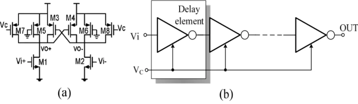
3. Differential voltage-controlled Delay Line
In order to achieve better common-mode noise rejection, the differential delay element has been introduced in [4] as shown in Figure 2.7. The delay element consists of a pseudo differential amplifier for high-speed operation. Since the strong PMOS latch will decrease the bandwidth of the delay cell, the weak PMOS latch, M3–M4, is adopted to speed up the signal transition of the differential pair, M1–M2 .However, it will slow down the slew rate of the output signal. To improve the driving capability of the delay cell, the PMOS transistors, M5–M6 , in triode are added to increase the driving capability. The PMOS transistors, M7–M8, are used to adjust the delay.
Figure 2.7 The DVCDL (a) delay element (b) delay line
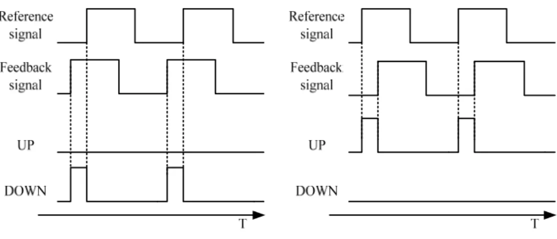
2.2.4 Phase Detector
Phase Detector is a circuit that is response the relationship between reference and feedback signal. Figure 2.8 shows three-state phase detector circuit and Figure 2.9 shows the waveforms in some conditions. Unlike multipliers and XOR gate, three-state PD generates two outputs that are not complementary. When the feedback signal is high and the reference signal is low, then the PD produces positive pulse at down signal, while up signal remains at zero.
Conversely, if reference signal is high and feedback signal is low then positive pulses appear at up signal while down signal is zero. It should be note that, in principle, up and down are never high together in the simulation. The average value of up-down is an indication of phase difference between reference and feedback clock.
Figure 2.9: PD responses with (a) reference signal lag feedback signal (b) reference signal lead feedback
The delay time to reset all internal nodes limits the maximum operation frequency of the phase detector. Therefore, a dynamic phase detector [] is proposed to solve this problem as shown in Figure 2.10. The phase detector is composed of two half-transparent (HT) registers. Due to symmetry of circuit and only three gate delay of critical path, this phase detector has less phase offset and can be operated at a higher frequency than the conventional phase detector.
Figure 2.11: PD state diagram
In the Figure 2.11, it shows the PD circuit behavior. It has three state diagrams: UP=1, DOWN=0 (state 1), UP=0, DOWN=0 (state 0), UP=0, DOWN=1 (state 2). Because the PD is build up from two edge-triggered sequential circuits, we can avoid dependence of the output upon the duty cycle of the inputs. Suppose the circuit is initially in state 0. Then a rising edge on reference signal takes the circuit to state 1, where UP=1, down=0. With state 1 is reached, any more rising edges at reference signal won’t case state change at all. The circuit will remain in this state until a transition occurs on feedback signal, upon which the PD returns to state 0. The switching sequence between state 0 and state 2 is similar. The three-state PD can nominally detect a full range of phase difference, i.e. +2pi,-2pi. A phase difference larger than 2pi is truncated with respect to integer of 2pi. The output of the PD can drive charge pump to produce a controlled voltage for delay line. The charge pump and loop filter will be discussed followed.
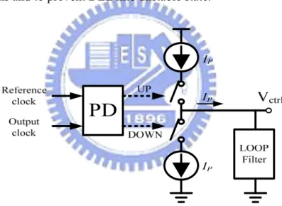
2.2.5 Charge Pump and Loop Filter
The simple model of charge pump and loop filter is shown in Figure 2.12. It consists of two matched current sources and function as switch. When the up signal is
when the down signal is high, the down signal turns on the lower switch and discharges the output node Vctrl. Finally, if both up and down signal are low, then net current is zero and output node Vctrl holds the original voltage. Figure 2.13 shows the simplified timing diagram of charge pump.
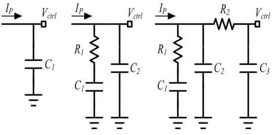
The loop filter can be either passive or active. In general, a passive filter is simple to design and has better noise performance. The passive filter was shown in Figure 2.14, which may be first-order, second-order, or other high order structure. High order filters take advantages of rejecting out-band noise. However, low order filters result in more stable operations. The choice between high order filters and low order filters depends on the applications and to prevent DLL into unstable state.
Figure 2.12: Simple model of charge pump and loop filter
Figure 2.14 Loop filter
2.3
D
IGITALD
ELAY-L
OCKEDL
OOPO
VERVIEWFigure 2.15 Block diagram of digital DLL
As the era of System-On-Chip (SoC) coming, people give more attention on digital DLLs since they are easy to port to different process. Recently, due to the fuel crisis, a power-saving issue becomes more and more important. The power of CMOS circuit is determined primarily by equation P=CFV2, which decreases quadratic ally
with supply voltage. For this reason, the digital DLLs have better power-saving performance since it can operate at lower voltages than analog DLLs.
The conventional digital DLL block is shown in figure 2.15. It consists of three major blocks. They are phase detector (PD), control unit (CU) and digital control delay line (DCDL). The PD detects the phase error between the input clock and the output clock and generates signal to the CU. The CU adjusts the delay line making input clock and output clock in-phase.
We classify four major types of digital DLLs; they are register-controlled, counter-controlled, successive approximation register-controlled, and time measurement controlled DLLs. The following section will describe in detail.
2.3.1 Register-controlled DLL [5]
Figure 2.16 Register controlled DLL
Figure 2.16 shows the block diagram of register-controlled DLL. The n-bit shift register controlled by the output of phase detector. At any time, only on bit of the shift register is active to select a specify delay time of delay line. The phase detector detects the relation between input clock and output clock, and generates left and right signal for shift register to control the amount delay time. When Enable is active, it will enable the shift register, vice versa. The detail operation is described as following. When the
output clock leads the input clock, the phase detector sends left signal to shift register and the high bit in the shift register will be shifted left to increase the delay time to compensate for the delay mismatch. Similarly, when the right is active, the high bit in the shift register will be shifted right to decrease the delay time. When Enable is active, the phase error between the input clock and the output clock is within one unit delay, and the data in the shift register will be held. Under this mechanism, the loop is locked and the phase error will not exceed the unit delay.
Although the control mechanism is quite sample, but when the operating range is increased, the additional delay stages of delay line should be added. Thus, it increases the chip area and power consumption. Beside, the control mechanism is one by one, which means, the more delay stages needs more shift registers to control the delay line. Thus, it also increases locking time. In the worst case, n-bit shift register needs n/2 locking cycles.
2.3.2 Counter-controlled DLL [6]
Basically, the operating principle of counter-controlled DLL is similar to register-controlled DLL expect the up/down counter substitutes for the shift register to control the delay line. In addition, the binary-weighted delay line is adopted and no longer consists of delay stages with equal delay time. Figure 2.17 shows the block diagram of counter-controlled DLL. The active of up/down counter is base on the output of phase detector. The n-bit control word determiners whether the input signal goes through the delay path or passes it. The most different between register-controlled DLL (RDLL) and counter-controlled DLL (CDLL) is area requirement. For example, compare with the RDLL, if 128 delay stages are required in a RDLL, only 7 delay stages are required in a CDLL. Besides, the 128-bit shift register in a RDLL can be substituted for 7-bit up/down counter. While the operating ranges and delay resolution of RDLL and CDLL are the same, the delay line of RDLL will get larger offset delay time and occupy larger chip area than the CDLL. By using CDLL, the chip area could be reduced while maintaining the same operating range as in a RDLL. However, the CDLL still use to linear approach manner to trace the input clock, thus the locking time of CDLL would not get any improvement as RDLL. In the worst case, with n-bit binary-weighted delay line, the locking time maintains n/2 locking cycles.
2.3.3 Successive Approximation Register-controlled DLL [7]
The locking time is an important parameter for digital DLL to evaluate the performance, especially in the high-speed memory applications. The DLLs that mentioned above based on the linear search exhibit the same lock time. The linear search algorithm; however, increases the locking time when frequency is wider. The binary search algorithm may be a better method to reduce the locking time. Figure 2.18 shows the block diagram of binary search (SAR) DLL.
First, the most significant bit (MSB) of the control word is set to 1, and the other bits all are set to 0. The phase detector judge whether the output clock leads the input clock or not. If output clock leads the input clock, the MSB is set to low. If output clock lags the input clock, the MSB remains high and held constant. In this way, the MSB is determined. The operating produce is repeated for the following bit until the least significant bit (LSB) is determined. Figure 2.19 shows an example of the 3-bit binary search algorithm. Assume the final control word is set to “001” and the initial control word is set to “100”. In this example, the output clock leads input clock in the step 1 and step2, and output clock lags input clock in the step 3. Finally the binary searching finds the correct control word “001”.
The SAR DLL is not only reduces the chip area but also shorten the locking time. In the worst case, with n-bit delay line, the locking time of SAR-DLL is log2(2^(n-1)). Unfortunately, The SAR controller in the DLL determines the value of each bit of the word in a sequential and irreversible. Therefore, it becomes an open-loop type circuit after lock-in and never against the PVT variation. An improved SAR DLL [8] was proposed to solve this problem by using the counter-controlled control word instead of SAR-controlled. The initial control word of the counter is load from the SAR controller, and then a counter-controlled DLL is started to maintain the environment variation.
2.3.4 Time measurement controlled DLL
Figure 2.20 TMDLL
Another mechanism to reduce the locking time was proposed in [9] as shown in Figure 2.20. The time measurement controlled DLL divide the locking produce into two stages, coarse tuning and phase tracing. The coarse tuning stage is based on the time to digital converter (TDC) circuit as shown in Figure 2.21. The TDC is used in ADPLL or ADDLL to convert timing information directly to the digital code. The TDC usually consist of the delay that is identical or multiple or fractional to the single delay
cell in the delay line or oscillator, the concept is let timing signal to pass this delay then extracting the information to the digital code.
Figure 2.21TDC circuit
In RDLL and CDLL, the narrow tuning step causes the long locking time. The TDC can measures the input clock period and convert it to digital signals within two clock cycles, then transfer the digital control word to the control block, therefore, the tuning step is extensive. After the coarse tuning stage, the phase tracing stage is active to fine tune the delay of the delay line. Usually, only few control bits need to be determined in the phase tracing stage, therefore, a counter-controlled based control block is preferred. Compare with the TD-DLL and SAR-DLL, there is no different of locking time in phase tracing stage, the most distinction between TD-DLL and SAR-DLL is in the coarse tuning stage. The locking time in the coarse tuning stage of SAR-DLL depends on how many control bits need to be determined, but the TD-DLL can achieve coarse truing within only few cycles. In the worst case, assume m fine tuning bits, the locking time of TD-DLL is (m/2+2) locking cycles. Although the search time of TD-DLL is quite quick, the drawback of TD-DLL is still the area requirement.
2.4
C
LASSIFICATIONS OFD
IGITALLYC
ONTROLLEDD
ELAYL
INEDigitally controlled delay line (DCDL) is the key component of ADDLL. Like most voltage controlled delay line (VCDL), the DCDL consists of several different digitally controlled delay elements (DCDE). The most common delay time adjustment is usually realized by a path-selection approach as shown in Figure 2.22 [10]. In this example, 2n delay buffer are connected in series. A decoder decodes an n-bit control word D into 2 n control lines. Hence, if the propagation delay time of each buffer stage is Tbuffer, then the time resolution is 2*Tbuffer.
There are other architectures that have been used to implement a DCDE. In the following section, we will introduce different kinds of DCDE.
Figure 2.22 DCDL realized by a path-selection method
2.4.1 Shunt Capacitor based DCDE
Figure 2.23 shows the basic circuit of using a shunt capacitor based DCDE [11]. In this circuit, MC1~MCn acts as shunt capacitor. Transistor M1~Mn controls the charging and discharging current to the MC1~MCn. The operating is similar to RCCDL; replace the Vctrl to the digital control word D which is n-bit resolution controls the
equivalent capacitance on the output node. As a consequence, the delay time of shunt capacitor based method can be controlled in binary-weigh. The drawback of shunt capacitor based DCDE is sensitive to power supply noise and PVT variation.
Figure 2.23 Shunt-capacitor based DCDE
2.4.2 Standard Cell based DCDE
One simple example of standard cell based DCDE was proposed in [12], as shown in Figure 2.24. The delay element is cascaded six inverters in the first row and the additional tri-state inverter with its control bit is added in every column. By enabling the number of tri-state inverter buffer, the delay time of DCDE can be controlled. It is simple and easy to implement. However, it needs large area and high power dissipation for the fine tune necessarily in the DCDL design. Besides, the resolution is hard to be uniform.
Figure 2.24 Parallel tri-state inverter based DCDE
The other example, as shown in Figure 2.25, the DCDE is implemented by an add-or-inverter (AOI) cell and or-and-inverter (OAI) cell with two parallel tri-state inverters was proposed in [13]. The basic method is to adjust the driving capability with resistance control. The advantage is that this fine tune method of DCDE has less area and power dissipation compare with [12]. However, since it’s based in AOI-OAI cell to change the delay resolution, the resolution step is also hard to be uniform and sensitive to power-supply variation. Besides, it also requires an additional decoder for mapping the control input of AOI-OAI cell.
Due to inherent drawbacks of cell-based delay cell, such as finite resolution and nonlinear delay versus control words, the novel delay cell is proposed in [13] to improve delay resolution and monotonic delay behavior with respect to digital control codes. Figure 2.26 (a) illustrates a novel delay cell using a two-input NOR gate. The delay method is to give node’D different digital signal since total gate capacitance of transistors M2 and M3 varies with different voltage of node’D. Figure 2.27 compares the delay resolution between [12] and [13], showing that the novel delay cell [13] has better linearity than OAI cell in [12].
Figure 2.26 (a) Circuit with digital control. (b) Equivalent circuit with _C capacitance.
2.4.3 Low power DCDE
The low power DCDL named binary-weighted differential-delay cells (BWDC) is proposed in [14], as shown in Figure 2.28. In BWDC, one path comprises of a fixed capacitance realized with the minimum-sized transistor and the other path comprises of a tuning capacitance that is realized by adjusting the size of transistor. The difference of capacitance determines the finest delay resolution, which can be made sufficiently small. The BWDC also has two distinct features that contribute to low power. First, there is no need for large driving and so logic gates can be minimally sized. Second, the de-multiplexing gates are placed at the input side so that only the components in one path are activated.
Figure 2.28: The binary-weighted differential-delay cell.
2.4.4 Current-starved based DCDE
The current starved based DCDE was proposed in [15]. As Figure 2.29 shows, the charging and discharging currents of the inverter, composed of M1 and M2, are controlled by two sets of current-controlling nMOS (Mn0, Mn1, …) and pMOS (Mp1, Mp2, …) transistors at the source of M1 and M2, respectively. The current controlling transistors are sized in a binary version to allow binary-weighted delay time. By
applying a specific binary vector to the controlling transistors, a combination of transistors is turned on at the sources of M1 and M2 transistors. Such an arrangement controls the rise time and fall time of the output voltage of the inverter.
However, one of the problems with the current staved based DCDE architectures is the non-monotonic delay behavior with ascending binary input vector. The input vector changes the effective resistance of transistors placed at the source of the nMOS or pMOS transistors of the inverter. This not only changes the resistance at the source of M1 or M2, but also changes the parasitic capacitance associated with transistors at these nodes. This is because the parasitic capacitance at the drain of a MOSFET is different in the ON and OFF states.
Figure 2.29 Current starved based DCDE
In [16], there are two factors depending on the input vector to affect the delay : (1) The resistance of the controlling transistors:
The circuit delay can be increased / decreased by increasing / decreasing the effective ON resistance of the controlling transistors at the source of M1.
(2) The capacitance of the controlling transistors:
the overall delay decrease as the effective capacitance of the controlling transistors at the source of M1 increase. The larger resistance increases the delay; however, larger parasitic capacitance decreases the delay. The effective capacitance seen at the source of M1 depends on which controlling transistors are on. Because of the ON and OFF capacitances between drain and ground of a MOSFET is different. Therefore, it may make monotonic characteristic of the DCDE can not be ensured with ascending input vector. This situation will be further complicated as the number of delay controlling transistors increases. Table 1 shows the comparison of the different type of DCDE.
Table 1 Comparison of different type DCDE
Delay cell type
Drawbacks Circuit
structure
Shunt-capacitor based
¾ Sensitive to power supply noise
¾ Process mismatch
Standard-cell based
¾ Larger area and power dissipation
¾ Delay resolution
¾ Different coarse delay and fine delay cells
Low power DCDL
¾ Intrinsic delay time as delay cell cascaded
Current-starved based
¾ Sensitive to PVT variation ¾ Poor linearity
2.5
C
OMPARISON OFD
IFFERENTT
YPESO
FDLL
SFinally, comparison of different types of DLLs is given in Table 2
Table 2 Comparison of different types DLL
Analog DLL Mixed-mode DLL Digital DLL
Design cycle Slow Slow Fast
Noise rejection Poor Poor Good
Resolution High High Low
Lock time Slow Middle Fast
Area Large Large Small
CHAPTER 3
MULTIPHASE DLL AND DLL-BASED
FREQUENCY MULTIPLIER
3.1
I
NTRODUCTION OFM
ULTIPHASEDLL
A ring-oscillator-based phase locked loop (PLL) or delay line based delay-locked loop (DLL) has been widely used because they have ability to generate multiphase clock signals. The multiphase clock signals can be used in various applications such as time-interleaved architectures, transmitter and receiver [9], and high speed IO. In wireless communication systems, the multiphase clock signals are easily converted into the in-phase and quadrature (I/Q) signals with π/4 radian difference essential for the down-conversion mixer [24]. In frequency synthesizer, the multiphase DLL can combine each phase and generate a high frequency signal [20].
3.2
A
PPLICATION OFM
ULTIPHASEDLL
In this section, we will introduce the application of multiphase DLL in detail. In these applications, the multiphase DLL is used to replace the PLL due to their ease of design, better immunity to on-chip noise, and no jitter accumulation characteristic.
3.2.1 DDR SDRAM Controller Application [17]
In Double Data Rate (DDR) SDRAM controller design, output data strobe (DQS) signal must be delayed by a fixed timing delay (tSD) to capture the output data (DQ) correctly. Figure 3.1 shows this read operation timing budget. Ideally, the DQS and
DQ is edge aligned by DDR SDRAM. However due to pin-to-pin skew among all DQ and DQS, and PCB board skew, the data valid window becomes smaller than expected. The calculations for timing budget show that the optimal value for tSD is approximately 20 percent of an input clock period. Since the input clock frequency range from 100MHz to 200MHz (DDR-200/266/333/400), the tSD value varies from 2ns (=10nsX0.2) to 1ns (=5nsX0.2). Therefore, a five-phase all-digital DLL is proposed to generate the desired tSD delay for DQS signal.
Figure 3.1 Read operation timing budget
The block diagram of the five-phase all-digital DLL for a DDR SDRAM controller application is shown in Figure 3.2. Like most of DLL-based multi-phase clock generators, the DLL has a multi-stage delay line with the same control word to generate equally spaced multi-phase clock output. It uses the time-to-digital (TDC) scheme to lock whole loop. Hence, a design consideration should be noticed is that sometimes it is difficult to meet the minimum delay constraint when using standard cell to build up a high resolution delay cell. Therefore, the DLL in this design is lock to two periods of the reference clock period by using TDC scheme. After DLL is locked, the phase spacing of each delay stage should be 2*T /5, where T
means the clock period of the reference clock. Hence the minimum delay constraint for each delay stage is extended twice as original. The total delay from DQS to DQSD becomes 1.2xTFREF, which means the phase shift between DQS and DQSD is still 0.2xTFREF. As a result, the desired tSD delay can be generated by the multiphase DLL.
3.2.2 Transmitter [9]
In digital communication applications, the multiphase DLL is applied to a data cannel compression transceiver. The architecture of the transceiver is shown in Figure 3.3. The transmitter’s output, TX_DATA and TX_CLK, are sent to the receiver’s inputs, RX_DATA and RX_CLK, respectively. In the transmitter, the generated seven-phase clock signals are used to transfer 7-bits data (DATA [6:0]) into one data channel (TX_DATA), and the TX_CLK is also sent to the receiver. The “TX delay mirror” shown in Figure 3.3(a) is used to compensate the delay time of the parallel-to-serial converter. The receiver shown in Figure 3.3 (b) recovers the received data stream (RX_DATA) back to original 7-bits data (DATA_OUT [6:0]). The two-phase ADMCG shown in Figure 3.3 (b) is used to estimate the accurate delay of TREF/14. It aligns two adjacent phases of the seven-phase DLL outputs (i.e., P6 and P0) to measure the delay, and the received data stream will first be delayed by and then sampled by the seven-phase multiphase clock signals. Thus, those multiphase clock signals can sample the received data stream in the center of the bit symbol boundary, and this maximizes the timing margin of the receiver circuit.
3.2.3 High-performance Microprocessors [18]
Execution engines of multi-gigahertz superscalar processors require multiphase clock signals with accurate edge-position to trigger dynamic data path circuits. The intermediate clock phases need automatic stretch ability in proportion to the core clock period. Moreover, multiphase clock can also be used in large SoCs to achieve a higher operating speed than the main internal clock frequency. Figure 3.4 shows the organization of the multiphase clock generator for high-performance microprocessors. This multiphase clock generator has several features:adopts a closed-to-open loop control scheme with a jitter-averaging counter to combine the benefits of both fixed/programmable delay-lines and digital DLL-based techniques, thereby achieving high resolution, flexibility, andfrequency-range.
3.3
I
NTRODUCTION OFDLL-B
ASEDF
REQUENCYM
ULTIPLIEPLL-based frequency synthesizer has been widely used until recent times. Another type that draws attention is DLL-based frequency synthesis. DLL-based frequency synthesizer takes advantage of low phase noise since they derive the output signal directly from a clean crystal reference which has low noise accumulation. Moreover, the DLLs can be designed as a first-order system to allow a wider loop bandwidth and settling times on the order of nanoseconds, which are particularly suitable for applications where fast-lock issue is required, such as ultra-wide band system.
3.3.1 Basic of the DLL-Based Frequency Multiplier
Conventional DLLs can not generate different frequency of input clock frequency. However, by using the edge combiner and replacing voltage-controlled oscillator (VCO) with delay line, a DLL can operate as PLL. The simplified block diagram of DLL-based frequency synthesizer is shown in Figure 3.5. When the loop is locked, the output phases of every delay stage are evenly spaced one reference clock period Tref. Each phase difference of two delay stage has a delay of Tref/N. Then, the edge combiner can generates a transition for each phase output transition; hence, the output frequency is N times the reference frequency Tref. The operation diagram is illustrated in Figure 3.6.
Figure 3.5 Organization of the multiphase clock generator.
Figure 3.6: Operation timing diagram of frequency multiplier
3.3.2 Timing Jitter Accumulation [19]
A DLL-based frequency using a voltage-controlled delay chain has an inherent advantage over a PLL using a voltage-controlled oscillator. Figure 3.7 shows timing jitter accumulation for an oscillator compared with that of a DLL-based frequency multiplier. In an oscillator, random timing errors accumulate because the timing jitter at
the end of each oscillation is the starting point of the next. The random timing error of the output signal is the sum of the timing errors of all previous oscillations. This translates to a poor long-term jitter performance, or, equivalently, poor close in phase noise. Figure 3.7 shows the random timing uncertainty for a ring oscillator increase as a function of time.
Figure 3.7 Timing jitter accumulation for ring oscillator and delay chain.
In contrast, for a finite length delay line in the DLL-based frequency multiplier, the random timing error accumulates only within a single delay chain cycle. The timing error in one cycle of the delay chain does not affect the next cycle, because the waveform that triggers the next output oscillation is the reference clock waveform. This provides excellent long-term jitter performance, or, equivalently, a low close-in phase noise. The different phase noise signatures of a PLL with a VCO and a DLL-based frequency multiplier can also be understood by examining the source of synthesized output waveform. In a PLL, the output signal is taken directly from a VCO whose
response of the PLL in which it is embedded. However, the PLL bandwidth is constrained by practical considerations to a value several orders of magnitude lower than the output frequency. In contrast, each output edge from the DLL only contains the timing uncertainties accumulated from the previous delay stages within the same reference oscillation period. Limited jitter accumulation gives a flat phase noise profile for offset frequencies less than f
ref. The long-term timing error accumulation, equivalent to the close-in phase noise, is much lower than that of a typical VCO.
3.4
A
PPLICATION OFDLL-B
ASEDF
REQUENCYM
ULTIPLIERecently, DLL-based frequency multipliers are used in communication system applications, high speed IO due to its low phase noise. In this section, we will introduce several DLL-based frequency multiplier architectures and its applications.
3.4.1 Local Oscillator for PCS Application [20]
Figure 3.8 shows the DLL-based frequency multiplier for PCS application. The objective of the DLL-based frequency multiplier is to produce a low-phase-noise RF signal by taking advantage of the inherently low jitter of a low-frequency crystal oscillator reference. As shown in Figure 3.8, the reference crystal signal is first amplified and drives the delay chain. The delay chain consists of nine delay stages and is locked to half of the reference crystal period. A phase detector, charge pump, and loop filter are used to create the control voltage for the delay chain. The edge combiner combines all the outputs from the DLL and creates the multiplied frequency.
Figure 3.8 Block diagram for the experimental prototype
The edge combiner consists nine NMOS input differential pairs and a pair of LC-tanks and is similar to the folding amplifier as shown in Figure 3.9. The DLL have an odd number of delay element, and a single current is modulated back and forth between the LC-tanks to create the multiplied frequency. However, the multiple factor is fixed, and LC-tanks occupy a lot of chip area, which is not suitable for SoC design.
3.4.2 A Multiplying DLL for High Speed On-chip Clock
Generation [21]
As bandwidth demand of computer and digital communications components continues to grow, high-speed serial I/O links are replacing traditional parallel buses. Operating at speeds of up to 5 Gb/s, such high-speed I/O circuits are already found in packet switches, circuit switches, and processor- memory interconnects. Figure 3.10 shows the high-level diagram of high speed serial I/O consisting of a serializing transmitter, a channel, and a desterilizing receiver. To operate with a bit period that is small compared to the time-of-flight over the channel, high-speed I/O circuits are typically terminated with a matched impendence at either or both ends to achieve incident-wave signaling and recover the clock phases from the data arriving at the receiver. A major timing noise contributor in high-speed I/O systems is the clock multiplier, which takes a low frequency and in most case, accurate reference clock and synthesizes a high frequency timing reference for the bit stream.
The multiplying DLL architecture is shown in Figure 3.11. This circuit accepts an input clock and generates a phase-locked output clock at a multiple of the input clock frequency. As with a DLL, each rising edge of the input clock zeros the phase error of the loop. Hence this circuit combines the low phase noise of a DLL with the clock multiplication ability of a PLL. Because the same delay elements generate each edge of the output clock in an MDLL, the fixed-pattern jitter due to device mismatch in a conventional DLL frequency synthesizer is eliminated.
Figure 3.10 Basic components of a high-speed serial I/O
Figure 3.11 Multiplying DLL
3.4.3 Clock Generator for Dynamic Frequency Scaling
In recent years, power consumption has become a critical issue in the embedded systems, especially for the mobile systems. A dynamic Voltage Frequency Scaling (DVFS) becomes more important for saving energy on mobile embedded systems. A DVFS scheme is also proposed in [22]. A frequency adjuster circuit unit calculates the
monitor to reserve the required number of inactive margin cycles within the monitoring period and indicates the next clock frequency to the clock generator. The dynamic frequency is selected by the clock thinning circuit which collects several different frequency input. Therefore, it can operate continuously without PLL relock or system.
Figure 3.12 shows the power consumption comparison between using DVFS and without using DVFS. In MPEG4 application, power consumption reduces 72%; on the other hand, power consumption reduces 83% in PIM application. It is clear that DVFS can save energy significantly.
Figure 3.12 Comparison of power consumption
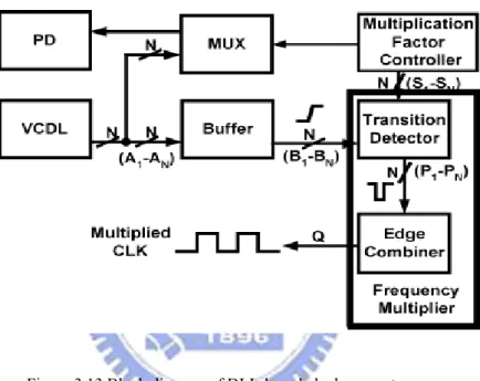
In order not to make performance overhead, the relock time is an important issue for the DFS. A multiphase DLL based clock generator which has fast relock time is proposed in [23]. Figure 3.13 shows the DLL based clock generator block diagram. If the VCDL has N delay cells, then the output frequency can be expressed as equation (1), where Freq_Output CLk is frequency of the reference signal and the multiplication factor M/2 can be chosen dynamically by the multiplication factor controller. The digital logic
transition detector and edge combiner is for frequency adjustment, the multiplication factor can be changed with fast lock time. For the specific case, it only takes one-cycle to lock during frequency scaling.
CHAPTER 4
A WIDE POWER SUPPLY RANGE,
WIDE LOCKING RANG ALL-DIGITAL
MULTIPHASE DLL
In this chapter, an adaptive SAR (ASAR) search algorithm is proposed to achieve fast lock time and extend the locking range. The ASAR search algorithm is based on the frequency-estimation selector and SAR controller, which is designed in digital mode. Compare with the conventional counter-controlled DLL (CDLL), successive approximation register-controlled DLL (SARDLL), and variable SAR DLL (VSARDLL), the ASAR-based DLL can avoid harmonic locking in wide-locking range. Moreover, the ASAR-controller is designed in the robust and low power flip-flop, which is suitable for the wide power supply range operation.
4.1
I
NTRODUCTION OFW
IDE-R
ANGEDLL
Phase-Locked loops (PLL) and delay-locked loops (DLLs) are widely used as de-skew buffers in microprocessors, memory interface, and communication products. Generally, in several high performance applications, such as double date rate (DDR) SDRAM [17], clock data recovery (CDR) [25], and multi-core processors [26], multiphase DLLs (MDLLs) are often preferred due to their better performances of jitter, stability, and simple design effort than PLLs.
Recently, as the need of wide operating frequency range increasing, conventional MDLLs may suffer from harmonic lock issue. Figure 4.1 shows the harmonic locking
problem [27].In the DLL, the reference clock, ref_clk, is propagated through VCDL. The output signal, vcdl_clk, at the end of the delay line is compared with the reference input. If delay different from integer multiples of clock period is detected, the closed loop will automatically correct it by changing the delay time of the VCDL. However, the conventional DLL will fail to lock (case 3) or falsely lock to two or more periods (case 4), Tclk, of the input signal if the initial delay of the VCDL is shorter than 0.5*Tclk or longer than 1.5*Tclk. Therefore, if the DLL is required to lock the delay to one clock cycle of the input reference signal, the initial delay of the VCDL needs to be located between 0.5*Tclk and 1.5*Tclk as (case 1 and case 2) shown.As a result, the additional circuit or control mechanism is needed to avoid the false lock. In the next Section, we will introduce the previous research of wide range scheme.
4.2
P
REVIOUSR
ESEARCH OFW
IDE-R
ANGEDLL
Various wide-range DLLs have been proposed in [8] [28] [29] [30] to solve the harmonic lock problem. In [8], an all-analog DLL uses the replica delay line is proposed to solve the narrow operating frequency range problem of a conventional DLL. The auxiliary loop uses a replica delay line to extend the main loop locking range, as shown in Figure 4.2. If the delay range of the VCDL satisfies the relation TVCDLmin <1/7×TVCDLmax, the DLL will have a maximum operation range of 7:1. However, the process-sensitive characteristic makes the analog DLLs difficult to migrate to advanced technologies Therefore, digital DLL is developed to improve process portability.
Figure 4.2 Configuration and operation of a replica delay line.
A digital-controlled DLL called the self-correcting DLL is proposed in [30]. The problem of false locking is solved by the addition of a lock-detect circuit and the modified phase detector (PD) as shown Figure 4.3. The modified PD decodes each clock phase and sends over and under signal to avoid harmonic locking, the waveform is shown in Figure 4.4. Although this self-correcting DLL avoids false locking, the outputs of the VCDL are required to have an exact 50% duty cycle.
Figure 4.3 (a) Lock-detect decode circuitry (b) Phase detector schematic
Figure 4.4 Nine-stage VCDL waveforms with (a) correct lock and (b) false lock
The time-to-digital (TDC) scheme may be the simplest concept to resolve the harmonic problem. In [9], the multiphase clock generator is used to overcome the false locking problem. The TDC circuit measures the period of the input clock directly and converts the timing information to digital signals and controls the delay time of the delay line to avoid false locking. However, such DLLs result in complex architectures that face such problems as increased area, increased power consumption. Figure 4.5 shows the simplify TDC architecture.
Figure 4.5 The TDC architecture
The variable successive approximation register (VSAR) algorithm is proposed in [8] for all-digital DLL applications. The main control unit is composed of conventional SAR units, variable SAR units and fail-to-lock judgment circuit (FJC). Initially, the conventional SAR units borrow one bit as a MSB form the LSB of variable SAR units to perform a binary search. After the binary search is finished, the FJC examines the lock state. When the locking produce is fail, the conventional SAR units borrow one more LSB from the variable units and repeat the locking produce. Before the total number of borrowed bits is reached, the locking produce repeats until the DLL is locked correctly. Once the lock state is confirmed, the control unit is transformed into a counter for a closed-loop operation. For the variable SAR algorithm, the delay of delay line increases gradually from the minimum and never exceed twice of the input clock period. Therefore, the harmonic locking problem can be avoided. The flowchart of the VSAR algorithm and controller are shown in Figure 4.6
Figure 4.6 (a) The flowchart of the VSAR algorithm (b) VSAR controller
In comparison with the conventional SAR algorithm, the variable SAR algorithm has two advantages: (1) it varies from the open-loop characteristic of conventional binary search algorithm to the close-loop type. (2) The division ratio (DR) based on the variable SAR algorithm can be the minimum of two. Therefore, the variable SAR algorithm can accelerate the locking time and avoid harmonic locking in wide-frequency range. Compare with conventional SAR, up to 7X speedup can be achieved; the simulated lock time versus the operating frequency is shown in Figure 4.7. However, the most drawback of the variable SAR algorithm is still complex hardware required and more power consumption
4.3
A
DAPTIVESAR
A
LGORITHMThe design challenges of the lock-in controller include lock time, locking range, and area requirement. In order to balance these considerations, a SAR lock-in controller [7] may be the most suitable for all-digital DLLs. However, the conventional SAR controller has harmonic locking issue in wide frequency range, which is not allowed in multiphase DLL applications. To avoid harmonic locking, the delay line range should be always satisfied equation (4.1) [29]
DCDL_MIN DCDL_MAX
REF DCDL_MAX DCDL_MIN
2
(T
,
T
)
3
T
(T
,2 T
)
(4.1)
Max
MIN
×
<
<
×
where TREF means the reference clock period, TDCDL_MIN means minimum delay time of the delay line, and TDCDL_MAX means maximum delay time. For the conventional SAR algorithm, the initial delay time is always set in the middle of delay time as (TDCDL_MIN+TDCDL_MAX)/2. Thus, substitute this condition into equation (4.1), the locking of range conventional SAR algorithm is limited to (4.2).
DCDL_MAX DCDL_MIN) Target DCDL_MAX
(T
+ T
) / 3 T
<
<
T
(4.2)
Equation (4.2) shows that though SAR algorithm has fast locking time, it will fail to lock in wide frequency range without any auxiliary hardware.
The proposed adaptive SAR strategy is using the frequency-estimation selector (the circuit is described in next section) to pre-obtain approximate input frequency range and generates digital codes (S1, S0) to adaptive SAR controller. Meanwhile, the adaptive SAR controller utilizes the codes (S1, S0), giving the multiphase DLL proper initial delay to avoid false locking. For example, if input frequency is high, the LU starts with shorter binary-weighted initial delay, like one-quarter delay time of the delay
line instead of always choosing in the half. In our adaptive SAR controller, we provide three different initial delay of delay line: one-half, one-quarter, and one-eighth, as shown in Figure 4.8. Consequently, the locking range of the proposed adaptive SAR algorithm can be extended as
DCDL_MAX DCDL_MIN) Target DCDL_MAX
(T
+ T
) /12 T
<
<
T
(4.3)
From equation (4.3), the proposed adaptive SAR strategy theoretically has maximum locking range when TDCDL_MAX = 11x TDCDL_MIN. Hence, the locking range can be extended from two times to one order, comparing with conventional SAR search. To prevent the false locking caused by PVT variations, the locking range should be overlapped pair-wisely.
Compared with previous research in [1][8][9][29], which require replica delay or complex control circuit, the adaptive SAR strategy has three features: (1) it reuses the delay line to perform time measurement to avoid false lock; therefore, the circuit area and power consumption are significantly reduced; (2) input duty cycle immunity, since it samples two times period of reference clock as frequency measurement. (3) operate in digital mode, which is robust and suitable for wide voltage range operation