國
立
交
通
大
學
物理研究所
碩 士 論 文
刮刀塗佈技術於有機太陽能電池與多層結構有機鄰
近感測器的應用
Blade coating for polymer solar cells and multilayer
polymer photo-detectors
系 所 別:物理研究所碩士班
研 究 生:張玉函 (Yu-Han Chang)
指導教授:孟心飛 教授 (Prof. Hsin-Fei Meng)
洪勝富 教授 (Prof. Sheng-Fu Horng)
刮刀塗佈技術於有機太陽能電池與多層結構有機鄰近感測器的應用
Blade coating for polymer solar cells and multilayer polymer
photo-detectors
研究生:張玉函 Student:Yu-Han Chang
指導教授:孟心飛 教授 Advisor:Prof. Hsin-Fei Meng
國 立 交 通 大 學 物理研究所 碩 士 論 文
A Thesis
A Dissertation Submitted to Institute of Physics College of Science National Chiao Tung University
in partial Fulfillment of the Requirements for the Degree of
Master in Physics June 2009
Hsinchu, Taiwan, Republic of China
刮刀塗佈技術於有機太陽能電池與多層結構有機鄰
近感測器的應用
國立交通大學物理研究所碩士班
學生:張玉函 指導教授:孟心飛 教授 洪勝富 教授摘要
本研究採用施子(donor)材料- poly(3-hexylthiophene) (P3HT)以及受子(acceptor)材 料-(6,6)-phenyl-C61-butyric acid methyl ester (PCBM),將其均勻混合於甲苯(toluene)溶 液,利用刮刀塗佈技術製作塊材異質接面有機太陽能電池與光感測器。利用刮刀塗佈 製程使能夠有序排列形成施子-受子的自組裝結構以提升載子的傳輸效率。
本研究之有機太陽能電池達到高能量轉換效率(power conversion efficiency, PCE) 3.8%,相較於一般於甲苯溶液以旋轉塗佈(spin coating)製程效率 2.6%,整體元件效益 提升達 46%。於光感測元件的研究,透過刮刀製程應用於多層結構設計,將元件暗電 流密度降低至 10-5 mA/cm2,比單層旋轉塗佈製程元件可降低其暗電流值的 100 倍,有 效提升整體元件感測靈敏度。 關鍵字:共軛高分子、塊材異質接面、太陽能電池、光偵測器、P3HT、PCBM
Blade coating for polymer solar cells and multilayer
polymer photo-detectors
Institute of Physic
National Chiao Tung University
Student: Yu-Han Chang Advisors: Prof. Hsin-Fei Meng
Prof. Sheng-Fu Horng
Abstract
A donor-acceptor blend for bulk hetero-junction polymer solar cells and polymer photo-detectors are studied by using poly(3-hexylthiophene) (P3HT) as the donor and (6,6)-phenyl-C61-butyric acid methyl ester (PCBM) as the acceptor. Desired ordered donor-acceptor self-organization is achieved by blade coating with high carrier mobility.
The polymer solar cell with power conversion efficiency (PCE) is 3.8% in this study, which is 46% higher than that obtained by spin coating in toluene solution (2.6%). In addition, the multilayer photo-detector can be achieved by blade coating to reduce dark current density to 10-5 mA/cm2. That is about 100 times lower than that of single layer structure by spin coating, enhancing the sensitivity.
Key word: conjugate polymer, bulk hetero-junction, polymer solar cell, polymer
致
謝
悄悄的我走了,正如我悄悄的來; 我揮一揮衣袖,不帶走一片雲彩。 猶記得第一次細讀這首耳熟能詳的「再別康橋」,腦海中盪漾著〝不帶走一片雲 彩〞如此的告別多麼灑脫自得!作者寄情於康橋景致的離情依依,給了我無限的感動! 回顧研究生涯兩年來的時光,腦海中的回憶如相片膠捲般一幕幕浮現,實驗室這個大 家庭幾乎是這些年來研究生活的全部,精采的故事很多,一起難過、一起歡笑的畫面 至今仍記憶猶新。離別的時刻,由衷地感謝每一位陪伴我一路走來的師長與好友,此 刻帶走的是各位給我的一片情誼! 首先感謝的是實驗室兩位大家長 孟心飛教授和 洪勝富教授,感謝兩位老師在研 究道路上指引我重要的方向。特別是我的指導教授-孟老師,還記得放榜之際第一次邀 請您擔任指導教授的場景,如今轉眼我已完成了學業。兩年多來的日子感激老師悉心 的指導並給予我許多的學習機會,養成應有的研究精神與態度,豐富的學習經驗充實 了我的碩士研究生涯。 「有機半導體實驗室」就像個熱鬧的大家庭,在嚴謹的研究要求之下,也不乏許 多開心愉快的氣氛。尤其幾位實驗室重要的博士班學長姊們一直是我學習的好榜樣, 宇強學長、家銘學長、建成學長在研究上總不吝分享豐富的研究經驗,平常也很照顧 學弟妹;明錕學長和仁君學姊在專業研究領域上總熱心給予學弟妹們盡可能的協助; 以及俊宇學長、銘志學長、韻茹學姊平日開心愉快的笑容爲實驗室營造不少輕鬆愉快 的氣氛。 LED組更是這大家庭裡一群令人難忘的家人。兩年來信榮學長就像是LED組一把 穩固的大傘呵護我們在研究之路上一步一步地成長,實驗上實事求是的要求以及親切 耐心的討論分享,從摸索學習到放手讓我們每一個人擁有各自研究領域的一片天。猶記每回小組會議之後一群小毛頭圍著你討論實驗方向的場景,是腦海裡深刻的畫面; 這些年來無限的感激化為一句深深的謝謝你!冠成學長總是細心地給予學弟妹許多的 關心,一路陪伴我們走來,是學長更是知心的好友。恩禎學長就像個鄰家大哥一般, 無論研究上或生活上的事物總樂於與人分享,有你的地方就有歡笑,是我們組內最寶 貝的開心果。還有六年的同窗好友重麟、青春洋溢的紘瑋、活潑搞笑的佳達、貼心好 男人形象的文興、溫柔婉約的季庭、外向健談的勝佳、中肯踏實的嘉佑、對凡事都很 認真的宗祐以及認真上進的碩一學弟韋嵐,多麼難得的緣份讓我們齊聚人生中寶貴的 兩年,因為有你們讓我的研究生活多采多姿,滿滿的回憶裡永遠記得大家燦爛的笑容 與開懷的笑聲。 最後我要感謝我摯愛的家人,視我己出的姑媽 張艾倫女士和伯父 張化民先生, 謝謝你們在我成長過程中無微不至的照顧與關愛。媽媽 陳金貴女士在我求學階段默默 地支持與鼓勵我。很感恩我生長在一個未必健全卻充滿幸福的家庭,因為擁有家人許 多的溫暖讓我即使面對困境也能勇敢的向前走,我愛你們!我是一個幸福的女孩,在 人生的旅程上有著貼心的男友兆仟、知心的好姊妹詩敏,與你們一起,我可以自在地 開心的大笑、難過的大哭,感謝你們始終陪伴著我! 要感激的人真的很多,謝謝老天爺給我雖不富有卻幸福的家庭、雖不完美卻值得 珍惜的人生!畢業是人生一個階段的結束,我將帶著更多的祝福與期望邁向下一個人 生嶄新的新頁。 交通大學物理研究所 張玉函 2009年七月
Contents
摘要 ... i Abstract...ii 致謝 ...iii Contents ... v Tables...viiPart 1 Efficient polymer solar cells by blade coating ...vii
Figures ...viii
Part 1 Efficient polymer solar cells by blade coating
Chapter 1 Introduction... 11.1 Background of research ... 1
1.1.1 Energy resources and solar energy ... 1
1.1.2 Development of solar cells ... 2
1.1.3 Development of polymer solar cells ... 4
1.2 Motivation of research... 8
1.2.1 Opportunity for polymer solar cells... 8
1.2.2 Advantage of blade coating application in polymer solar cells ... 9
1.3 Thesis frameworks for part 1... 11
Chapter 2 Theory ... 12
2.1 Fundamental principles of solar cells ... 12
2.1.1 Equivalent circuit... 12
2.1.2 Basic parameters... 16
2.2 Characteristics of conjugate polymer materials... 20
2.2.1 Development... 20
2.2.2 Photovoltaic property ... 20
Chapter 3 Method ... 23
3.1 Experimental system ... 23
3.1.1 Working principle of blade coating ... 23
3.1.2 Device structures ... 23
3.1.3 Material introduction ... 24
3.2 Experimental process and measurement ... 26
3.2.1 Deposition of the hole transport layer ... 26
3.2.2 Deposition of the active layer... 26
3.3 Measurement ... 27
3.3.1 Photovoltaic property ... 27
3.3.3 Morphology ... 27
Chapter 4 Result and discussion... 28
4.1 Device performance of bulk hetero-junction cells ... 28
4.2 Roughness of net P3HT and PCBM film ... 36
Chapter 5 Conclusion ... 39
Part 2 Multilayer polymer photo-detectors
Chapter 6 Introduction of polymer photo-detectors ... 406.1 Background of research ... 40
6.1.1 Introduction of p`olymer proximity sensors ... 40
6.1.2 Development of polymer proximity sensors ... 41
6.1.3 Introduction of polymer photo-detectors ... 41
6.2 Motivation of research... 43
6.2.1 Problems of polymer photo-detectors ... 43
6.2.2 Multilayer structures... 44
6.2.3 Multilayer structures by Blade coating... 45
6.3 Thesis frameworks for part 2... 46
Chapter 7 Method ... 47
7.1 Material introduction ... 47
7.2 Experimental processes ... 47
7.2.1 Solution preparation ... 48
7.2.2 Deposition of the active layer... 48
7.3 Measurement ... 50
7.3.1 Photovoltaic property ... 50
Chapter 8 Result and discussion... 51
8.1 Single layer structures ... 51
8.1.1 P3HT diode with blade coating and spin coating ... 51
8.1.2 Single layer photo-detector by blade coating and spin coating ... 53
8.2 Multilayer photo-detectors with PCBM as hole blocking layer ... 54
8.2.1 Bilayer structures ... 54
8.2.2 Trilayer structure ... 56
8.2.3 Problems of PCBM layer... 63
8.3 Multilayer structures with BPhen as hole blocking layer... 63
8.3.1 Bilayer structure ... 63
8.3.2 Trilayer structure ... 64
8.3.3 The problem of BPhen layer... 67
8.4 Next improvement ... 68
Tables
Part 1 Efficient polymer solar cells by blade coating
Table 4-1 Performance of bulk hetero-junction solar cells in this work. ... 33 Table 4-2 The roughness of P3HT:PCBM, net P3HT, and net PCBM films... 38
Part 2 Multilayer polymer photo-detectors
Table 7-1 The conditions of the multilayer devices... 49 Table 9-1 The summary of dark current for polymer photo-detector ... 69
Figures
Part 1 Efficient polymer solar cells by blade coating
Fig. 1-1-a The requirement of energy and the tendency several energy decreasing ... 2
Fig. 1-1-b The power conversion rate development of several solar cell types ... 4
Fig. 1-1-c Organic solar cell structures development... 4
Fig. 1-1-d Bulk hetero-junction structure ... 6
Fig. 1-1-e Working principle of dye-sensitized solar cell... 8
Fig. 1-1-f Development table of polymer solar cell ... 7
Fig. 2-1-a The conventional solar cell with the PN junction structure... 12
Fig. 2-1-b Excitons separate by the build-in electric field ... 12
Fig. 2-1-c I-V characteristics curve of the ideal solar cell under illumination ... 13
Fig. 2-1-d Equivalent circuit of the ideal solar cell ... 13
Fig. 2-2-e Equivalent circuit for a real solar cell ... 14
Fig. 2-1-f I-V characteristics curve of the ideal solar cells and the real solar cells under illumination ... 15
Fig. 2-1-g The I-V characteristics curve of a solar cell of (a) different series resistance (b) different shunt resistance... 16
Fig. 2-2-a The relation between the I-V characteristics and the parameter definition of a solar cell ... 17
Fig. 2-2-b The energy band of the material interface and the electrode in short-circuit condition... 19
Fig. 2-2-c The complex degree of the organic material... 20
Fig. 2-2-d Polymer molecular structure of polyacetylene ... 21
Fig. 2-2-d The electronic conduction region of the conjugate polymer with doping ... 22
Fig. 3-1-a Schematic working principle of blade coating ... 23
Fig. 3-1-b Single layer structure of bulk hetero- junction cells (a) Device structure (b) Energy band... 24
Fig. 3-1-c Molecular structures of PEDOT and PSS... 25
Fig. 3-1-d Monomer structure of P3HT... 25
Fig. 3-1-e PCBM structure ... 25
Fig. 4-1-a Statistical results of the seven series of devices, (a) the power conversion efficiency, (b) the short-circuit current, (c) the open-circuit voltage, and (d) the fill factor. The horizontal lines in the box denote the 25th, 50th, and 75th percentile values. The error bars denote the 5th and 95 percentile values. The open square inside the box denotes the mean value... 29
Fig. 4-1-b Current-voltage (J-V) relations of the devices in this work. ... 30
Fig. 4-1-c AFM images of the devices in this work. P3HT:PCBM thin film made by (a)spin coating ... 34
Fig. 4-1-d (a) The absorption spectra of the devices. (b) The incident photon to current efficiency (IPCE) in this work... 35
Fig. 4-2-a AFM images of net P3HT thin film made by (a)spin coating, (b)blade coating, (c)blade coating at 600C, (d)blade and spin coating, (e) blade and spin coating in chlorobenzene solution, (f) blade and spin coating in dichlorobenzene solution. The P3HT films in (a) to (d) are made in toluene solution. ... 37
Fig. 4-2-b AFM images of the PCBM thin film made by (a)spin coating, (b)blade coating, (c)blade coating at 600C, (d)blade and spin coating, (e) blade and spin coating in chlorobenzene solution, (f) blade and spin coating in dichlorobenzene solution. The PCBM films in (a) to (d) are made in toluene solution... 38
Part 2 Multilayer polymer photo-detectors
Fig. 6-1-a Inorganic proximity sensor devices ... 41Fig. 6-1-b Schematic working principle of polymer proximity sensor ... 42
Fig. 6-1-c The current-voltage curves (a) Photo-detector device with reverse bias [38] (b) Solar cell device with positive bias [39] ... 42
Fig. 6-2-a The origin of dark current ... 43
Fig. 6-2-b Multilayer structure of photo-detector (a) Device structure (b) Energy band of structure to reduce the dark carrier injection and dark current ... 44
Fig. 6-2-c Chemical structure of (a) Polymer (polyfluorene) (b) Small molecule (BPhen)... 45
Fig. 6-2-d Schematic working principle of blade coating ... 45
Fig. 6-2-e Double layer structure with no dissolution by blade coating for (a) PLED device (b) SEM [42] ... 46
Fig. 7-1-a Chemical structure of BPhen ... 47
Fig. 7-2-a Fabrication processes of the polymer photo-detectors ... 47
Fig. 7-2-a Fabrication of active layer ... 50
Fig. 7-3-a The device measurement of current-voltage relation... 50
Fig. 8-1-a Current-voltage characteristic for P3HT diode by spin coating ... 52
Fig. 8-1-b Current-voltage characteristic for P3HT diode by blade coating ... 52
Fig. 8-1-c Current-voltage characteristic of single layer photo-detector by blade coating and spin coating ... 53
Fig. 8-2-a Current-voltage characteristic of bilayer structure P3HT/P3HT:PCBM ... 54
PCBM as HBL ... 56
Fig. 8-2-d On/off ratio for multilayer devices with incident wavelength (a) 550nm (b) 650nm... 58
Fig. 8-2-e Schematic of IPCE for single layer, bilayer, and trilayer structures, and the bilayer and multilayer are similar with single layer device... 59
Fig. 8-2-f Frequency response of the single layer device with 100k Hz ... 60
Fig. 8-2-g Frequency response of the bilayer device with (a) 100k Hz and (b) 1M Hz... 61
Fig. 8-2-h Frequency response of the PCBM trilayer device with (a) 100k Hz and (b) 1M Hz ... 62
Fig. 8-2-i (a) Deposition the net PCBM film on the glass substrate (b) The serious dissolution problem between PCBM layer and polymer layer ... 63
Fig. 8-3-a Schematic J-V characteristic of the bilayer device with using BPhen as HBL ... 64
Fig. 8-3-b Schematic J-V characteristic of the trilayer device with using BPhen as HBL ... 65
Fig. 8-3-c The IPCE of the trilayer device with using BPhen as HBL... 66
Part 1 Efficient polymer solar cells by blade
coating
Chapter 1 Introduction
1.1 Background of research
1.1.1 Energy resources and solar energy
People use the major source of energy such as the petroleum, natural gas, and coal in the world. According to the analysis report of energy resource of the world from British Petroleum, that shows the surplus usable amount of petroleum about 40 years, the natural gas about 60 years, and the amount of coal about 200 years after 2000 year. That indicates the less resource remaining in the soon after.
The people depend on the petrifaction energy that shown from who use the energy over 85% for global resource. At the same time, the transformation of global weather is an important subject in the international society. A main problem of weather is the greenhouse effect, which results largely climatic changes from dischargeable carbon dioxide (CO2) that
comes from the burn petrifaction energy. Therefore, how to reduce the amount of carbon dioxide and to improve the greenhouse effect is a common goal in the whole world.
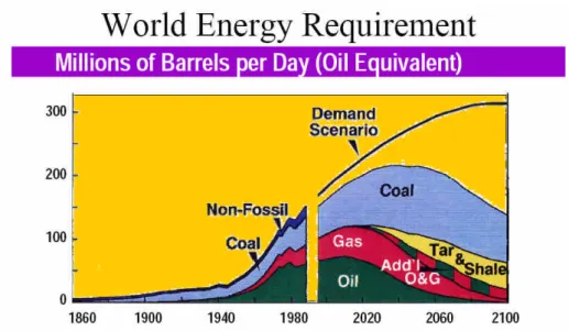
For decreasing the discharge of carbon dioxide, seeking out the replacement is an essential solution unless economizing on energy usage. As revealed by Fig. 1-1-a, the energy requirement is more and more in the future. So the energy resource is replaced by solar energy that is a future tendency.
Fig. 1-1-a The requirement of energy and the tendency of several energy decreasing
Therearealotofuniquepropertiesofsolarenergy such as‘universality’meansthatit exists in everywhere; ‘clean energy’means it does not produce pollution; ‘no time-limit usage’means that the sun has existed for 4.5 billion years, and it will exist about ten billion years. Furthermore, the solar energy is a powerful energy, which provides for usage amount is almost thirty thousand times larger than amount of consumption in the world [1]. As can be seen, how to use the solar energy is the most important topic at present.
1.1.2 Development of solar cells
Recently the solar cell has become an important research subject. The solar cells could be classified as several types of silicon solar cells, inorganic compound solar cells, and organic solar cells according to the materials.
The first inorganic solar cell with power conversion efficiency (PCE) is 6% that was fabricated using silicon by Bell Laboratory in 1945 year [2]. After so many years, the PCE of single crystal silicon solar cell has achieved 24.7% in the academia today [3]. At present,
the silicon solar cells could be separated three types that are single crystal solar cells, polysilicon solar cells, and amorphous silicon solar cells. The single crystal and polysilicon solar cells have the similar fabrication, and the amorphous silicon solar cell is different from them. The amorphous silicon solar cell is a thin film solar cell with the advantages of large area and the low cost that was brought up by D. E. Carlson et al. in 1976 year [4]. The academia could achieve the PCE to 14.5% nowadays [5]. And the thin film solar cell was fabricated by compound material such as CdTe, CuInSe2 (CIS), and Cu(In,Ga)(S,Se)2 with
the PCE 19.2% recently [6].
The single crystal solar cell and the polysilicon solar cell are popular in the market. The single crystal solar cell is almost used in power-station, lighting, and so on. And the polysilicon solar cell is used in low power application because of it is easy to fabricate and the low cost. Besides, the amorphous silicon solar cell has the many electronic products generally since it is the lowest cost in fabrication.
The solar cell properties have stably grown up in the past years. The cost of fabrication is low day by day through development continuously. However, the usage of solar energy is under 0.1% of all the resource consumption so far. It is to know that the high cost of the inorganic solar cell even the technology is mature. Therefore, to develop the fresh type of solar cell is a key point in the future.
Fig. 1-1-b The development of power conversion rate for several solar cell types [7]
1.1.3 Development of polymer solar cells
The organic solar cell was paid attention to heavily research in recent ten years, the device structure advances from single layer to bilayer hetero-junction structure, bulk hetero-junction, and ordered bulk hetero-junction, shown in Fig. 1-1-c. The development tends to increase the transmission path and transmission rate of carriers.
The structure of bilayer hetero-junction is used the energy band gap offset of two component materials to induce the exciton separation, that effectively solves the problem of electron and hole could not separate by thermal energy for single layer structure in the room temperature. Finally separated carriers are collected by electrodes respectively. But the power conversion rate is not high enough because of the carrier separation region is too less (just only in the interface) to achieve high efficiency. The bulk hetero-junction structure increases the efficiency due to the improvement of separation region. After separation, some of the carriers would drift to the dead end and are unable collected by electrodes. For this reason, the next development structure is ordered bulk hetero-junction, that successful solves the problem.
The suitable idea is that integrated hetero-junction and bulk hetero-junction structures of bilayer to become an ordered bulk hetero-junction structure, as revealed by Fig. 1-1-c (d). That structure retains advantages not only the large separation area of bulk hetero-junction, but also the direct transmission path for carriers of bilayer hetero-junction structure. Hence, the ordered bulk hetero-junction is the most effective structure to increase the carrier transmission rate.
So far the organic solar cell could be discriminated from the types of material for small molecular solar cells, polymer solar cells, and dye-sensitized solar cells (DSC).
The small molecular solar cell with 1% was brought up by C. W. Tang in 1986 [9], that was fabricated with copper phthalocyanine (CuPc) and perylenetetra carboxylic-acid debenzimidazole (PV) materials by thermal evaporation. The device structure is to use the bilayer hetero-junction structure to increase the carrier separation rate.
ink-jet printing, blade coating, and so on. The polymer solar cell was developed in 1994 year, which was made by blending polymers and C60 as the active layer [10]. There was a
key idea of the bulk hetero-junction structure that enable expanded the separation region of carriers to everywhere in organic layer, as shown in Fig. 1-1-d. An important opinion about the structure of organic layer influences the development of polymer solar cells subsequently.
Fig. 1-1-d Bulk hetero-junction structure [11]
The first polymer/polymer hetero-junction solar cell with PCE 1% under monochromatic luminescence was presented by Yu et al [12] and Halls et al [13] in 1995 year. The materials were polymer compound of CN-PPV (acceptor) and MEH-PPV (donor). So far the polymer solar cell is used with blending system of P3HT and PCBM with the highest PCE to 6% [14].
Fig. 1-1-e The table of development for polymer solar cells [15]
The DSC with PCE 7.1% was presented by M. Grätzel et al in 1991 year [20]. The DSC is the hybrid solar cell, that fabrication is coating the sensitizer on porous TiO2
and using the electrolyte as medium of hole transmission, as Fig. 1-1-f. The other name of DSC is‘Grätzelcell’or‘photo-electro-chemicalcell’(PEC cell).According to the report [21], the DSC with PCE achieved 12% from Konarka Flexible Plastic DSC Laboratory in 2005 year. The Konarka Company expects that will expand the products scope to enter the electronic market like PDA.
Fig. 1-1-f The working principle of DSC [19]
1.2 Motivation of research
1.2.1 Opportunity for polymer solar cells
There is a very low ratio of the solar energy usage that compares with the petrifaction energy. The main cause of the inorganic solar cell products is the highly expense in the market due to the fact that the usage is not popular today. Consequently, the organic solar cell is paid more and more attention recently because of the remarkably cheaper coating process than inorganic products even if the stability and the efficiency are not as better as inorganic solar cell.
In the many types of solar cell research, the development of DSC is mature than others since it is conformed the properties of the cheap price, the high efficiency, and the reliability has achieved to several thousand hours. But there is a difficult problem for the device packaging with the electrolyte inside although it is a lot of advantageous positions. The safety and convenience of DSC products are influenced by such serious problem. The
other two types of small molecular solar cell and polymer solar cell are tend to stable development since the advantages of the low cost and the easy processes of fabrication. However the fabrication of small molecular solar cell needs the expensive evaporator equipment and the complex process than polymer solar cell. Furthermore, the small molecular solar cell is not easy to scale up to large sizes.
In terms of the many reasons, recently conjugate polymer solar cells have attracted great interests due to their unique properties such as easy solution process for large-area, light weight, and mechanical flexibility. The polymer bulk hetero-junction cells have interpenetrating networks of electron donors and acceptors, resulting in an efficient exciton dissociation and high photo-currents with PCE about 5% [16] [22]. Although the efficiency is not as high as that of inorganic solar cells, the potential of low-cost and roll-to-roll process on flexible substrates makes the polymer solar cells attractive as the solution to the serious energy challenges.
1.2.2 Advantage of blade coating application in polymer solar cells
To date the most of efficient polymer solar cells are made by spin coating, which causes serious material waste and raises the cost dramatically. In addition, the spin coating process is not easy to scale up to very large sizes up to meters and is incompatible with the roll-to-roll process for high throughput production. Furthermore one major problem of the spin coated polymer solar cell is that a very toxic high boiling point organic solvent like dichlorobenzene (180.5 ℃) or chlorobenzene (131 ℃) is necessary for high efficiency. The high boiling point allows a slow drying process where the donor and acceptor molecules self-assemble into an interpenetrating network [16]. The high toxicity of dichlorobenzene and chlorobenzene makes the mass production environmentally unfriendly, and the slow drying process delays the production throughput.
Although there have been researches on fabrication processes, including ink-jet printing [23], screen printing [24], spray coating [25], and blade coating [28], the development of alternative solution coating methods compatible with the low-cost and environmentally friendly mass production remains a crucial problem [27]. Since there is no necessary for organic layers to be structured by printing in organic solar cells, blade coating for large area fabrication has been proved to be the better way [28]. The film thickness by blade coating can be reduced to nanometer scale by carefully controlling the fabrication parameters such as the solution concentration, the blade gap, and the blade coating speed.
We verified the feasibility of blade coating for high efficiency polymer light-emitting diodes [29]. Unlike spin coating, the area can be easily scaled up and the material usage is
almost 100% in blade coating. In this work, blade coating is applied to
poly(3-hexylthiophene) (P3HT) and (6,6)-phenyl-C61-butyric acid methyl ester (PCBM) blend in the toluene solution which has a lower boiling point (110 ℃) and is less toxic. High efficiency is achieved from toluene solution without the slow solvent evaporation process.
1.3 Thesis frameworks for part 1
Chapter 1 IntroductionIntroduced the background, motivation, and purposes of research
Chapter 2 Theory
Introduced the fundamental principles
Chapter 3 Method
Introduced the experimental processes and materials
Chapter 4 Result
Discussed the experimental results
Chapter 5 Conclusion
Summary the important results
Y. H. Chang, S. R. Tseng, C. Y. Chen, H. F. Meng, E. C. Chen, S. F. Horng, C. S. Hsu,’Polymer solar cell by blade coating’, Organic Electronics (2009) in press.
Chapter 2 Theory
2.1 Fundamental principles of solar cells
2.1.1 Equivalent circuit
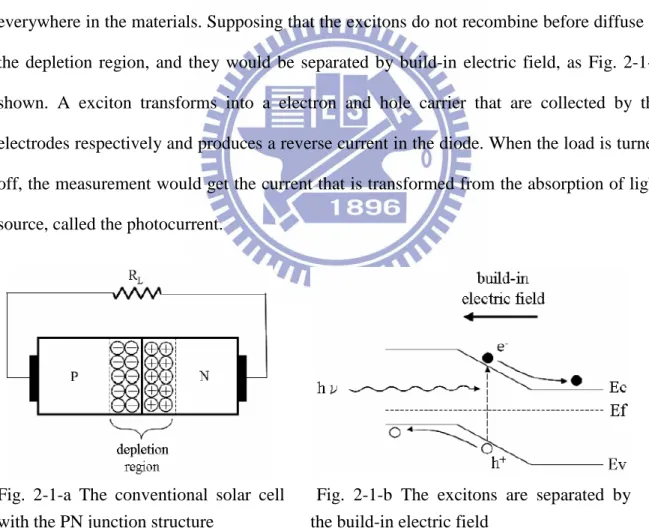
For Fig. 2-1-a, the conventional solar cell is designed as the PN junction structure. There is a single energy band gap Egbetween materials, and the PN junction connects with
a load. When the solar cell absorbs the light with incident energy larger enough than the band gap, the excitons (electron-hole pairs, EHP) would be induced and diffuse to everywhere in the materials. Supposing that the excitons do not recombine before diffuse to the depletion region, and they would be separated by build-in electric field, as Fig. 2-1-b shown. A exciton transforms into a electron and hole carrier that are collected by the electrodes respectively and produces a reverse current in the diode. When the load is turned off, the measurement would get the current that is transformed from the absorption of light source, called the photocurrent.
Fig. 2-1-a The conventional solar cell with the PN junction structure
Fig. 2-1-b The excitons are separated by the build-in electric field
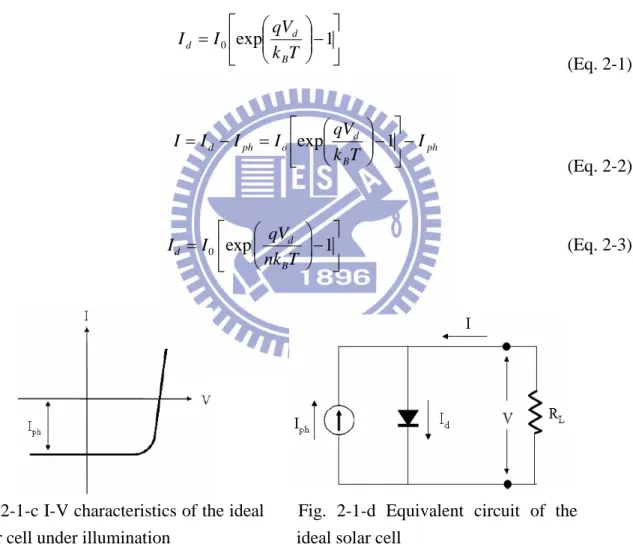
The ideal equation of diode as Eq. 2-1, indicates that the current-voltage characteristics (I-V characteristics). The ideal I-V is called dark current that shows the commutation property of current. It is induced a stable photocurrent under the steady illuminant.
According to the superposition principle for I-V characteristic and the stable photocurrent that obtains the I-V characteristics curve (as Fig. 2-1-c) and the I-V equation (as Eq. 2-2) under a stable power of light source. And the equivalent circuit of the ideal solar cell is shown in Fig. 2-1-d. A diode symbol represents the PN junction and Iph represents the
photocurrent that under the stable power of illumination. However, there are realistic effect of the high-level injection in the PN junction and the recombination of net carrier. For the reasons, it is must added theidealfactor‘n’to correctas Eq. 2-3.
0 exp 1 T k qV I I B d d (Eq. 2-1) ph B d o ph d I T k qV I I I I exp 1 (Eq. 2-2) 0 exp 1 d d B qV I I nk T (Eq. 2-3)
Fig. 2-1-c I-V characteristics of the ideal solar cell under illumination
Fig. 2-1-d Equivalent circuit of the ideal solar cell
In fact, there are problems about series resistance Rs and the leakage current so the
equivalent circuit must correct again. The Rs can be attributed to the semiconductor bulk
and ohmic contact for the electrode in the solar cell device. Fig. 2-1-e shows an equivalent circuit of the realistic solar cell, Rsindicates the total series resistance from the generation
factor of materials or experiments, and the Rshindicates the shunt resistance. The Rsand Rsh
are shown as Eq. 2-4 and Eq. 2-5 under illumination [30].
Fig. 2-1-e Equivalent circuit for a real solar cell
out out V s dI dV R out lim (Eq. 2-4)
out
s sh out out sh V R R dI dV R 0 , (Eq. 2-5)
ph sh s B s I R IR V T nk IR V q I I 0 exp 1 (Eq. 2-6)Therefore, the I-V equation of the realistic solar cell shows in equation 2-6. Fig. 2-1-f shows the I-V characteristics of real solar cell, which is considered with the diode properties and the effect for Rsand Rsh. The curve indicates the current is not a stable value under the
reverse bias, and the current would exchange with the voltage under the positive bias. At the same time, the I-V characteristic is not a vertically rising line. All of the appearance for I-V characteristics is produced from the Rs and Rsh. The I-V characteristics respond to the
Fig. 2-1-f I-V characteristics of the ideal solar cells and the real solar cells under illumination
ph B s I T nk IR V q I I 0 exp 1 (Eq. 2-7) ph sh B I R V T nk qV I I 0 exp 1 (Eq. 2-8)I-V characteristic equation (Eq. 2-6) of equivalent circuit for solar cells could be simplified to Eq. 2-7 and Eq. 2-8. The I-V characteristic is influenced by Rshwhen the diode
current Id is much larger than the leakage current Vd/ Rsh, then Rsh became a slight factor
simultaneously. Therefore the Eq. 2-6 could be replaced by Eq. 2-7.When the Idis equal to
the Vd/ Rsh, then Rshis a notable factor under the weak illuminant, so the Eq. 2-6 could be
correct to Eq. 2-8.
The Fig. 2-1-g shows the I-V characteristics of the silicon solar cell with a stable photocurrent density under a stable illuminant. In Fig. 2-1-g (a) the Rs not only influences
the fill factor (FF, introduction in 2-1-2 section) but also exchanges a tendency toward short-circuit current (Isc, introduction in 2-1-2 section) becomes smaller and Rs becomes
slightly decreased with the Rshis dropped off.
Fig. 2-1-g The I-V characteristics of a solar cell of (a) different Rsand (b) different Rsh[31]
2.1.2 Basic parameters
The fundamental parameters of solar cell are the short-circuit current (Isc), the
open-circuit voltage (Voc), the fill factor (FF), the power conversion efficiency (PCE), and
the external quantum efficiency (EQE). Fig. 2-2-a shows relation between the I-V characteristic and the parameter definition.
Fig. 2-2-a The relation between the I-V characteristics and the parameter definition of a solar cell [32]
A. Short-circuit current (Isc)
From the I-V characteristics, the solar cell could be measured with I-V relation by changing the load under a stable illumination. When the load is equal to zero, the current is called short-circuit current, Isc, as shown in Fig. 2-2-a point (a). Without consideration of
leakage current, the Iscindicates the photocurrent as Isc= Iph.
B. Open-circuit voltage (Voc)
When the load tends to be unlimited and the current is equal to zero, the voltage is called the open-circuit voltage, Voc, as the point (b) in Fig. 2-2-a. The working region of the
solar cell is in the fourth quadrant, which is the load exchange from zero to large limit.
C. Fill factor (FF)
In the working region of a solar cell, there is a maximum output power (Pmax) under a
current and voltage that are indicated as Impp and Vmpp separately shown in Fig. 2-2-a. The
Pmaxis equal to multiply the two values as Eq. 2-9. FF is a ratio between Pmaxand Isc×Vocas
Eq. 2-10. FF indicates the turn-on properties of the I-V characteristics in the fourth quadrant and can help us to know the Rsand Rshhow to influence on solar cell.
max max max I V P (Eq. 2-9) oc sc oc sc I V V I V I P
FF max max max
(Eq. 2-10)
D. Power conversion efficiency (PCE)
The power conversion efficiency is a ratio with the maximum output power and the power of incident illuminate. The Pmaxcould be obtained from the Isc, Voc, and FF as shown
in Eq. 2-11. in sc oc in ax m P I V FF P P (Eq. 2-11)
E. External quantum efficiency (EQE)
The external quantum efficiency (EQE) indicates conversion efficiency between the incident photon numbers and the induced photocurrents. It is a ratio with the output electron numbers and the incident photon numbers. As shown in Eq. 2-12, the external quantum efficiency is relative to the wavelength of incident light, the power, and the Isc, and has no
relationship with the Voc and FF. The value of the Iscis relative to the EQE. The EQE could
) ( 1240 nm P I n InputPhoto tron OutputElec EQE in sc (Eq. 2-12) CC CS ED A EQE
(Eq. 2-13)Fig. 2-2-b shows the EQE that could be separated by the four parameters with ηA, ηED,
ηCS, and ηCCthrough the process from the photon absorption to the carrier collection. The
sequence of the four factors is expressed the conversion process from photons to electrons. The main factors to affect the EQE are ηCSand ηCC.
Symbol Appellation Effect
ηA Absorption efficiency
The efficiency of absorbed illumination for devices.
ηED Exciton diffusion efficiency
The efficiency of the exciton diffusion to the material interface.
ηCS Carrier separation efficiency
The efficiency of the exciton separation in the material interface.
ηCC Carrier collection efficiency
The efficiency of the carrier transmission and collection by the electrodes.
Fig. 2-2-b The energy band of the material interface and the electrode in short-circuit condition
2.2 Characteristics of conjugate polymer materials
2.2.1 Development
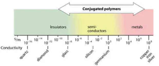
The polymer semiconductor was jointly discovered by the A. G. MacDiarmid, A. J. Heeger, and Hideki Shirakawa since 1977 year. They used the polyacetylene with doping the iodine. The degree of electric conduction was increased over one hundred million times [33]. After about thirty years, there are a lot of the important research results for conjugate polymer. The three of the scientists have obtained the chemical Nobel Prize in 2000 year. The conjugate polymers are many developments in the various photovoltaic regions, and will prosperous expand in the future.
2.2.2 Photovoltaic property
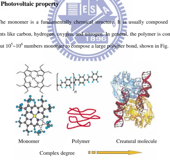
The monomer is a fundamentally chemical structure. It is usually composed by the elements like carbon, hydrogen, oxygen, and nitrogen. In general, the polymer is composed of about 105~106numbers monomer to compose a large polymer bond, shown in Fig. 2-2-c.
Fig. 2-2-c The complex degree of the organic materials
Monomer Polymer Creatural molecule
The carbon element on the back-bond for conjugate polymer has the unsaturated bond so that composes an alternate bonding with single and double bond. The conjugate single-bond and double-bond is called the conjugate bonding. The simplest conjugate polymer is polyacetylene as Fig. 2-2-d.
Fig. 2-2-d Polymer molecular structure of polyacetylene
From the electronic orbital theory, there is an electron on the sp2 orbit among the carbon atom that combines with the hydrogen atom, and the other two sp2 orbits combine with another sp2 orbit for the nearest carbon atoms that become the single σ-bond. Nevertheless, the σ-bond is not beneficial for electronic transmission because that has the properties with the large band gap, the narrow energy width, and the small molecular orbit. In addition, the vertical orbit of the sp2 plane overlaps with the other orbit for the nearest carbon atoms, attributed to adelocalized π-band. That enables electrons to move on the polymer chains that induces the electronic conduction. Therefore, the conjugate polymer is called the conducting polymer. The special property of the conjugate polymer is the electronic conduction that could be controlled by doping to a conductor or an insulator as Fig. 2-2-e.
Chapter 3 Method
3.1 Experimental system
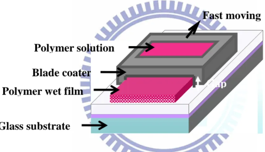
3.1.1 Working principle of blade coating
Fig. 3-1-a shows the schematic working principle of blade coating. The thickness of the wet polymer film is defined by the gap. The polymer dry film thickness is tuned by the polymer concentration in solution and the gap of the blade coater. The polymer wet film is deposited by dragging the blade coater at a certain speed about 15 cm/s.
Fig. 3-1-a Schematic working principle of blade coating
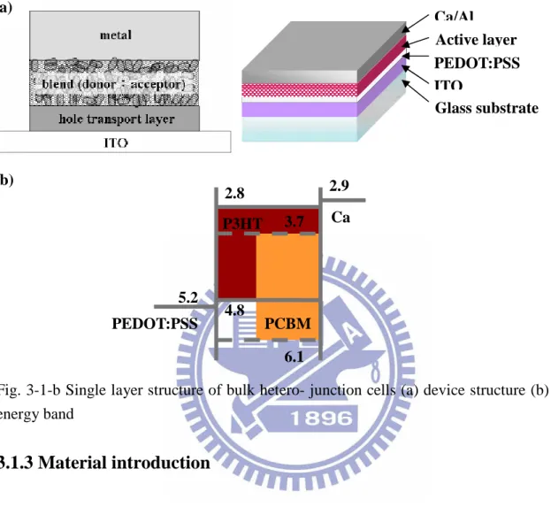
3.1.2 Device structures
The development of the organic solar cells is to develop multilayer device structure and the bulk hetero-junction devices. Considering all of the development processes, the main idea is to increase the separation region for excitons. In this study, we used the bulk hetero-junction structure with single layer. The bulk hetero-junction device is made by the P3HT donor and PCBM acceptor blending. The device structure is designed for ITO/PEDOT:PSS/P3HT:PCBM/Ca/Al shown in Fig. 3-1-b (a). ITO is the anode and PEDOT:PSS (Baytron PVP AI 4083) is the hole transport layer. The active layer is used the
Glass substrate Polymer wet film
Blade coater
Gap
Fast moving Polymer solution
P3HT and PCBM blending in organic solvent, and the cathode Ca/Al is used. The energy band for the structure is shown in Fig. 3-1-b (b).
Fig. 3-1-b Single layer structure of bulk hetero- junction cells (a) device structure (b) energy band
3.1.3 Material introduction
A. Hole transport layer
For Fig. 3-1-c, the hole transport layer is poly-(3,4-ethylenedioxythiophene): poly-(styrenesulfonate) (PEDOT:PSS) with LUMO of 3.6 eV and HOMO of 5.2 eV. The PEDOT is an aqueous solution of polymer. It is not only for the hole transport but also for flattening the ITO substrate. In addition, the PEDOT:PSS layer conforms with the advantage of the light transmission. According to the different ratio between PEDOT and PSS has the different types and resistance. As the type of AI4083 is 1:6 ratio for PEDOT:PSS and the volume resistivity is about 500-5000 ohm-cm.
PEDOT:PSS Glass substrate ITO Active layer Ca/Al P3HT 3.7 6.1 4.8 2.8 Ca PEDOT:PSS 5.2 2.9 PCBM (b) (a)
Fig. 3-1-c Molecular structures of PEDOT and PSS
B. Active layer
The active layer is used the P3HT and PCBM blending in organic solvent. The poly(3-hexylthiophene) (P3HT) with LUMO of 2.8 eV and LUMO of 4.8 eV is a common donor of polymer material that with the absorption wavelength among 500nm~600nm. In general, the electron mobility (μe= 10-4~10-9 cm2/V-s) is lower than the hole mobility (μh=
10-1~10-7 cm2/V-s) for polymers. Therefore the better donor material is chosen with the higher hole mobility. P3HT is a better hole mobility among the conjugate polymer. It had
been measured the hole mobility about 10-1 cm2/V-s [33]. Besides, the
(6,6)-phenyl-C61-butyric acid methyl ester (PCBM) with LUMO of 3.8 eV and HOMO of 6.2 eV is a common acceptor of small molecular material. It is a derivative for C60that has
the higher electron transport ability and the absorption wavelength is about 350nm. But the PCBM could not be easily dissolved in organic solvents by itself that needs some other polymer material as guest to increase solubility.
Fig. 3-1-d The monomer structure of P3HT
Fig. 3-1-e The molecule structure of PCBM
3.2 Experimental process and measurement
3.2.1 Deposition of the hole transport layer
The patterning ITO coated glass substrates were cleaned by ultrasonic treatment with organic solvent, detersive and deionizer water successively. After removing the smirch on the substrate, the cleaned substrates were baked on hot plate with 100 ℃ for several minute. Then ITO substrates are treated by UVO3 with 20 minutes for the formation a
hydrophilic surface. PEDOT:PSS (Baytron PVP AI 4083) film with the thickness about 40 nm as hole transport layer was spin coated in air and then baked at 200 ℃ for 15 minutes in nitrogenous glove box.
3.2.2 Deposition of the active layer
The blend of P3HT:PCBM with 1:1 ratio formulated 17 mg/ml respectively dissolved in toluene, chlorobenzene (CB), and dichlorobenzene (DCB). The solutions were heated at 60 ℃ for 12 hours at least. We first focus on solar cells with P3HT:PCBM blend dissolved in toluene. Device performances are compared for different coating methods including spin coating, blade coating, blade coating on a hot plate, as well as blade and spin coating. For the blade and spin coating the polymer wet film is deposited by blade coating which is followed by spinning until the dry film is formed.
Seven series of devices with six devices in each are made to study the different coating processes with different solvents statistically. Among them, five series are made with toluene solution to compare the coating processes, including spin coating (series A), blade coating (series B), blade coating on a hot plate at 60℃ (series C), as well as blade and spin coating (series D). In addition, the devices with the PEDOT:PSS layer by blade coating at 100℃ and P3HT:PCBM by blade and spin coating from toluene solution is made to study
the feasibility of bladed PEDOT:PSS layer (series G). The other two series made from two conventional high boiling point solvents, chlorobenzene (series E) and dichlorobenzene (series F), are compared with those from toluene by blade and spin coating. After coating all the P3HT:PCBM layers are annealed at 140℃ for 20 minutes in nitrogen.
The Ca(35nm)/Al(100nm) cathode was deposited by thermal evaporation. The active area of the device was 0.04 cm2. All the devices were packaged in the glove box and measured in the ambient environment.
3.3 Measurement
3.3.1 Photovoltaic property
The PCE is measured by the solar simulator (PEC-L11, Peccell Technologies) under AM1.5G irradiation.
3.3.2 External quantum efficiency
The incident photon-to-electron conversion efficiency (IPCE) is measured by the spectral response measurement system (SR300, Optosolar GMBH).
3.3.3 Morphology
The morphology of P3HT:PCBM is monitored by atomic force microscope (AFM, Dimension 3100, Digital Instruments).
Chapter 4 Result and discussion
4.1 Device performance of bulk hetero-junction cells
Fig. 4-1-a shows the statistical results of the seven series of devices. Among the series based on toluene solution (series A, B, C, D, and G), the series of devices by blade coating have the higher efficiencies except the series with bladed the PEDOT:PSS layer. Because the Vocare about the same, the high performances of series B, C, and D result from the high
short circuit current density Jsc and fill factor. Among the series by blade and spin coating
(series D, E, and F), the series of devices from toluene solution and dichlorobenzene have the higher performances. While the Jsc of series E and series F are about the same, the high
performance of series F results from the relatively high fill factor. For further discussion, the best devices in each series are chosen to show the advanced device properties.
Fig. 4-1-a Statistical results of the seven series of devices, (a) the PCE, (b) the Jsc, (c) the
Voc, and (d) the fill factor. The horizontal lines in the box denote the 25th, 50th, and 75th
percentile values. The error bars denote the 5th and 95 percentile values. The open square inside the box denotes the mean value.
Fig. 4-1-b (a) shows the current density-voltage (J-V) curves of five devices in toluene solution made by different active layer coating processes. The short circuit currents Jscmade
by blade coating (device B, C and D) are larger than that of the device made by conventional spin coating (device A). Using blade coating the Jsc increases from 9.3
mA/cm2 with spin coating to 11.5 mA/cm2. The fill factor rises from 47% to 55% and the Voc remains the same. The efficiency, which is proportional to Jsc, Voc, and fill factor as a
whole, is improved from 2.6% (device A) by spin coating to 3.8% (device C) by blade coating on a hot plate.
(c)
(d)
(a)
(b)
A B C D E F G 2.0 2.5 3.0 3.5 4.0 P o w e r c o n v e rs io n e ff ic ie n c y (% ) Series A B C D E F G 7 8 9 10 11 12 S h o rt -c ir c u it c u rr e n t d e n s it y ( m A /c m 2 ) Series A B C D E F G 0.57 0.58 0.59 0.60 O p e n -c ir c u it v o lt a g e (V ) Series A B C D E F G 40 45 50 55 60 65 70 F il l fa c to r (% ) SeriesFig. 4-1-b Current density-voltage (J-V) relations of the devices. (a) Devices made by spin coating (device A, solid square), blade coating (device B, empty square), blade coating at 60 ℃
(device C, solid circle), and blade and spin coating (device D, empty circle) in toluene solution, blade and spin coating with bladed PEDOT:PSS (device G, solid star) (b) Devices made by blade and spin coating in toluene solution (device D, empty circle), chlorobenzene solution (device E, solid triangle), and dichlorobenzene solution (device F, empty triangle)
0.0
0.2
0.4
0.6
-12
-10
-8
-6
-4
-2
0
C
u
rr
e
n
t
d
e
n
s
it
y
(
m
A
/c
m
2
)
Voltage (V)
Device D (Toluene) Device E (Chlorobenzene) Device F (Dichlorobenzene)Blade and spin coating
0.0
0.2
0.4
0.6
-12
-10
-8
-6
-4
-2
0
C
u
rr
e
n
t
d
e
n
s
it
y
(
m
A
/c
m
2
)
Voltage (V)
Device A (Spin) Device B (Blade) Device C(Blade, 60OC)Device D (Blade and spin) Device G(Blade and spin, Bladed PEDOT) Toluene solution
(a)
It is believed that in order to get a high efficiency in bulk hetero-junction polymer solar cell the microscopic morphology of the active layer needs to be well controlled to achieve an ordered structure by certain annealing processes such as slow solvent evaporation1 and postproduction heat treatment [22]. Such annealing promotes molecular self-organization and makes the polymer chains more ordered in its domains. In spin coating for low boiling point solvents such as toluene (110 ℃), high volatility leads to the fast drying of the active layer and may limit the self-assembly as well as the PCE. However, the polymer films made by blade coating could be more ordered than those by spin coating due to the fact that the polymer chains are relatively free to move in the absence of centrifugal force. Therefore even without the slow drying process the donors and acceptors quickly self-assemble into the desired ordered and interpenetrating morphology during the blade coating process. We speculate that the quick assembly occurs at the beginning of the blade coating because the device made by blade and spin coating (device D) shows high efficiency as well. Interestingly, device B, C, and D have different film thickness but similar performances. High efficiency is maintained for device B with 412 nm thickness probably because pure blade coating with neither heating nor spinning give the highest freedom to chain motions and the most ordered morphology. In short, the blade coating method allows ordered polymer morphology in a fast drying solution like toluene. In addition, the result of the device with the bladed PEDOT:PSS and blade and spin coated P3HT:PCBM layer is also shown in Fig. 4-1-b (a). The efficiency of device G is 2.5% with Jscof 8.35 mA/cm2, Vocof
0.59 V, and fill factor of 52%. The relative low performance of device G results from the thick PEDOT:PSS film (120 nm), which causes high series resistance. It is difficult for us to reduce the PEDOT:PSS film thickness now because we use the PEDOT:PSS solution from H. C. Stark without any further dilution. The concentration needs to be lowered without sacrificing the conductivity to get the normal film thickness (40 nm). More experiments need to be done to optimize the PEDOT:PSS layers by blade coating. Nevertheless, such
device shows the feasibility of all blade coated devices with very low cost and high throughput in mass production.
Now we turn to different solvent systems. Two devices are made by conventional high boiling points solvents chlorobenzene (device E) and dichlorobenzene (device F). Fig. 4-1-b (b) shows the results of the devices by the fast-drying blade and spin process with different solvents. There is no slow solvent evaporation in the fabrication process. The power conversion efficiencies are 2.5% in the device from chlorobenzene solution (device E) and 3.5% in that from dichlorobenzene solution (device F). The Jsc are both about 8.8 mA/cm2,
which is significantly smaller than Jsc of 11.4 mA/cm2 in device D from toluene.
Interestingly high boiling point solvents give higher Jsc for spin coating but smaller Jsc for
blade coating. There are probably more P3HT/PCBM interfaces in toluene solution than those in chlorobenzene and dichlorobenzene solutions, resulting in more efficient exciton dissociation. It is remarkable that the fill factor of dichlorobenzene solution is 66 %, much higher than 55 % for toluene and 49 % for chlorobenzene. Dichlorobenzene has the highest boiling point among the three solvents. The highest fill factor in dichlorobenzene solution may result from the highest carrier mobility due to the enhanced self-assembly of P3HT taking place during the relatively slow drying in spinning. The device performances are summarized in Table 1.
Table 4-1 Performance of bulk hetero-junction solar cells in this work. Label Jsc (mA/cm2) Voc (V ) Fill factor (%) PCE (%) Thickness (nm) A. (Toluene)Spin 9.25 0.59 47 2.6 223 B. (Toluene)Blade 11.07 0.59 53 3.5 412 C. (Toluene)Blade at 60℃ 11.49 0.59 55 3.8 304 D. (Toluene)Blade and spin 11.36 0.58 55 3.7 245 E. (Chlorobenzene)Blade and spin 8.87 0.57 49 2.5 345 F. (Dichlorobenzene)Blade and spin 8.79 0.60 66 3.5 242 G. (Toluene)Blade and spin
with bladed PEDOT:PSS (120 nm) 8.35 0.59 52 2.5 245
The AFM images of the devices are shown in Fig. 4-1-c. The root-mean-square (RMS) roughness are 2.3 nm for device A, 15.1 nm for device B, 4.9 nm for device C, 2.8 nm for device D, 1.9 nm for device E, and 5.8 nm for device F. The different root-mean-square values are attributed to the different fabrication processes with different solvents. We think that the devices with high efficiency (device B, C, D, and F) have stronger self-organization than those with low efficiency (device A and E). Higher surface roughness corresponds to higher degree of self-organization [34]. However, there is no clear evidence for the correlation between self-organization and device efficiency. Nevertheless, we speculate that device B by blade coating shows clear self-organization, implying ordered structures within each component. Therefore, the carrier mobility is high and the power conversion efficiency is high as well even with a thick film of 412 nm. The clear self-organizations in device C and device F also could be seen due to their relative high roughness. Interestingly, the roughness of device D by blade and spin coating is just slightly higher than that of device A only by spin coating, but the efficiency of device D is still much higher. This may be due to the ordered structure occurred at the beginning of blade coating, combined with thicker film thickness by blade coating. As for the low efficiency devices such as device A and device E, the films are relatively smooth. The images show that the self-organization could be
achieved within the short drying time by blade coating.
Fig. 4-1-c AFM images of the devices in this work. P3HT:PCBM thin film made by (a)spin coating, (b)blade coating, (c)blade coating at 600C, (d)blade and spin coating, (e) blade and spin
coating in chlorobenzene solution, (f) blade and spin coating in dichlorobenzene solution. The P3HT:PCBM films in (a) to (d) are made in toluene solution.
Fig. 4-1-d (a) shows the absorption spectra of the P3HT and PCBM blend films deposited by different methods and solutions. The IPCE for all devices are shown in Fig. 4-1-d (b). Despite of the different morphologies there is no significant variations among the absorption spectra. So the differences in the device performances must come from the exciton dissociation and carrier transport processes. The IPCE values appear similar in all the devices except that of device G and show slightly difference at about 600 nm. However, the Jscvalues show much difference among the devices. In principle the measured Jscshould
Blade + spin (Chlorobenzene) Blade + spin (Dichlorobenzene)
Rms:5.8 nm
15.0 nm 0.0 nm 30.0Rms:1.9 nm
5.0 nm 0.0 nm 10.0Rms:2.8 nm
5.0 nm 0.0 nm 10.0Rms:4.9 nm
10.0 nm 0.0 nm 20.0Rms:15.1 nm
25.0 nm 0.0 nm 50.0Rms:2.3 nm
5.0 nm 0.0 nm 10.0 Spin (Toluene) Blade (Toluene) Blade, 600C (Toluene) Blade + spin (Toluene) 0 5 μ mbe proportional to the product of the IPCE and the illuminating spectrum, integrated over all wavelengths. We may attribute the inconsistency between IPCE and Jsc values to the
different spectral-mismatch factors of the different light sources [26].
Fig. 4-1-d (a) The absorption spectra of devices. (b) The incident photon to current efficiency (IPCE) in this work
400
500
600
700
0.0
0.2
0.4
0.6
0.8
1.0
Device ADevice B Device C Device D Device E Device FA
b
s
o
rp
ti
o
n
(a
.u
.)
Wavelength (nm)
(a)
400
500
600
700
0
10
20
30
40
50
60
70
IP
C
E
(%
)
Wavelength (nm)
Device A Device B Device C Device D Device E Device F Device G 400 500 600 50 60 70 IP C E (% ) Wavelength (nm)(b)
4.2 Roughness of net P3HT and PCBM film
Fig. 4-2-a and Fig. 4-2-b show the morphology of thin film for net P3HT and pure PCBM with the same experiment conditions between Fig. 4-1-c like the fabrication processes and the solvents for each components. It is easy to discover the difference between the properties of grown net P3HT and PCBM thin film. All of the net P3HT films have the root-mean-square (RMS) roughness with about 15±3 nm that tends to form the aggregation between P3HT polymers. However, there seems not be clear division among the different fabrication processes and different organic solvents. We turn to observe that the roughness of PCBM, it is evident that the film property is greatly different between net P3HT films. The PCBM films have the tendency to form the crystals because the roughness becomes much higher. A lower RMS case (Fig. 4-2-b, sample F) among the net PCBM films that may due to the experimental variation such as the film thickness or the man-made effect during blade coating process.
The films of P3HT and PCBM blending have the lowest roughness among three types that can be attributed to mutually restrain the effect on aggregation for P3HT and the crystal for PCBM.
Fig. 4-2-a AFM images of net P3HT thin film made by (a)spin coating, (b)blade coating, (c)blade coating at 600 C, (d)blade and spin coating, (e) blade and spin coating in
chlorobenzene solution, (f) blade and spin coating in dichlorobenzene solution. The P3HT films in (a) to (d) are made in toluene solution.
Fig. 4-2-b AFM images of the PCBM thin film made by (a)spin coating, (b)blade coating, (c)blade coating at 600 C, (d)blade and spin coating, (e) blade and spin coating in
chlorobenzene solution, (f) blade and spin coating in dichlorobenzene solution. The PCBM films in (a) to (d) are made in toluene solution.
Table 4-2 The roughness of P3HT:PCBM, net P3HT, and net PCBM films
Label RMS (nm)
P3HT:PCBM P3HT PCBM
A. (Toluene)Spin 2.3 14.7 60.3
B. (Toluene)Blade 15.1 18.2 36.31
C. (Toluene)Blade at 60℃ 4.9 12.7 35.3
D. (Toluene)Blade and spin 2.8 18.1 59.1
E. (Chlorobenzene)Blade and spin 1.9 13.9 51.7
Chapter 5 Conclusion
In conclusion we develop the blade coating method to fabricate bulk hetero-junction polymer solar cells with decent power conversion efficiency of 3.8 %. The active layer is deposited from toluene solution, which is less toxic than the chlorobenzene and dichlorobenzene solution optimized for spin coating. In sharp contrast to spin coating there is almost no material waste in blade coating. Moreover, this method can be easily scaled up to large sizes as meters and can be applied in a future roll-to-roll fashion for mass production.
Part 2 Multilayer polymer photo-detectors
Chapter 6 Introduction of polymer
photo-detectors
6.1 Background of research
6.1.1 Introduction of polymer proximity sensors
Proximity sensor is the device which can sense the approaching objects without contact. According to the different materials, it could be classified as the inorganic proximity sensor and the polymer proximity sensor. Today the inorganic proximity sensor has been well developed and applied to the mechanical robot in automatic products. However the fabrication of the inorganic proximity sensor needs the high fabrication temperature, complex processes, the inflexibility property, and the high cost. Besides, there are some problems of inorganic proximity sensor such as the difficulty to scare up to the large-area size with high density sensing array. On the contrary, the polymer proximity sensor has the advantages like the low cost fabrication, easy fabrication processes from solution, large-area with high density array, and the potential of the flexibility. The polymer proximity sensors can be extensive applied in the robot skin that could increase the usage region such as in the safety, nursing, housework, and so on.
Fig. 6-1-a Inorganic proximity sensors
6.1.2 Development of polymer proximity sensors
The proximity sensor is made by a light-emitting diode as light source and a photo-detector as light receiver. In 1963 year, the first organic light-emitting diode (OLED) was made by anthracene crystal as emission layer material; it was a poor device performance [36]. Until 1987 year, Kodak used the Alq3as the emission layer to fabricate a
green light OLED with the low operation voltage (below 10 volts). Until 1990 year, the polymer light-emitting diode (PLED) was developed by Friend Group in England. The PLED was made with poly(p-phenylene vinylene) (PPV) by spin coating [37]. Recently, the PLED is developed with quick speed for the high efficiency and high luminance.
The photo-detector has the same device structure as polymer bulk hetero-junction solar cell in this work. The difference between photo-detector and solar cell is the operating voltage. The photo-detector is operated under reverse biases. The reverse bias is applied to improve the carrier transport ability to increase the carrier collection by electrodes. The relative introduction of the polymer solar cell development is in the section 1-1-3.
Fig. 6-1-b shows the proximity sensor device is composed by a light source PLED and a polymer photo-detector. The working principle of the proximity sensor is that the light is emitted from PLED, reflected by the approaching object surface, and then sensed by the photo-detector. In short, the photo-detectors transform the absorption photons to electrons, and the current change is detected to sense the distance between the objects.
Fig. 6-1-b Schematic the working principle of polymer proximity sensor
The performance of the polymer photo-detector is relative with the current-voltage in the reverse biases shown in Fig. 6-1-c (a), which is different from the solar cell with a small forward bias shown in Fig. 6-1-c (b).
Fig. 6-1-c The current-voltage curves (a) photo-detector device with a reverse bias [38] (b) solar cell device with a positive bias [39]
Object
Polymer photo-detector PLED
6.2 Motivation of research
6.2.1 Problems of polymer photo-detectors
A good polymer proximity sensor should have good performance for the light source and the photo-detector. In this study, we focus on the high sensitivity photo-detector that implies the device with high photocurrent generation and low dark currents. The photocurrent generation is decided by materials, fabrication processes of active layer, and the microscopic morphology between the components. Otherwise the dark current comes from the operation in the reverse bias. Apply a reverse bias in order to increase carrier transport ability of the active layer to increase the efficiency of the carrier collection by electrodes. But that would induce the serious dark carrier injection to form the dark current at the same time. The so-called dark carrier is the electrons injected from the anode and the holes injected from the cathode as well, shown in Fig. 6-2-a. The dark carrier transmissions direct is opposite to the photocurrent, which would reduce the photo-detector sensitivity. In order to improve the sensitivity, the dark current need to be reduces because the measurement current is the total current of photocurrent and dark current.
Fig. 6-2-a The origin of dark current
Donor Acceptor Anode Cathode
e
-h+6.2.2 Multilayer structures
The multilayer structure is designed to solve the problem of high dark current by introducing the carrier blocking layers to avoid dark carrier injections. The blocking layers are designed as electron blocking layer (EBL) and hole blocking layer (HBL). Fig. 6-2-b shows the energy band diagram. The additional EBL between anode and active layer could form a barrier to avoid the electron injection from anode. The other side is HBL between active layer and cathode to avoid the hole injection from cathode.
Fig. 6-2-b Multilayer structure of photo-detector to reduce the dark carrier injection (a) device structure (b) energy band
The multilayer structure is not easy to achieve by solution process because of there is a serious dissolution problem between polymer layers. In general, multilayer devices can be achieved by liquid buffer layer (BL) [40] and polymer transfer printing [41]. Another problem is the small molecule could not be deposited directly by solution processes for one component material generally because small molecules do not have side-chains or main-chains to form a thin film as Fig. 6-2-c
Anode
Electron blocking layer
Active layer Cathode Hole blocking layer
Anode HBL
![Fig. 1-1-b The development of power conversion rate for several solar cell types [7]](https://thumb-ap.123doks.com/thumbv2/9libinfo/8256930.171929/16.892.141.780.109.782/fig-development-power-conversion-rate-solar-cell-types.webp)
![Fig. 1-1-d Bulk hetero-junction structure [11]](https://thumb-ap.123doks.com/thumbv2/9libinfo/8256930.171929/18.892.193.747.364.757/fig-d-bulk-hetero-junction-structure.webp)
![Fig. 2-2-a The relation between the I-V characteristics and the parameter definition of a solar cell [32]](https://thumb-ap.123doks.com/thumbv2/9libinfo/8256930.171929/29.892.255.676.119.448/fig-relation-i-characteristics-parameter-definition-solar-cell.webp)