CHAPTER I
INTRODUCTION
1.1
M
ICRO-E
LECTROM
ECHANICALS
YSTEMSB
ACKGROUNDIt can be said the field of Micro-ElectroMechanical Systems (MEMS) was originated by the paper of Richard P. Feynman in 1959. MEMS generated huge excitement in the mid-1980’s with the demonstration of the first functioning silicon micromotor [1, 2]. The micromotor was constructed by a thin-film deposition process and could be operated by electrostatic actuation as shown in Fig.1.1. This accomplishment led to wide spread speculation about the potential world changing impact of this merging technology.
Figure 1.1 Poly-Si micromotor [2]
Many miniature devices fabricated by the technology, their operation methodologies depend on physical principles converted, electrical signals applied and mechanical structure designed. Merged the principles of actuation and sensing, the microactuators and microsensors are created with functions of motion and
detection. Existing useful devices applied in daily human life includes sensors and actuators suc h as accelerometers [3] (Figure 1.2a), pressure sensors [4], printer head [5] and digital micro-mirror device [6] (Figure 1.2b) fabricated by micromachining and CMOS processes. In the future, MEMS revolutionize nearly every product category by bringing together silicon-based microelectronics with micromachining technology, making possible the realization of complete systems-on-a-chip. MEMS is an enabling technology allowing the development of smart products, augmenting the computational ability of microelectronics with the perception and control capabilities of microsensors and microactuators and expanding the space of possible designs and applications.
(a) Accelerometer [3] (b) Digital Micro-mirror Device [6] Figure 1.2: Commercialized MEMS products
Microelectronic integrated circuits can be thought of as the "brains" of a system and MEMS augments this decision-making capability with "eyes" and "arms", to allow microsystems to sense and control the environment. Sensors gather information from the environment through measuring mechanical, thermal, biological, chemical, optical, and magnetic phenomena. The electronics then process the information derived from the sensors and through decision making
capability direct the actuators to respond by moving, positioning, regulating, pumping, and filtering, thereby controlling the environment for given desired outcome or purpose. These microsystems will require a synergism among many different disciplines and working together to overcome its challenges will ens ure the early utilization of MEMS to benefit mankind and have a profound effect on society. Moreover, MEMS devices are manufactured using batch fabrication techniques similar to those used for integrated circuits, unprecedented levels of functionality, reliability, and sophistication can be placed on a small silicon chip at a relatively low cost.
1.2
O
PTICALC
OMMUNICATIONS
YSTEMSDevelopment of fibers and devices for optical communication began in early 1960s and continues strongly today. But the real change came in the 1980s. During this decade, optical communication in public communication networks developed from the status of a curiosity into being the dominant technology.
The most important development in optical communication since the development of low-loss optical fibers is the erbium-doped fiber amplifier (EDFA) [7]. The EDFA overcame the earlier power-budget limitation of transmission systems and pushed the transmission limitations forward to become dispersion-limited instead. The EDFA broke through as a commercially mature technology in 1994. The first commercial transocean system, which made use of EDFA technology, was installed in 1995 as the Trans-Atlabtic Telephone, TAT-12/13 cable network [8]. It had a bit rate capacity of 5 Gb/s on a single wavelength, and upgraded to 20Gb/s during 1999 with WDM technology. WDM which is the ability to send many independent optical channels on a single fiber is a major step toward fully optical networking. The dense WDM ensure a
throughput of 64 wavelengths per fiber pair, and each wavelength carrying 10 Gb/s the total capacity will amount to 5.12 Tb/s.
In general, there are two basic means of increasing the capacity of fiber communication system, either by time -division multiplexing (TDM) or with WDM technologies. As early as 1994, TDM was the preferred choice. The TDM upgrade the bit rate is so high that dispersion becomes the major problem to be overcome. On the other hand, the commercial breakthrough for the WDM technique came in 1996 due to the development of the EDFA. Thus, the capacity of most advanced WDM systems was attained [9].
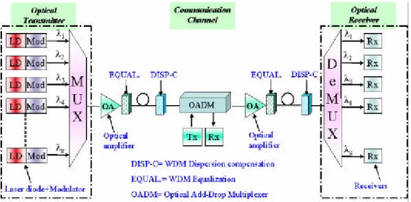
WDM involves a small number of physical-layer functions. These are depicted in Figure 1.3 [10], which shows a WDM schematic for numerous channels occupied its own wavelength. It consists of a transmitter, a communication channel, and a receiver, the three elements common to all communication systems. The WDM system enhances the transmission capacity on a point-to-point basis. The system performs the following main functions:
• Generating the signal— The source, a solid-state laser, must provide stable light within a specific, narrow bandwidth that carries the digital data, modulated as an analog signal.
• Combining the signals— Modern WDM systems employ multiplexers to combine the signals. There is some inherent loss associated with multiplexing and demultiplexing. This loss is dependent upon the number of channels but can be mitigated with optical amplifiers, which boost all the wavelengths at once without electrical conversion.
degradation or loss must be reckoned with in fiber optic transmission. These effects can be minimized by controlling variables such as channel spacing, wavelength tolerance, and laser power levels. Over a transmission link, the signal may need to be optically amplified.
• Separating the received signals— At the receiving end, the multiplexed signals must be separated out. Although this task would appear to be simply the opposite of combining the signals, it is actually more technically difficult.
• Receiving the signals— The demultiplexed signal is received by a photodetector.
Figure 1.3 Generic WDM optical communication systems
1.3
MEMS
FORO
PTICALC
OMMUNICATIOND
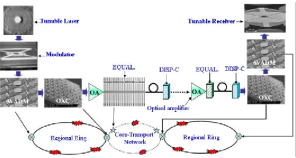
EVICESIn the last few years the wavelength division multiplexing of optical communication has evolved from high-capacity, point-to-point links toward full optical networking. The vision has placed stringent demand on next-generation network elements, such as wavelength agile lasers, reconfigurable add/drop
multiplexers, high port-count mux-demux devices, optical cross-connects, broadband amplifiers, gain and dispersion equalizers, in-line optical spectrum analyzers, high-capacity fiber and elements for network management. MEMS technologies had attracted significant attention in many optical applications. As can be seen above, there are many places in a modern optical communications system where such devices will become the solution of choice. The demonstrated MEMS devices applied in optical communications system include Tunable Lasers [11], Filters [12,13], Gratings [14], Optical Switches [15,16], Gain Equalizer/Attenuator [17,18], Optical Cross Connect (OXC) [19,20], Wavelength Division Add/Drop Multiplexer (WADM) [20],and Tunable Receiver [21,22]. Fig.1.4 shows the relationship of the optical networking and optical MEMS components.
Figure 1.4: MEMS component for optical networking
1.3.1
L
IGHTS
OURCEAt or about the time that DWDM system was finding their way into fiber optic networking back in the mid-1990s. Network operators began realizing that
they were going to have concerns regarding the numbers of lasers that were used in DWDM systems. The problem became more acute as the number of channels grew, first to 32 then 64 and then 80 channels and beyond. The result has been a mad rush by numerous optical components vendors to make tunable lasers, lasers that can be used to replace any fixed wavelength laser across a given band.
1.3.2
O
PTICALS
PECTRALD
IVISIONC
OMPONENTSFilters and gratings have become a key enabler of optical communication. Those potential is enormous that can intelligently route signals through a complicated maze of optical interfaces and still maintain precise location and purity of signal. Optical modulators are integrated components designed to control the amount of continuous optical power transmitted in an optical transmission system. Filters can and will be able to perform these add/drop functions better than any other technology as the number of signals increase and optical switching becomes a real factor in next optical networks.
1.3.3
O
PTICALA
MPLIFIERSThe types of opamps manufactured, EDFAs still make up the vast preponderance of the optical communication because they work best in the C-band (1530-1565nm), which is where DWDM works best and has done most of its networking. However, some new type of amplifier radically improves on the noise and gain characteristics inherent in conventional EDFA technology and significantly lessens the need for regeneration.
1.3.4
O
PTICALP
ATHS
ELECTIONC
OMPONENTSThe optical switch, optical cross connect and wavelength division add/drop multiplexer are called path selection devices. The “large optical switched”, such
as the Tellium and Lucent switches mentioned above are really optical crossconnects. They had been focused on the development for optical communication applications. In the optical fiber networks, a matrix of optical switches, used to bypass failed nodes to reconfigure the network, are needed to preserve the network reliability. In addition, the information exchange is accomplished by switching and routing optics. MEMS technologies provide a solution to manufacture hundreds of optical switches that enable the crossconnect of light signals completely in the optical domain. Moreover, small optical switch (1x2, 2x2…etc.) that is similar in design to the fast add/drop switch but also for optical restoration, protection, test and provisioning applications.
1.3.5
L
IGHTI
NTENSITYC
ONTROLC
OMPONENTSNo uniform signal intensity levels in wavelength division-multiplexed (WDM) communication systems lead to transmission errors. Power equalization can be done by signal pre-emphasis and fixed fiber gratings. However, transmission link properties can change over time, and the network operator may not have precise, dynamic control over source powers. Gain Equalizer and Attenuator providing dynamic control over wavelength power levels could correct changing signal levels with a simple, local control algorithm and provide maximum flexibility to the network operator.
1.4
O
BJECTIVES OFD
ISSERTATIONIn the dissertation, we will focus on the growing demands of fiber optics communication. The main objective of the dissertation is to develop simplified and reliability fabrication methods for optical communication applications. Specifically, different actuator designs for optical communication devices include
tunable filter, variable optical attenuator and dual comb-drive optical switches for optical switch. The objectives of present research work are
(1) Low temperature process developed that can fabricate tunable Fabry-Perot filter and integrate with optical components.
(2) Using SOI-MEMS process designs thermal actuator array that can achieve large displacement for variable optical attenuator.
(3) Self-aligned process developed that can fabricate dual comb-drive optical switches for optical switch and modulator.
The drawbacks of existing fabrication methods to fabricate tunable Fabry-Perot filters include high driving voltage, poor parallelism between two distributed Bragg reflector mirror, complex fabricating processes and uncontrollable or limited of resonant cavity length. Furthermore, the existing fabrication methods were constrained by the substrates, high process temperature and complex fabrication process. In order to overcome the above-mentioned drawbacks, a low temperature surface micro-machined technology that is suitable for fabricating tunable Fabry-Perot filter is proposed. In particular, the present process is not limited by any substrates that can also be integrated to fabricate tunable VCSEL.
According to driving methodologies, optical shutter types or reflective mirror types VOAs that are driven by electrostatic force are able to achieve large displacement with high driving voltage or numerous comb -fingers. The more comb-fingers the larger displacement can be obtained and in return we increase the actuator mass and decrease response time. Existing thermal type VOA device uses the thermal arch beam approach, which is capable of achieving large
displacement with low driving voltage. Unfortunately, its fabrication method is complicated in realization. In order to overcome those drawbacks, a variable optical attenuator fabricated by MEMS-SOI fabrication technology using the newly developed thermal actuator array with dual shutters is developed. The thermal actuator array can achieve larger displacement with low voltage than traditional thermal actuator array.
Optical communication devices may require large deflection angles or large actuation force characteristics with multi-directional/axis motion and good reliability. However, the existing fabricating methods such as bonding technology and reflow photoresist assembly method are so complicated that they can easily produce asymmetric and unreliable driving structures. Moreover, these complicated processes reduce the repeatability and yield for a realistic manufacture. A novel method based on multi-layer SOI process for fabricating a self-aligned electrostatic vertical actuator is developed. The comb fingers using self-aligned process is completed in a successive etching process and simultaneously separate upper and lower electrodes without critical alignment. This not only greatly simplifies the fabrication process, but also provides a solution to create realistic dual comb-drive optical switches.
1.5
O
RGANIZATION OFD
ISSERTATIONThe dissertation is organized as follows. In the Chapter 2, we introduce MEMS fabrication techniques, including of bulk micromaching process, surface micromaching process, and SOI-MEMS process. MEMS sensors and actuators designed using these technologies in practical are presented.
Chapter 3 describes the theories of Fabry-Perot for tunable filter. The characteristics of optics and mechanism are designed and considered for the proposed optical communication application. A low temperature fabrication process is developed for the tunable Fabry-Perot filter. Moreover, the characteristics of the fabricated tunable Fabry-Perot filter are demonstrated.
Chapter 4 introduces variable optical attenuator that consisted of a thermal actuator array, shutter and optical fibers. The mechanical characteristics and simulation of thermal actuator array are presented. The simplified and reliability fabrication process is development. Furthermo re, the characteristics of variable optical attenuators are demonstrated.
In the Chapter 5, a novel of dual directional actuator is illustrated. A self-aligned fabrication method to fabricate the dual comb-drive optical switches is developed. The mechanical characteristics and simulation of dual directional actuators are demonstrated. The developed moveable carriers can be used as tunable components for optical application. Moreover, it has the capability to provide high operation speed with large angle motion for scanning mirror and optical switch.
Finally, we conclude accomplishments of thesis and propose the direction for future in the Chapter 6.
CHAPTER II
MEMS Fabrication Technology
2.1
I
NTRODUCTIONIn the last two decades, the development of micro-electromechanical system (MEMS) technologies has grown dramatically because of their potential applications [23-25]. These MEMS technologies allow us to fabricate various three-dimensional mechanical structures with very small size, which meet the requirements of microsensors and microactuators. Generally speaking, traditional MEMS technologies include bulk micromachining, surface micromachining, and LIGA. Today, commercial products have been well developed and fabricated by combining the full-grown IC technologies with additional, compatible micromachining processes [26, 27]. Moreover, the more potential fabrication technologies have been developed that produces more unusual microstructures with high aspect ratio [28, 29]. The technologies can be used in optics, microfluidics, biochemistry, and aviation. In this dissertation, optical communication devices were designed, developed and assembled through various fabrication technologies that include: bulk micromachining, surface micromachining and SOI-MEMS technology. In this chapter, we introduce these techniques as well as fabricated components for practical application.
2.2
B
ULK MICROMACHINGP
ROCESSIn bulk micromachining, the micromechanical structures are shaped by etching silicon substrate. Generally, bulk micromachining can be classified into
isotropic and anisotropic etching. In isotropic etching, silicon is etched at equal rates on all directions. While in anisotropic etching, silicon is etched at different rates along the different crystal plane. Anisotropic etching techniques provide a high-resolution etch and tight dimensional control due to their high selectivity to different silicon crystallographic orientation [30, 31]. Hence, these techniques are key processes in most MEMS fabricated.
As mentioned above, anisotropic etchants etch much faster in one direction than in another, exposing the lowest etching crystal planes over time. Generally, the etch rate is slowest in the <111> directions, and fastest in the <100> and <110> directions. By using anisotropic etching, various three-dimensional structures can be formed on different oriented wafers, such as (100) and (110) oriented wafers, as shown in Fig.2.1 (a-b). On a (100)-oriented wafer, four sidewalls with an inclination of 54.74o, call V-groove, are shaped along the etch-resisatnt {111} planes. In contrast to a (100) wafer, a (110) wafer creates four vertical walls limited by {111} planes [32, 33].
(b)
Fig.2.1 V-groove cavities are formed by anisotropic etchant (a) (100)-oriented (b) (110)-oriented [32]
The state of the art technique is widely used in MEMS applications for various sensors, actuators and micro-optical applications. Fig. 2.2 shows some microstructures that can be used such as vacuum sensors, printer head, fiber alignment groove and pressure sensors. The most commonly used anisotropic etchants are EDP (ethylenediamine-pyrocatechol-water) [34], TMAH (tetranethylammonium hydraoxide) [35], hydrazine solution [36] and KOH [37]. These etchants can be highly material selective, which indicates that they may be masked by different materials. Typically, oxide, nitride and aluminum films could be used as masking material in hydrazine and Si-added TMAH solution.
Fig. 2.2 MEMS applications using Si bulk micromachining [37]
2.3
S
URFACE MICROMACHINGP
ROCESSEarly demonstrations of potential of surface micromachining were advanced in the 1960s and 1970s by scientists at Westinghouse Electric Corp., and at IBM
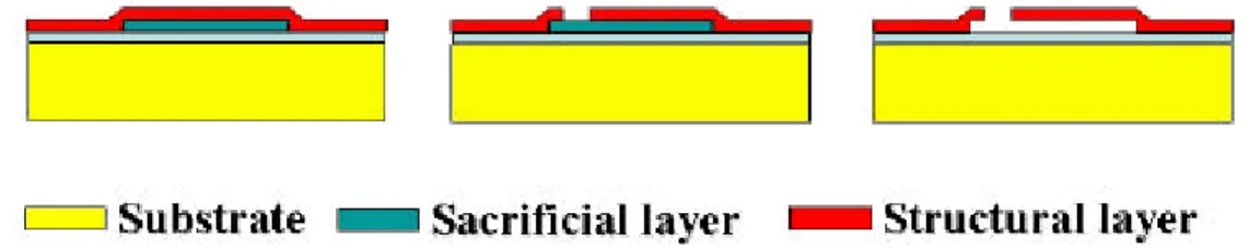
micromechanical switches and electronic filters that use mechanically resonant thin-film metal structures [38]. At IBM, developments centered on the application of surface micromachining principles to displays, mechanical switches and sensors, in which thin-film oxide structures were integrated with microelectronics [39]. In surface micromachining, thin-film material layers are deposited and patterned on a wafer substrate. Thin-film material deposited under a free-standing mechanical structure is called sacrifical material. The material, out of which the free-standing structure is made, is called structural material. To define a given surface-micromachined structure, a recipe of wet etching, dry etching, thin-film deposition and release steps must be composed. The important step in the surface micromachining process is that of dissolving the sacrificial layer to free the structural elements. It has been widely reported to be responsible for greatly curtailing the yield and reliability of the fabricated MEMS devices due to the phenomenon of stiction. There are several terms to evolved stiction problem such as adhesion due to Van Der Waals force, electrostatic force, capillary force and contamination [40]. To improve the stiction problem, MEMS chips are transferred to perform super critical drying process, which can be done through several commercialized CO2 super critical drying machines. Since the molecular state of
the liquid does not form during drying, the capillary problems can be efficiently avoided. Fig. 2.3 shows the key steps involved in surface micromachining.
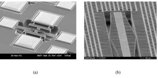
The famous surface micromachining process, Multi-User MEMS Process (MUMPs), was developed at Berkeley Sensors and Actuators Center (BSAC) of University of California in the late 80’s. Since 1992, MUMPs had provided a standard fabrication platform of surface micromachining to MEMS engineers for prototyping MEMS products. It was exploitation of three structural polysilicon and sacrificial silicon dioxide to fabricate free-moving mechanical devices included micromirror and microvalve [41] shown in Fig. 2.4.
(a) (b)
Fig. 2.4 (a) micromirror, and (b) microvalve fabricated by using MUMPs technology [41]
2.4
O
THERE
XISTINGMEMS
P
ROCESSESMajor advances in MEMS fabrication processes in the last few years include polysilicon surface micromachining process [42], deep Si RIE process [43, 44], and the creation of Si-Si wafer bonding processes [44]. Modern equipment for the latter two processes has accelerated research and commercialization of bulk micromachined structures. Other highlighted processes include LIGA (and LIGA-like) plating [45], molding processes, and the recent emergence of silicone (PDMS) molding that can be integrated to realize the models for realistic
Deep etching of silicon has become a key technology in fabricating micro-electro-mechanical systems (MEMS). These structures range in depth from around 10µm up to 500µm. There are several ways of achieving such deep, vertical silicon structures. The most popular techniques are developed by Robert Bosch GmbH, (hereafter referred to as the ‘Bosch’ process) and an alternative process relying on cooling the stage and silicon to cryogenic temperatures using liquid nitrogen [46]. These techniques are in the process of replacing the previously used deep etching techniques, which relied on anisotropic wet chemistry. Dry processing tends not to be sensitive to crystallographic orientation (unlike the wet anisotropic processes) and can have very high selectivity to the masking material. They are also easily automated for production and are considerably safer than the equivalent wet processes. These techniques are finding a wide range of applications within the MEMS market. This process uses a fluorine based plasma chemistry to etch the silicon, combined with a fluorocarbon plasma process to provide sidewall passivation and improved selectivity to masking materials. Sulphur hexafluoride (SF6) is the source gas used to provide the fluorine for silicon etching. The sidewall passivation and mask protection is provided by octofluorocyclobutane (c-C4F8), a cyclic fluorocarbon that breaks open to produce CF2 and longer chain radicals in the high density plasma. A complete etch process cycles between etch and deposition steps many times to achieve deep, vertical etch profiles. It relies on the source gases being broken down in a high-density plasma region before reaching the wafer, which has a small but controlled voltage drop from the plasma. The process widely used form of high-density plasma systems (HDP) uses inductive coupling to generate the high-density plasma region so is known as ‘inductively coupled plasma’ (ICP). Fig.2.5 shows the high aspect ratio trench fabricated by ICP process.
Fig. 2.5 SEM picture of high aspect ratio trench [44]
Perhaps the most prolific research theme in MEMS fabrication is the incorporation of new materials. Slightly tensile polysilicon and low-stress silicon nitride are innovations from the early 90’s. Recent work on thin-film polycrystalline SiGe microstructures is motivated by the low temperature deposition and post-CMOS compatibility. Thin-film SiC structures deposited in molds and planarized with CMP are promising for applications at high temperatures and in harsh environments. ZnO and PZT continue to be explored as MEMS-compatible piezoelectric thin films for actuation and sensing [52]. In particular, with its ease in making high-aspect–ratio channels, SU8 resist has become increasingly popular in combination with glass or silicon bonding [47]. Electroplating and sputter deposition of magnetic materials, including NiFe (permalloy), NdFeB and CoP, are of current interest for use in magnetic field sensing, actuation, and miniature probe-based data storage [48].
Most of these processes can be grouped into several broad areas. Much work is still ongoing on “standard” surface and bulk micromachining. The U.Michigan
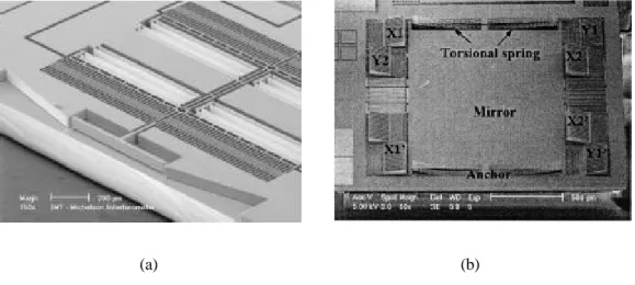
techniques. Molding processes, as mentioned earlier in discussing LIGA, SiC and PDMS structures, are widely used in MEMS. Polysilicon (and silicon nitride) molding techniques, such as the HARPSS process [49], have advantages in making high-aspect structures. Deep Silicon RIE structures are now in widespread use, and several techniques have been offered to provide structural release and electrical isolation. Silicon structures are undercut with an isotropic etch in Cornell’s SCREAM process and interconnect is provided with sputtered metallization on the sidewalls [50]. Fig. 2.6 shows the resonator and accelerator fabricated by HARPSS and SCREAM technology respectively.
(a) (b)
Fig. 2.6 (a) Resonator and (b) Accelerator fabricated by HARPSS and SCREAM technology respectively [49,50]
CMOS micromachining forms structures directly from the CMOS interconnect layers from which complex heterogeneous structures are made from multiple aluminum, polysilicon, and oxide dielectric layers [51]. SOI-MEMS processes have a built-in oxide sacrificial layer, which also functions as electrical isolation [28-29, 43-44]. Alternatively, Silicon bonding processes can first provide a pre-etched pit underneath the microstructures and oxide trench-fill isolation can provide electrical isolation. Carnegie Mellon’s CMOS-MEMS process has been
recently extended to incorporate DRIE Silicon, where interconnect is provided through thin films on top of the Silicon structures [50]. Polysilicon hinge technology with electrostatic assembly is fairly advanced, and is primarily used in micro-optics applications. Bendable metal hinges with electromagnetic assembly have also been demonstrated. Fig. 2.7 shows the variable optical attenuator and torsion mirror fabricated by SOI-MEMS and CMOS-MEMS technology respectively.
(a) (b)
Fig. 2.7 (a) Variable optical attenuator and (b) Torsion mirror fabricated by SOI-MEMS and CMOS-MEMS technology respectively
2.5
S
UMMARYIn this chapter we introduce the origin of motivation behind the development of MEMS fabrication techniques included surface micromachining, bulk micromachining, LIGA and other potential MEMS fabrication technologies. Current and future research thrusts can be grouped into three areas: material improvement, process integration, and manufacturability. Novel equipments have accelerated research of fabrication techniques and commercialization of MEMS components. Note that the advantages of MEMS are batch fabrication at low unit
information processing.
In the following chapter, we will integrate above-mentioned of the reviewed fabrication technologies to fabricate several MEMS devices included tunable Fabry-Perot filter, variable optical attenuator and dual directional vertical actuator for optical communication applications.
CHAPTER III
WAVELENGTH SELECTION DEVICE: TUNABLE
FABRY-PEROT FILTER
3.1
I
NTRODUCTIONThe function of an optical spectral filter is to recognize a narrow band of frequencies from a multiplicity of either pass it or reject it. It is the key component in optical transmission systems in general. Optical spectral filters are developed based on interference, diffraction or absorption that can be used in the fixed and in tunable forms. Specifically, the Fabry-Perot filter consists of two high-reflectance multilayers separated by a half-wavelength space layer. Multiple interference in the space layer causes the filter output spectral characteristic to peak sharply over narrow band of wavelengths that are multiples of theλ/2 spacer layer. In general, there are different methods and concepts to fabricate tunable Fabry-Perot filters using micro-electro-mechanical systems (MEMS) technology [53-59]. In this chapter, we focus our study on theory, design, fabrication, and measurement of surface micromachined tunable Fabry-Perot filters.
3.2
T
HEORY OFF
ABRY-P
EROTR
ESONATORAn optical resonator traps and confines light of certain wavelengths and operate like an optical transmission system incorporating feedback: light circulates or is repeatedly reflected within the system without escaping. The simplest resonator is composed of two parallel mirrors between which light is
A plane wave of complex amplitude Ui and intensity Ii which enters a planar-mirror resonator undergoes multiple reflections and transmissions, as illustrated in Fig. 3.1.
(
Ui: amplitude of input light ; Ut: amplitude of outgoinglight ; r1,r2: reflection coefficient; t1, t2: transmission coefficient; d: resonator cavity length; λ: wavelength; n is integer)
Fig. 3.1 Transmission of a plan wave across a planar-mirror Fabry-Perot resonator
In a resonator with losses, the excursion of the wave U0 between the two
mirrors results in an infinite sum of phases. The phase difference after at both mirrors is: m v vd d k π ϕ = 2 =4 (3-1)
k is the wave number and vm is the speed of light in the medium. Due to
non-perfect mirror reflections and absorption in the medium an effective mirror reflectance is represented by R=r2. Considering U1=hU0, where h =Re−jϕ and
the phase U2 are related to U1 by this same complex factor h. The intensity in the
) 2 ( sin ) 2 ( 1 ) 2 ( sin 4 ) 1 ( Re 1 2 2 max 2 2 2 2 2 ϕ π + = ϕ + − = − = = ϕ − F I R R Ii U U I j i t (3-2)
The equation is call the Airy transmission coefficient, whereImax = Ii/(1−R)2; and I0 is the intensity of the initial wave.
The most important parameters to characterize the spectral response of the FabryPerot resonator are: finesse (F), full-width falf-maximun (FWHM), free spectral range (FSR) and resolving power (ℜ), which will be described in detail and shown in Fig. 3.2 following.
Fig. 3.2 Transmission peaks are equally spaced as a function of frequency.
Narrow peaks are formed in transmission. The sharpness of the peaks increases with increasing reflectivity. FWHM is the width of the peaks at half-height. Finesse is as the ratio of the separation of successive peaks to the peak width at half-intensity [60, 61]:
R R F − = 1 π (3-3)
.The spacing between adjacent resonance frequencies is called the free spectral range. Generally, the FSR is the wavelength range over which the spectrometer can measure unambiguously. FSR is defined as:
d FSR 2 2 λ = (3-4) In a tunable Fabry-Perot the free spectral range and the FWHM bandwidth can be controlled independently. The cavity gap sets the free spectral range, and mirror’s reflectivity controls the finesse. The transmission peaks can be made very sharp by increasing the reflectivity of the mirror. The resolving power (ℜ) is the ratio of λ0 to the least resolvable wavelength difference. It is obtained by:
) 1 ( 2 ) 1 ( 0 0 R R d n R R q FWHM f − = − = = ℜ λ π λ (3-5)
According to the above-mentioned function, a suitable optical resonator length and high reflectance of distributed Bragg reflector mirror are the most important parameters in designing a high quality Fabry-Perot filter. In the present proposed process, the designed device consists of 1.6um optical resonator length and mirrors have a reflectivity of about 99.5%. Note that the calculated theoretical FSR is about 750nm and FWHM is close to 1.2nm.
3.3
O
PTICALD
ESIGN OFF
ABRY-P
EROTF
ILTER3.3.1
D
IELECTRIC MIRRORS DESIGNThe most important part of the Fabry-Perot device is the mirrors. Two types of highly reflective coatings are used: dielectric and metallic. The deposition of a sequence of two different dielectric films of well-controlled thickness must to
form a stack of many layers. The performance of the filter is greatly influenced by random thickness variations in the deposition of the films. To be effective in a wide optical band, a dielectric mirror must consist of multilayer. It is best to measure the refractive index and the extinction coefficient of layers produced by the process.
The multilayer structure is arranged in succession and characterized by the sequence HLHL… HLH. The characteristic matrix of this multilayer now is 2N+1 layers, where N is the number of times HL is used. With n1, nH, nL as the refractive
indexes of air, the layer with high n and lower n, respectively. This leads to the reflectivity [62]: 2 2 2 1 2 2 1 1 2 ) ( ) ( 1 ) ( ) ( 1 + − = + N L H H N L H H N n n n n n n n n R (3-6)
This last expression indicates the reflectivity increases rapidly with both the ratio nH/nL andN. The structure of mirrors composes of 3.5 pairs of Si and SiO2
where the thickness is about 1076A and 2672A respectively. The mirrors have a reflectivity of about 99.5% from approximately 1.35um to 1.6um as measured in Fig.3.3.
3.3.2
M
ETALLIC MIRRORS DESIGNAlthough the metallic-based coatings have much higher losses than dielectric-based coatings, these can be attractive in certain applications due to the simplicity of their fabrication. Another advantage is that metallic mirrors generally perform well over a wide spectral range. Aluminum, gold and silver are
the most commonly used metals for reflective coatings. Fig.3.4 shows their reflectance in the near-UV, visible and near-IR spectral region [63]. Unfortunately, Fabry-Perot filters using metallic mirrors cannot provide both high finesse and high transmittance simultaneously, due to optical absorption in the metal.
Fig. 3.3 Reflectance of Si/SiO2 as a function of the wavelength.
3.3.3
O
PTICAL SPECTRAL SIMULATIONA Fabry-Perot resonator composes of 3.5 pairs of Si and SiO2 layers on both sides with an air gap of 1.6um. It was used as a simulation parameter to build the graph presented in Fig. 3.5. This information enabled us to investigate transmittance wavelength by varying the cavity gap. Fig. 3.6 shows the simulation of the spectrum in the C band (1528-1561nm) with 20 channels.
Fig. 3.5 The relationship of the variable gap and transmittance wavelength
3.4.
F
ABRICATIONP
ROCESSThe schematic Fabry-Perot filter structure is shown in Fig.3.7. The proposed filter consists of an optical mirror on silicon substrate and a floating bridge structure with another optical mirror that is formed on top of floating bridge. The electrostatic force is used to adjust the optical resonator length with a driving voltage that is applied to the top and the bottom electrodes in order to tune needed resonant wavelength. According to the optical transmission characteristics, when the air gap equals multiplicity of a half wavelength of the incident broadband light, which will enable to filter the suitable wavelength with a sharp resonant transmission peak passing through the two parallel mirrors. The optical resonator length of the device is designed for a center wavelength of 1550nm.
In order to realize the proposed optical filter, a new low temperature fabrication process is summarized in Fig.3.8 (a)-(f). First, we deposited titanium to isolate the useless light and patterned an aperture to force light pass through it. Next, the bottom mirror was deposited on titanium isolator as shown in Fig.3.8 (a). In Fig.3.8 (b)-(c), we deposited and patterned titanium as the bottom electrodes, then deposited aluminum to be the sacrificial layer. Note that the critical issue of the present processes is the use of aluminum that is standard material used in IC process. Note that the material properties and parameters of deposition rate of aluminum have been completely understood which can be used to control its thickness accurately for optical resonator length. E-gun was used here to deposit the sacrificial layer and to ensure the design requirements could be matched accurately. With the lower mirror and the sacrificial layer, we further used E-gun to deposit seven overlapping layers of Ti/Au layers, which are 1000 A0, and 8000
with any existing optical processes that can be used to form the bridges and membrane. The purpose of using Ti/Au layers is to compensate its individual material stiffness properties. Furthermore, in order to eliminate the residual stress between the layers, we place the fabricated filter in the N2 gas chamber at 200 0C
for 30 minutes to complete its annealing process. As shown in Fig.3.9, we observed the difference between the released bridges with or without the residual stress due to annealing. In the Fig.3.8 (e), we completed the deposition of the top mirror using left–off technology. To obtain the final Fabry-Perot filter, aluminum-etching solution is used to release the sacrificial layer as shown in Fig.3.8 (f). However the aluminum-etching solution also attacks titanium electrode resulting in the disappearance of top and bottom electrodes. Nevertheless, in order to avoid the etching of titanium, dissolving a grain of aluminum into the etching solution for a few minutes that would dramatically decrease the titanium-etching rate. Finally, we used methanol and hot plate to avoid the sticking phenomenon between membrane and substrate. It is note that the best method to avoid the sticking phenomenon is to use CO2 critical point
dryer. Note that all of the processes were fabricated by physical vapor deposition implying that if there have been existed photonic devices on substrate; the low temperature processes would not affect these devices.
Fig.3.8 (a)-(f) Summary of the fabrication process
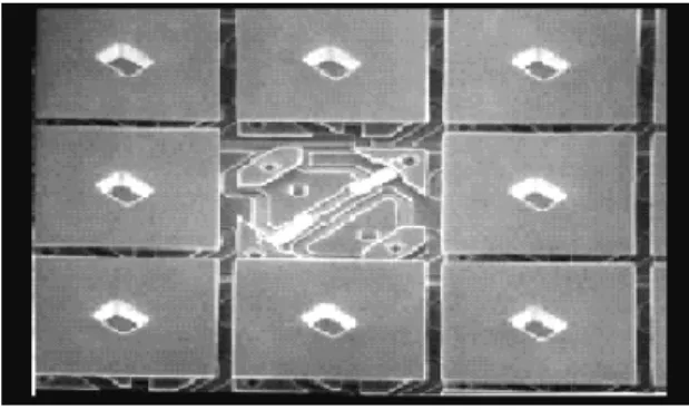
Fig.3.10 SEM picture of the Fabry-Perot filter
Fig. 3.10 is the SEM picture of the Fabry-Perot filter with membrane area of 200um ×150um. The top and bottom mirror are circles in the center of the membrane with a diameter of 100um and on the substrate with a diameter of 120um respectively. These mirrors compose of alternating λ/4 layers of Si and SiO2 for the reason that they have large index contrast property and they are
common materials used in semiconductor fabricating process. The structure of DBR composes of 3.5 pairs of Si and SiO2 where the thickness is about 1076A
and 2672A respectively.
3.5.
E
XPERIMENTALR
ESULTIn the present experimental setup, the ASE light was used as broadband light source in the 1550nm region to verify the fabricated Fabry-Perot filter. The light beam was going through the fiber and collimator and lead into Fabry-Perot filter.
individual transmission wavelength. The output light is collected by a lens transmitted through a multimode optical fiber and guided it to an optical spectrum analyzer ADVANTEST Q8347 for spectrum measurements. Fig. 3.11 shows the relationship between the wavelength output (1532nm-1542nm) and the bias voltage (0-30 volts) of the fabricated Fabry-Perot filter. The reason that we need a high bias electrostatic actuated voltage is due to the small electrode area.
Fig.3.12 demonstrates the relationship between light intensity and wavelength. Here in the 10nm range, we are able to tune 5 output wavelength channels where the FWHM of the output wavelength peak is about 1.3 nm. This result matched the theoretical data closely.
However, the transmission wavelength intensity (15-20%) is not performed well as our anticipating. This is due to the reasons that: the membrane may tilt slightly during the stage of applying the driving voltage to the membrane and consequently loss the incident-light intensity. Furthermore, since the fabricated Fabry-Perot filter does not coat with anti-reflection layers on the backside of the wafer, which may produce a decayed light intensity through wafer. Fig.3.13 indicated that the residual stress of DBR mirror would produce 0.225um average flatness error. This error is larger than λ/4 of the light source from Zygo interferometer which affect the light intensity in our experiment with ASE light source. In conclusion, the overall performance of the filter is strongly affected by the above-mentioned behaviors.
3.6.
S
UMMARYIn this chapter, a ultra-low temperature (< 200 ℃) fabrication process for micro-machined tunable filter has been proposed with proven feasibility. With the low temperature property, the process could be used to suit different substrates and their detected spectrum is not limited by any substrates although our device is fabricated on silicon substrate here. Note that the present process is compatible with any existing optical or IC process. The fabricated tunable Fabry-Perot filter based on a high reflectance DBR, which is up to 99%, low stress membrane, and suitable driving voltage that produced a small FWHM of 1.3nm. This low temperature MEMS process has the potential to integrate with other existing photonic devices such as tunable VCSEL. Moreover, a high quality Fabry-Perot filter could be used as a key component of interferometer or spectrometer.
In this next chapter, a variable optical attenuator using thermal actuator is introduced. A simplified fabrication method and high yield is proposed and demonstrated.
Fig. 3.12 The tuning wavelengths versus intensity
(a)
(b)
![Figure 1.1 Poly-Si micromotor [2]](https://thumb-ap.123doks.com/thumbv2/9libinfo/8448423.182339/1.892.272.653.621.869/figure-poly-si-micromotor.webp)
![Fig. 2.2 MEMS applications using Si bulk micromachining [37]](https://thumb-ap.123doks.com/thumbv2/9libinfo/8448423.182339/14.892.250.678.639.926/fig-mems-applications-using-si-bulk-micromachining.webp)
![Fig. 2.5 SEM picture of high aspect ratio trench [44]](https://thumb-ap.123doks.com/thumbv2/9libinfo/8448423.182339/18.892.252.643.110.430/fig-sem-picture-high-aspect-ratio-trench.webp)