Abstract
Field emission display is evolving as a promising technique for the future generation of flat panel displays. Characteristics affecting the power of field emitter arrays include the shape and work function of emission materials, distance between tip and gate, and the environmental vacuum condition.
In this work, we present a novel scheme that involves a new fabrication process of gate structure metal–insulator–semiconductor (MIS ) diode using IC technology. Deposition of the diamond film in this MIS diode forms a column-like diamond with gated field emission arrays ( FEAs). This process is completed using a bias-assisted microwave plasma chemical vapor deposition system. Our results indicate that the threshold voltage of column-like diamond FEAs is about 10 V, and the field emission current density is about 139 mA cm−2 (at Vgc=20 V ). The diamond field emitter array devices with the new gate structure and tip morphology significantly influence the electron field emission characteristics. © 2000 Elsevier Science S.A. All rights reserved.
Keywords: Emission current; Field emission arrays; Flat panel displays
1. Introduction plasma chemical vapor deposition, in which the process
is successfully completed. Field emission devices (FEDs) with a high emission
current density have been developed in metal tip [1] and silicon tip arrays [2]. Having great potential as electron
2. Experimental emitters in flat panel displays, the devices have attracted
much attention. However, the electrical field required to
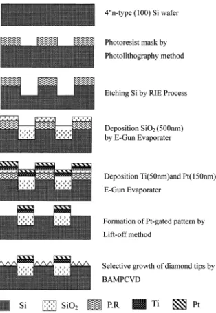
Fig. 1 illustrates the detailed process sequence for trigger field emission is rather high and the FED’s
forming of a triode diamond tip array with a Pt gate. performance declines rapidly as a result of thermal
First, we designed the metal–insulator–semiconductor effects, resulting in serious contamination of, and
(MIS) diode structure and fabricated the MIS diode damage to, the emission material.
using semiconductor process technologies. Starting sub-Diamond films possess negative electron affinity, and
strates were mirror-polished n-type, (100)-oriented wafers useful properties such as high electron mobility
with a resistivity of 4–6 V cm. The silicone wafer was (2.2×103 cm2 V−1 s−1), high thermal conductivity
first cleaned by an RCA cleaning process. It was then (20 W cm−1 °C−1) at room temperature, high
break-covered with FH-6400 positive photoresist, using a spin down threshold voltage (107 V cm−1), and chemical
coater. Next, a set of arrays of circle-shaped patterns was inertness. It also exhibits a rather high field electron
UV exposed and developed in the resist layer. velocity (2.7×107 cm s−1) which increases the maximum
After formation of photoresist patterns, an RIE emission current that can be attained before saturation.
system (model Samco RIE-10, Japan) was used to etch Therefore, diamond films are considered to be very
the silicon layer at a depth of 300 nm. When the RIE useful in electron FEDs and their related emission
system produced a hole with a depth of 300 nm depth, properties have been widely investigated [3–5].
a dual e-gun evaporator (model ULVAC EBX-10C, Accordingly, this work fabricates field emission array
Japan) deposited silicon dioxide (SiO2) to a thickness of ( FEA) devices in diamond by bias-assisted microwave
500 nm. Next, the adhesion between the Pt layer and the SiO
2layer was increased by sequential deposition of * Corresponding author. Fax:+886-3-5723811.
E-mail address: [email protected] (Chia-Fu Chen) the Ti (titanium) and Pt (platinum) layers, with thick-0925-9635/00/$ - see front matter © 2000 Elsevier Science S.A. All rights reserved.
Fig. 2. The scheme of the instrument for the I–V measurement.
rotary pump. Initially, the reactant gas, hydrogen, was introduced into the chamber at a rate of 200 sccm to clean the substrate by the following hydrogen plasma. The reactant gas pressure was set at 15 Torr. Microwaves were introduced at a power of 300 W and, in doing so, a bright plasma was obtained. Next, a negative bias voltages of 80, 120 or 170 V was applied. Under these conditions, a substrate temperature of 650–680°C was obtained. At this stage, the reactive gases were intro-duced into the system. The reactive gases used in depos-ition were the conventional mixture of CH4 and H2.
All the experiments involving the diamond deposition Fig. 1. Fabrication procedure of a triode diamond tip array.
used two-step depositions. The flow rate CH4/H2 and the deposition time of the first step remained constant at 10/200 sccm and 30 min, respectively. Deposition nesses of 50 and 150 nm, respectively, as gated layers
using the evaporator. After the gated layers ( Ti and Pt) typically lasted for 30–60 min. Table 1 summarizes the experimental conditions. Scanning electron microscopy were formed, the photoresist mask was removed with
an acetone solution in an ultrasonic agitator. The (SEM ) was used to observe the morphology of column-like diamond FEAs with a gated structure. A Hitachi Pt-gated circles, have diameters of 4 mm, were formed
by a lift-off process. The sample was then placed into S-4000 scanning electron microscope was used in our experiments. The column-like diamond was qualitatively the chamber of the bias-assisted microwave plasma
chemical vapor deposition (BAMPCVD) system to analyzed by laser micro-Raman spectroscopy (Renishaw, Model 2000). Auger electron spectroscopy obtain the diamond tips. The BAMPCVD chamber was
then evacuated to a pressure of ~0.01 Torr with a (AES ) was used to identify the surface compositions of Table 1
Diamond deposition conditions
Negative bias Deposition time Flow rate of Operating pressure Microwave Substrate voltage ( V ) (min) CH
4/H2(sccm) ( Torr) power ( W ) temperature (°C) First step conditions
A 80
B 120
C 170 30 10/200 15 300 ~660
D 120
E 120
Second step conditions
A 80 2/200
B 120 2/200
C 170 30 2/200 15 300 670–680
D 120 1.4/200
(a)
(b)
(c)
I II
Fig. 3. (a) SEM photographs of triode diamond FEAs grown under conditions A at different magnitudes: (I) 8K; (II) 60K. (b) SEM photographs of triode diamond FEAs grown under condition B at different magnitudes: (I) 8K; (II) 60K. (c) SEM photographs of triode diamond FEAs grown under conditions C at different magnitudes: (I) 8K; (II) 60K.
the column-like diamond. Fig. 2 presents the field emis- were maintained at positive potentials to allow the device to be turned on.
sion properties of the column-like diamond FEAs with a gated structure. These properties were measured using a triode technique. An anode plate (ITO Glass, MBC
6R1697) was placed 1 cm above the Pt gate and was 3. Results and discussion biased to +1000 V. The anode current (I
a) was then
measured as a function of the gate-to-cathode bias A previous investigation has indicated that, when the carbon active species in the plasma were accelerated to voltage in a vacuum of 1×10⁻⁶ Torr using a Keithley
SMU 237. Next, the gate-to-cathode voltage (Vgc) was the silicon substrate by the high negative voltage to form sp2, non-crystalline clusters, some clusters trans-biased from 0 to 30 V using a HP-4145 system. During
testing, the device was in a common emitter configura- formed into sp3 clusters through the collision of carbon species and subsequently formed diamond nuclei sites tion with the grounded emitter. The anode and gate
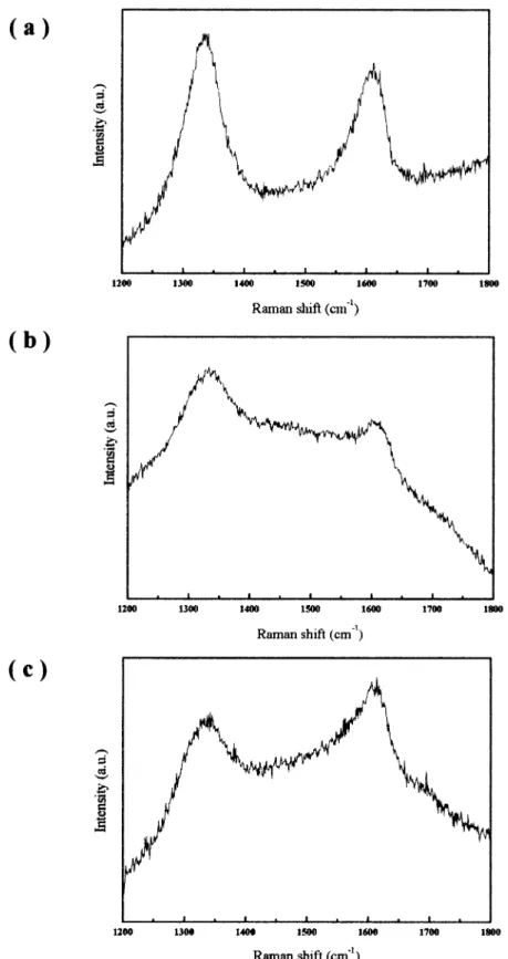
Fig. 4. Raman spectra of samples grown at different methane concentrations in the second step: (a) condition D, 0.7 vol.%; (b) condition B, 1 vol.%; (c) condition E, 2 vol.%.
[6 ]. The other sp2 clusters could be found near these in plasma were accelerated to the silicon substrate by the bias voltage to remove the lower energy sp2 clusters diamond nuclei sites, which have lower activation energy
80, 120 and 170 V negative bias voltage, respectively. The diamonds’ density, size and irregularity of shape increase with the bias absolute voltage. Also, bias-enhanced nucleation and the plasma etching effect can be observed [9]. Moreover, the column-like feature is more obvious with an increased bias.
Fig. 4 displays the micro-Raman spectra for the column-shaped diamond on the Pt-gated FEAs: D, B and E deposition conditions grown at different methane concentrations in the second step of the deposition process. Both the significant peaks at 1332 and 1580 cm−1 appeared in the Raman spectrum. Therefore, the full width at half-maximum (FWHM ) of the dia-mond peak (near 1332 cm−1) increased with an
increas-ing CH4 concentration. This result is characteristic of Fig. 5. The AES spectra of samples grown at different methane concen-trations in the second step: (a) condition D, 0.7 vol.%; (b) condition an amorphous carbon phase with sp2 bonds.
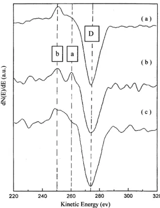
B, 1 vol.%; (c) condition E, 2 vol.%. The AES fine structure taken from the conditions D,
B, and E in Fig. 5 reveals the peak region of the intensity
mond FEAs. The field emission current (I
a) of column-profile of the C KLL peak, indicating that the carbide
like diamond FEAs (condition B in Table 1) is about is formed during the diamond deposition with a negative
44 mA (at gate-to-cathode voltage, Vgc=20 V), the emis-bias. Notably, low-energy shoulders around 258–260 eV
sion current density (Je) of column-like diamond FEAs (peak a) and 248–250 eV (peak b) appear in the spectra
is 139 mA cm−2. Therefore, the higher emission current of the column-shaped diamond under conditions B and
density in the column-like diamond FEAs accounts for D. Their appearance suggests that the surface structure
the gate structure (short gate–tip spacing and small gate is a diamond structure with a few graphite, amorphous
aperture) or the diamond morphology. The threshold carbon and/or other defects [10]. However, AES spectra
voltage (Vth) is defined as the intersection of the F–N of the sample deposited under condition E exhibit no
plots with the abscissa. The threshold voltages (Vth) were obvious peak a, implying a diamond-like carbon
com-around 10 V for column-like diamond FEAs. position including a large amount of graphite,
amor-Owing to the smaller gate aperture diameter and phous carbon and/or other defects.
shallower gate aperture, a field emission current can be CVD diamond and diamond-like carbon films show
triggered at a lower threshold voltage. However, a stable electron emission in a low field. Nevertheless, the
saturated current occurs at V
gc=20 V in column-like nature of electron emission from these materials is still
diamond FEAs. This current is attributed to the fact unclear. Related approaches have attempted to explain
that the SiO
2 layer of the FEAs pattern is probably the ultralow emission fields: negative electron affinity
broken when the FEAs pattern in the BAMPCVD effects available for diamond surfaces including
diamond process, thus increasing the leakage current n-doping and defect levels in the diamond band gap;
from the SiO
2 layer. Therefore, the emission current hot electron transport in interfaced structures; grain
decreases for the column-like diamond FEAs, when the boundary effects; and the effect of geometric field
SiO2 layer has been broken during the BAMPCVD enhancement by morphology protrusions or narrow,
diamond process, particularly if the bias exceeds 120 V. conductive grain boundaries between insulating grains
[11]. The field emission currents do not differ markedly
4. Conclusion from each other with respect to the change of methane
contents for the second step of the diamond deposition
process in column-like diamond FEAs. Fig. 6 shows the In this work we fabricated a new structure MIS diode to triode diamond FEAs for decreasing the turn-on electron emitting characteristics of the column-like
dia-the silicon substrates was successfully achieved using a patterned Pt-gated layer as a nucleation inhibitor in the new structure MIS diode. A diamond tip with a new column-like shape was obtained. Many par-ticle-caps were placed on the top of the tip, using the BAMPCVD system. SAD column-like triode dia-mond FEAs possess field emission properties appro-priate for application as electron emitters in a flat panel display.
3. Characterizing the electrical properties of the column-like triode diamond FEAs with a new gated structure reveals that the field emission current density is about 139 mA cm−2 ; the threshold voltage is about 10 V and lower than that of the metal tip. The results follow from the effect of a gate aperture, the distance between a diamond tip, and the tip morphology. 4. The field emission current of the column-like triode
diamond FEAs might become higher when the dia-mond deposition bias is higher so that a bulkier diamond tip can be obtained. Future work must solve the problem of the quality of the SiO
2 in our new MIS diode process. Therefore, the SiO2 can resist the high field in the BAMPCVD diamond process.
Acknowledgement
The authors would like to thank the National Science Council of the Republic of China for financially support-ing this research under Contract No. NSC88-2216-E-009-020.
References
[1] C.A. Spindt, I. Brodie, L. Humpnrey, E.R. Westerberg, Electrical properties of thin-film field emission cathodes with molybdenum cones, J. Appl. Phys. 47 (2) (1976) 5248.
[2] G.G.P. Van Gorkon, A.M.E. Hoeberechts, J. Vac. Sci. Technol. B 4 (1986) 108.
[3] W.A. de Heer, A. Chatalain, D. Ugarte, Science 270 (1995) 1179. Fig. 6. The electron emitting characteristics of the column-like dia- [4] V.V. Zhirnov, E.I. Givargizov, P.S. Plekhanov, J. Vac. Sci. Tech-mond FEAs (condition B in Table 1). (a) The field emission current nol. B 13 (1995) 418.
(I
a) of column-like diamond FEAs; (b) the emission current density [5] N.S. Xu, Y. Tzeng, R.V. Latham, J. Phys. D 26 (1993) 1776. (J
e) of column-like diamond FEAs; (c) the threshold voltages (Vth) of [6 ] H. Maeda, M. Irie, T. Hino, K. Kusakabe, S. Morooka, J. Mater.
column-like diamond FEAs. Res. 10 (1995) 158.
[7] R. Stochel, K. Janischowsky et al., Diamond Relat. Mater. 5 (1996) 321.
voltage and enhancing the emission current density. [8] D.N. Belton, S.J. Schmieg, Thin Solid Films 212 (1–2) (1992) 68–80.
Results presented herein can be summarized as follows.
[9] C. Hata, M. Kamo, Sato, Plasma etching, New Diamond 12 1. The proposed scheme involving a new fabrication
(1989) 12. process of triode diamond FEAs is feasible. The new
[10] T. Ando, S. Inoue, J. Chem. Soc., Faraday Trans. 89 (4) (1993) MIS diode has a small gate aperture and shallow 749.
field emission cells. [11] A.V. Karabutov, V.D. Frolov, S.M. Pimenov et al., Diamond Relat. Mater. 8 (1999 ) 761–763.