C.C. Wei, P.C. Liu, and Chih Chena)
Department of Materials Science and Engineering, National Chiao Tung University, Hsin-chu 30010, Taiwan, Republic of China
K.N. Tu
Department of Materials Science and Engineering, University of California at Los Angeles, Los Angeles, California 90095-1595
(Received 9 February 2008; accepted 16 April 2008)
Electromigration at 5 × 10⁴A/cm2and 100 °C was conducted to grow composite Pb/Sn whiskers from SnPb solders, in which a Pb whisker grows first and then a whisker of Sn grows. In some cases, small Sn islands are embedded in Pb whiskers. The diameter of a composite whisker is <1m, which is much smaller than that of spontaneous Sn whisker growth on leadframes. The growth orientation of Pb whiskers was in the [110], [11¯1], and [112] directions. This investigation proposes that
compressive stress generated by electromigration at the anode provides the force driving whisker growth. Therefore, accelerated tests of whisker growth at higher temperatures using electromigration are feasible.
I. INTRODUCTION
Spontaneous Sn whisker growth is a serious reliability concern in devices that must be highly reliable, such as satellites1,2because shorting caused by a single whisker can cause a device to fail. In the past, spontaneous Sn whisker growth in solder has typically been prevented using SnPb alloys. Notably, Pb is added to mitigate Sn growth because Pb is soft and can reduce compressive stress quickly.3No composite whisker of Pb and Sn has ever been identified. The SnPb alloy has a lamellar mi-crostructure such that the path along which Sn must dif-fuse for Sn whisker growth can be interrupted by Pb. This study investigates the growth of whiskers in SnPb alloys under a strong driving force and the kinetics of diffusion associated with electromigration. The observed growth of composite Pb/Sn whiskers in SnPb solder al-loys demonstrates that Pb prevents only the growth of spontaneous Sn whiskers and not whisker growth in gen-eral. This experimental finding provides an approach for generating composite whiskers.
Whisker growth can be spontaneous under compres-sive stress in soft metals such as tin, indium, antimony, zinc, and cadmium.4–10 Compressive stress has been measured using focused micro x-ray diffraction in syn-chrotron radiation.6Sn whiskers can grow spontaneously
in a very narrow range of temperatures, ranging from room temperature to roughly 60 °C. At temperatures lower than room temperature, atomic diffusion is insuf-ficient, whereas at temperatures higher than 60 °C, the driving force is insufficient for whisker growth because of stress relief. Indeed, accelerated tests are lacking be-cause the temperature range for whisker growth is so narrow. Whisker growth driven by electrical current in short Sn solder stripes and lines has been investi-gated.11,12In this study, a focused ion beam (FIB) was utilized to fabricate short stripe of SnPb solders and pre-pare a cross-sectional specimen for analysis by transmis-sion electron microscopy (TEM). Composite whiskers were grown by applying a high-density current. Whisker microstructure was analyzed by scanning electron microscopy (SEM) and TEM.
II. EXPERIMENTAL
The SnPb solder strips of various lengths were pre-pared, each about 2.3 m thick. Details of this process are described elsewhere.13Eutectic SnPb solder was re-flowed on a 0.4-m-thick Cu film at 210 °C for 4 s on a hot plate. The sample was then polished to obtain a flat, smooth surface. The final thickness of the solder strip was controlled by polishing. Samples were then annealed at 150 °C on a hot plate for 5 h to remove solder damage caused by FIB etching and polishing. After reflow and solid-state aging, the composition of the solder alloy may vary from the eutectic composition.
Figure 1 shows a cross-sectional schematic illustration a)
Address all correspondence to this author. e-mail: [email protected] DOI: 10.1557/JMR.2008.0253
of the test sample, which is also known as the Blech structure. The continuous layer of Ti metal is the under-lying metal line that conducts current. The arrows indi-cate the directions of electron flow (Fig. 1). Because the solder layer has the lowest resistance in the test structure, most applied current detours into the SnPb solder strips of various lengths. Under a constant applied current, 80% of the applied current drifted into the solder strip, 19% into the Cu–Sn intermetallic compound layer, and only 1% into the Ti layer, based on the resistances of Ti, Sn–Cu compounds, and the solder. The applied current density was 5× 10⁴A/cm2at 100°C. The change in strip morphology was observed by SEM in backscattered im-age mode. Notably, FIB (FEI Nova 200, Hillsboro, OR) was utilized to cut thin slices of whiskers for analysis using a Philip Techni 20 TEM (Eindhoven, The Nether-lands). The microstructure and orientation of whiskers were examined by TEM.
III. RESULTS AND DISCUSSION
Figure 2(a) shows fabricated samples with lengths of 5, 10, 15, and 270m. The length for the trenches be-tween two neighboring solder strips was 10m. Com-pressive stress was generated at the anode end of each segment during electromigration.14
Current-induced compressive stress was used to drive whisker growth. A previous TEM observation demonstrated that no Cu film remained after the reflowing process and no further Cu– Sn reaction proceeded after samples were fabricated.15
Figure 2(a) shows the surface morphology of the SnPb solder strip before current stressing. The Pb-rich phase was segregated on the surface after solid-state aging. The reason for phase segregation may be attributed to thermomigration as the surface of the sample was cold, and it has been demonstrated that Pb atoms migrate to the cold end.16,17 After the sample had been stressed by a current density of 5 × 10⁴ A/cm2 at 100°C for 105 h, many whiskers grew from the strips [Fig. 2(b)]. Notably, in the literature, a whisker growth temperature of 100°C is the highest for PbSn solder. Whiskers grew on the anode end of the strips; most were Sn whiskers, but some were composite Pb/Sn whiskers. The arrows in Fig. 2(b) indicate long Pb/Sn composite whiskers. A Pb whisker grew first, followed by an Sn whisker. If the current density had been low, no whiskers would have formed;
only hillocks would have formed on the anode end of some long strips. Figure 2(c) presents another specimen stressed by a current density of 2× 10⁴
A/cm2at 100°C for 490 h. No whisker was found, suggesting that a threshold-current density or driving force for whisker growth exists. The Joule heating in solder stripes is not serious, since the Si substrate conducts heat well. A pre-vious experimental result for Joule heating for similar structures showed that the temperature increase at the
FIG. 1. Cross-sectional schematic structure for the test sample; arrows indicate electron flow directions.
FIG. 2. Tilt-view backscattered SEM image of surface morphology of SnPb solder strips: (a) after annealing at 150°C for 5 h prior to current
stressing, (b) after being stressed by a current density of 5× 10⁴A/cm2 at 100°C for 105 h (arrows indicate composite Sn–Pb whiskers),
and (c) after being stressed by a current density of 2× 10⁴A/cm2at 100°C for 490 h (no whiskers grew).
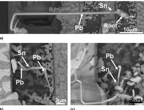
FIG. 3. Various morphologies of composite whiskers grown by current stressing: (a) Pb whisker with an Sn island; (b, c) Sn–Pb composite
whiskers with small diameters of approximately 0.2m.
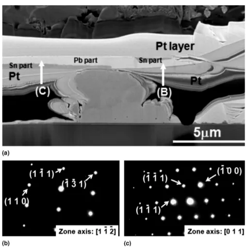
FIG. 4. (a) Backscattered SEM image for a composite whisker grown in a trench between two neighboring solder strips. (b) Secondary-electron FIB image shows the cross-sectional morphology of the whis-ker in (a).
FIG. 5. (a) Cross-sectional TEM image of the composite whisker in Fig. 4(b) showing the interfacial structure of Pb/Sn whiskers. (b) An enlarged TEM image of the Sn–Pb interface in (a).
applied current densities may be only a few degrees cen-tigrade.15
Compressive stress at the anode end generated by elec-tromigration may provide the force driving composite whisker growth. Chen and Wilcox showed that, using the bending stripe method, whiskers grown on tin-manganese films have a tensile stress.18However, no mechanism of spontaneous Sn whisker growth under tensile stress was identified. Additionally, under the biaxial tensile stress state, whether a compressive strain exists in the normal direction of the film was not reported. Most studies ex-amining whisker growth assume that whiskers are squeezed out of Sn surfaces under a compressive stress gradient. In this work, whiskers formed at the anode end not at the cathode end. Additionally, the stress generated at the anode end increases as applied current increases,19
indicating that compressive stress produced by electro-migration drove composite whisker growth in this study. The observed growth of composite whiskers is repro-ducible. These whickers have various morphologies. Fig-ures 3(a)–3(c) show backscattered SEM images of com-posite whiskers grown from various specimens. A small Sn island embedded in a Pb whisker is shown in Fig. 3(a). Furthermore, a whisker composed of alternating Sn and Pb whiskers was observed. This interesting finding reveals that composite whiskers can be formed using this scheme for two-phase alloys. In the fabrication of short strips via electromigration, whiskers of a single phase grow first. Once that phase has depleted locally, whiskers of the other phase grow.
To analyze the interface of Sn–Pb composite whiskers, FIB was used to prepare a TEM sample close to the interface. Figure 4(a) shows a backscattered SEM image of a composite whisker grown in a trench between two neighboring solder stripes; a Pb whisker grew first, fol-lowed by a Sn whisker. The root of the composite whis-ker was connected to the edge of the left solder strip through the remaining intermetallic compound (IMC) layer [Fig. 4(a)]. Figure 4(b) shows the secondary-electron image of the cross-section morphology of Fig. 4(a)
TABLE I. Composition (wt%) results analyzed by EDS for the 5 points in the whisker in Fig. 5.
Point 1 Point 2 Point 3 Point 4 Point 5
Pb 51.73 38.05 18.33
Sn 9.36 22.60 38.63 40.28
Cu 48.27 52.59 59.08 61.37 59.72
FIG. 6. (a) The FIB electron image of the whisker in Fig. 3(a). The whisker was cut to approximate its center for preparation of the TEM specimen. (b, c) Corresponding diffraction patterns from regions B and C, respectively.
during FIB cutting with a Pt film deposited on the whis-ker. The Pb-rich and Sn-rich phases were observed clearly in the image. Figure 5(a) shows a TEM image of the composite whisker [Fig. 4(b)]. Three different re-gions were observed clearly in the composite whisker. The compositions at various points on the whisker were identified by the energy dispersive spectrum (EDS) analysis [Fig. 5(a)]. Table I lists the EDS results. The dark region is pure Pb, according to EDS results for point 1. The detected Cu composition may be due to the Cu mesh of the TEM grid. The Sn composition increases as it approaches the Pb–Sn interface, as shown by EDS results for points 2 and 3. The middle region in the TEM image is pure Sn, as indicated by the EDS result for
point 4. The base of the composite whisker is a Cu–Sn IMC. Notably, Pb and Sn whiskers consist of pure Sn and Pb, not the Pb-rich and Sn-rich phases. The reason for this analytical finding remains unclear. Figure 5(b) shows an enlarged image of the Sn/Pb interface for the same whisker as that in Fig. 5(a). The interface is sharp. Figure 6(a) shows a FIB secondary-electron image of the whisker in Fig. 3(a) during preparation of the TEM specimen, in which Ga ions cut the growth direction of the whisker. The Pb whisker had an island of Sn [one arrow in Fig. 6(a)]. To determine the crystallographic orientation of the whisker, diffraction patterns from re-gions B and C [Fig. 6(a)] were obtained; Figs. 6(b) and 6(c) present these patterns, respectively. The composite whisker contained two Pb grains. Their orientations are [110] and [11¯1].
Figure 7(a) displays the TEM image of the microstruc-ture of a Pb whisker. No dislocation existed in this speci-men. Rather, bending contours were observed. Figure 7(b) shows its diffraction pattern from (112), indicating that the growth direction was [112]. Accordingly, the possible growth orientations of Pb whiskers in this study were [110], [11¯1], and [112].
The Pb/Sn composite whiskers were generated be-cause of the phase segregation at the anode and the ap-plication of high compressive stress. The Pb whiskers typically grew first due to the following two reasons. First, Pb-rich grains segregate to the surface of the stripes. Second, Pb-rich grains are easier to push up than Sn-rich grains under compressive stress because Pb has a relatively weaker surface oxide.20 Therefore, Pb whis-kers typically grow first. Once Pb has been depleted lo-cally, Sn is driven to the whisker root and continues growing, thereby forming composite whiskers.
IV. CONCLUSION
In summary, SnPb solder stripes of various lengths were fabricated using FIB. Whisker growth under elec-tromigration. Composite whiskers of Pb/Sn were grown at 100°C with a current density of 5 × 10⁴A/cm2. There-fore, accelerated whisker tests were performed at tem-peratures >60°C via electromigration. However, only hillocks existed at low current densities. A current den-sity <2 × 10⁴ A/cm2 at 100°C cannot drive whisker growth, indicating that a critical current density exists for whisker growth. The growth orientation of Pb whiskers was [110], [11¯1], and [112].
ACKNOWLEDGMENT
The authors would like to thank the National Science Council of Taiwan, Republic of China, for financially supporting this research under Contract No. NSC 96-2628-E-009-010-MY3.
FIG. 7. (a) Cross-sectional TEM image for a Pb whisker cut perpen-dicular to its growth direction. (b) Corresponding diffraction pattern of the cut whisker. The growth direction was [112].
REFERENCES
1. K.N. Tu and J.C.M. Li: Spontaneous whisker growth on lead-free solder finishes.Mater. Sci. Eng., A 409, 131 (2005).
2. nepp.nasa.gov/whisker/ (accessed May 2007)
3. S.M. Arnold: Repressing the growth of tin whiskers.Plating Mag. 53, 96 (1966).
4. U. Lindborg: Observations on the growth of whisker crystals from zinc electroplate.Metall. Trans. A 6, 1581 (1975).
5. B.Z. Lee and D.N. Lee: Spontaneous growth mechanism of tin whiskers.Acta Mater. 46, 3701 (1998).
6. W.J. Choi, T.Y. Lee, K.N. Tu, N. Tamura, R.S. Celestre, A.A. MacDowell, Y.Y. Bong, and L. Nguyen: Tin whiskers stud-ied by synchrotron radiation scanning x-ray micro-diffraction. Acta Mater. 51, 6253 (2003).
7. P. Konrad, C. Bacca, E. Scheer, P. Brenner, A. Mayer-Gindner, and H. v. Löhneysen: Stable single-atom contacts of zinc
whis-kers.Appl. Phys. Lett. 86, 213115 (2005).
8. G.K. Wehner: Whisker growth and cone formation on metal sur-faces under ion bombardment.Appl. Phys. Lett. 43, 366 (1983). 9. K.N. Tu: Irreversible processes of spontaneous whisker growth in
bimetallic Cu–Sn thin-film reactions. Phys. Rev. B 49, 2030
(1994).
10. M.W. Barsoum, E.N. Hoffman, R.D. Doherty, S. Gupta, and A. Zavaliangos: Driving force and mechanism for spontaneous metal whisker formation.Phys. Rev. Lett. 93, 206104 (2004).
11. S.H. Liu, C. Chen, P.C. Liu, and T. Chou: Tin whisker growth driven by electrical currents.J. Appl. Phys. 95, 7742 (2004). 12. Y.W. Lin, Y-S. Lai, Y.L. Lin, C.T. Tu, and C.R. Kao: Tin whisker
growth induced by high electron current density. J. Electron. Mater. 37, 17 (2008).
13. C.C. Wei and C. Chen: Critical length of electromigration for eutectic SnPb solder stripe.Appl. Phys. Lett. 88, 182105 (2006). 14. I.A. Blech and C. Herring: Stress generation by electromigration.
Appl. Phys. Lett. 29, 131 (1976).
15. C.K. Chou, Y.C. Hsu, and C. Chen: Electromigration in eutectic SnPb solder stripes.J. Electron. Mater. 35, 1655 (2006). 16. A.T. Huang, A.M. Gusak, and K.N. Tu: Thermomigration in SnPb
composite flip chip solder joints. Appl. Phys. Lett. 88, 141911 (2006).
17. H.Y. Hsiao and C. Chen: Thermomigration in flip-chip SnPb sol-der joints unsol-der alternating current stressing.Appl. Phys. Lett. 90, 152105 (2007).
18. K. Chen and G.D. Wilcox: Observations of the spontaneous growth of tin whiskers on tin-manganese alloy electrodeposits. Phys. Rev. Lett. 94, 066104 (2005).
19. P.C. Wang, G.S. Cargill III, I.C. Noyan, and C.K. Hu: Electro-migration-induced stress in aluminum conductor lines measured by x-ray microdiffraction.Appl. Phys. Lett. 72, 1296 (1998). 20. C.Y. Liu, C. Chen, C.N. Liao, and K.N. Tu:
Microstructure-electromigration correlation in a thin strips of eutectic SnPb solder stressed between Cu electrodes.Appl. Phys. Lett. 75, 58 (1999).