低耗電量非同步嵌入式處理器SA8051設計與實作
70
0
0
全文
(2) 低耗電量非同步嵌入式處理器 SA8051 設計 與實作 研究生:張元騰. 指導教授:陳昌居 國立交通大學資訊工程學系碩士班. 摘要. 隨著製程的進步,FPGA (可規劃的邏輯陣列) 可以容納越來越多的邏輯閘,目前已 經可以將整個電腦系統實作在單一的 FPGA 晶片上,而 soft-core 的處理器正是系統的 核心,所謂的 soft-core 處理器是指用硬體描述語言設計,經過合成後可實作在可重複 規劃的設備中,例如:FPGA。 8051 是最流行的微控制器並且可被用在低耗電量的產品中,因此,我們以英特爾 8051 指令集的架構為基礎,設計一個低耗電量的非同步 8051 處理器,稱作 SA8051。 我們使用 Balsa 工具來實作 SA8051,Balsa 是一個以 CSP (Communication Sequential Process)為基礎的非同步電路硬體描述語言並且可以合成非同步電路。Balsa 可以合成 適用於 Xilinx 合成器的 Verilog netlist。我們目前已經將 SA8051 實作於 Xilinx FPGA Spartan-IIE 300 ft256 。我們比較的對象是沒有使用 gated clock 的同步 8051,實驗 結果顯示,在動態耗電量方面,大約是同步版本的三分之一。 為了節省面積,我們不使用 Balsa 來合成記憶體,而是直接使用 FPGA 裡面的區塊 記憶體來做為 SA8051 的程式與資料記憶體,然而,FPGA 的區塊記憶體是同步電路而 SA8051 卻是非同步電路,因此,在記憶體與處理器間必須藉由一個交握的介面做溝通。. i.
(3) SA8051: An Asynchronous Soft-core Processor for Low-Power System-on-Chip Applications Student: Yuan-Teng Chang. Advisor: Dr. Chang-Jiu Chen. Abstract Recent advancements in Field Programmable Gate Array (FPGA) technology have resulted in FPGA devices that support the implementation of a complete computer system on a single FPGA chip. A soft-core processor is a central component of such a system. A soft-core processor is a microprocessor defined in software, which can be synthesized in programmable hardware, such as FPGAs. 8051 is the most popular microcontroller and hence is often used in applications where low energy consumption is important. The 8051 soft-core processor from Intel Corporation is studied and a Verilog netlist of the 8051 soft-core has been developed, called SA8051. The SA8051 is a low-power asynchronous processor modeled by Balsa which is a CSP-based asynchronous hardware description language and synthesis tool. A Verilog netlist for XST (Xilinx Synthesis Tool) is generated by Balsa. We implement SA8051 in Xilinx FPGA Spartan-IIE 300 ft256. We compare SA8051 with the synchronous 8051 without gated clock. The SA8051 shows a dynamic power advantage of a factor 3 compared to the synchronous implementation. In order to reduce area cost, we do not model ROM and RAM of the SA8051 by Balsa. We use Block RAM in FPGA chip as program memory and data memory. The interface between the synchronous memory and the asynchronous processor is designed.. ii.
(4) Acknowledgements I am very appreciative of: Dr. Chang-Jiu Chen – the prime advisor on research and this thesis The lab members: Mr. Huang, Mr. Zheng, Mr. Chang, Mr. Shen, Mr. Chen for their encouragement and help. My mother and father – the most important support to me.. iii.
(5) Contents 摘要..........................................................................................................................................................................I ABSTRACT .......................................................................................................................................................... II ACKNOWLEDGEMENTS ............................................................................................................................... III CONTENTS.........................................................................................................................................................IV LIST OF FIGURES.............................................................................................................................................VI LIST OF TABLES ............................................................................................................................................VIII CHAPTER 1 INTRODUCTION.......................................................................................................................... 1 1-1 MOTIVATIONS ................................................................................................................................................ 1 1-2 ASYNCHRONOUS DESIGN .............................................................................................................................. 2 1-3 BALSA SYNTHESIS TOOL ............................................................................................................................... 4 1-4 ORGANIZATION OF THIS THESIS ..................................................................................................................... 7 CHAPTER 2 RELATED WORK......................................................................................................................... 8 2-1 OVERVIEW OF 8051 ....................................................................................................................................... 8 2-1-1 Instruction Set ...................................................................................................................................... 8 2-1-2 SYNCHRONOUS ARCHITECTURE ............................................................................................................... 11 2-2 Classification of Asynchronous Circuits ................................................................................................ 13 2-3 BALSA BACK-END ....................................................................................................................................... 14 2-3-1 Basic Elements ................................................................................................................................... 14 2-3-2 Handshake Components ..................................................................................................................... 17 2-4 CONCLUDING REMARKS .............................................................................................................................. 20 CHAPTER 3 DESIGN THE SA8051................................................................................................................. 21 3-1 THE ARCHITECTURE OF SA8051 ................................................................................................................. 21 3-2 DESIGN THE FETCH_IR UNIT ....................................................................................................................... 24 3-3 DESIGN THE ALU ........................................................................................................................................ 24 3-3 DESIGN THE DECODER UNIT ....................................................................................................................... 26 3-4 DEAL WITH BIT-OPERATION INSTRUCTIONS ................................................................................................ 30 3-5 HANDSHAKE INTERFACE TO THE MEMORY .................................................................................................. 31 3-6 BYPASSING THE BUS AND ALU ................................................................................................................... 33 3-7 OPTIMIZATIONS IN CONTROL PATH .............................................................................................................. 34 3-8 CONCLUDING REMARKS .............................................................................................................................. 36 CHAPTER 4 IMPLEMENTATION AND VERIFICATION .......................................................................... 37 iv.
(6) 4-1 THE DESIGN FLOW ...................................................................................................................................... 37 4-2 IMPLEMENTATION ISSUES ............................................................................................................................ 39 4-3 VERIFICATION.............................................................................................................................................. 40 4-3-1 Behavior Simulation........................................................................................................................... 40 4-3-2 Timing Simulation .............................................................................................................................. 42 4-3-3 Board Level Verification..................................................................................................................... 43 4-4 CONCLUDING REMARKS .............................................................................................................................. 44 CHAPTER 5 SIMULATION RESULT ............................................................................................................. 45 5-1 PERFORMANCE. ........................................................................................................................................ 45. 5-2 POWER CONSUMPTION ................................................................................................................................ 47 5-3 AREA COST.................................................................................................................................................. 54 5-4 CONCLUDING REMARKS .............................................................................................................................. 54 CHAPTER 6 DISCUSSION ............................................................................................................................... 56 6-1 BALSA TOOL................................................................................................................................................ 56 6-2 XILINX SYNTHESIS TOOL ............................................................................................................................ 56 6-3 IMPLEMENTATION ISSUES ON FPGA............................................................................................................ 58 CHAPTER 7 CONCLUSION AND FUTURE WORK.................................................................................... 59 7-1 FUTURE WORK ............................................................................................................................................ 60 REFERENCE ...................................................................................................................................................... 61. v.
(7) List of Figures FIGURE 1: THE FOUR-PHASE BUNDLED DATA INTERFACE PROTOCOL ......................................... 1 FIGURE 2: THE BALSA DESIGN FLOW ........................................................................................................ 5 FIGURE 3: TWO-PLACE BUFFER................................................................................................................... 6 FIGURE 4: HANDSHAKE CIRCUIT OF A TWO-PLACE BUFFER ............................................................ 7 FIGURE 4: THE 8051 ADDRESSING MODE................................................................................................... 9 FIGURE 5: THE ARCHITECTURE OF THE SYNCHRONOUS 8051 ........................................................ 11 FIGURE 6: A CIRCUIT FRAGMENT WITH GATE AND WIRE DELAYS ............................................... 13 FIGURE 7: THE MULLER C-ELEMENT, (A) SYMBOL (B) TRUE TABLE (C) GATE-LEVEL IMPLEMENTATION ......................................................................................................................................... 15 FIGURE 8: THE NC2P-ELEMENT (A) SYMBOL (B) TRUE TABLE (C) GATE-LEVEL IMPLEMENTATION ......................................................................................................................................... 16 FIGURE 9: THE S-ELEMENT (A) SYMBOL (B) GATE-LEVEL IMPLEMENTATION (C) HANDSHAKING PROTOCOL......................................................................................................................... 16 FIGURE 10: THE MULTIPLEXER (A) FUNCTION BLOCK (B) TRUE TABLE (C) GATE LEVEL IMPLEMENTATION ......................................................................................................................................... 17 FIGURE 11: THE DE-MULTIPLEXER (A) FUNCTION BLOCK (B) TRUE TABLE (C) GATE LEVEL IMPLEMENTATION ......................................................................................................................................... 17 FIGURE 12: THE FETCH COMPONENT (A) HANDSHAKE COMPONENT (B) GATE LEVEL IMPLEMENTATION ......................................................................................................................................... 18 FIGURE 13: THE SEQUENCE COMPONENT (A) HANDSHAKE COMPONENT (B) GATE LEVEL IMPLEMENTATION ......................................................................................................................................... 18 FIGURE 14: THE CONCURRENT COMPONENT (A) HANDSHAKE COMPONENT (B) GATE LEVEL IMPLEMENTATION ........................................................................................................................... 19 FIGURE 15: THE VARIABLE COMPONENT (A) HANDSHAKE COMPONENT (B) GATE LEVEL IMPLEMENTATION ......................................................................................................................................... 19 FIGURE 16: THE ARCHITECTURE OF SA8051 .......................................................................................... 21 FIGURE 17: THE ARCHITECTURE OF CPU ............................................................................................... 22 FIGURE 18: BALSA PROGRAM FOR MAIN LOOP OF CPU .................................................................... 23 FIGURE 19: BALSA PROGRAM FOR FETCH_IR....................................................................................... 24 vi.
(8) FIGURE 20: THE BLOCK DIAGRAM OF ALU ............................................................................................ 25 FIGURE 21: (A) BALSA SHARED FUNCTION FOR ADD AND SUB (B) OPERANDS ASSIGNMENT USED IN ADDSUB FUNCTION........................................................................................................................ 26 FIGURE 22: THE JUDGE_REGULAR SHARED FUNCTION.................................................................... 29 FIGURE 23: THE STRUCTURE OF THE REGULAR PART ...................................................................... 29 FIGURE 24: (A) SET THE VALUE OF THE RAR AND BIT_DATA_INDEX (B) GET BYTE FROM THE DATA MEMORY AND STORE IT IN REGISTER T1 ................................................................................... 31 FIGURE 25: HANDSHAKE INTERFACE BETWEEN MEMORY AND CPU ........................................... 32 FIGURE 26: HANDSHAKE CIRCUIT FOR THE CASE-STATEMENT (A) NOT OPTIMIZED (B) OPTIMIZED........................................................................................................................................................ 35 FIGURE 27: THE BALSA AND FPGA DESIGN FLOW ............................................................................... 38 FIGURE 28: SA8051 BEHAVIOR SIMULATION ENVIRONMENT........................................................... 41 FIGURE 29: BALSA DESCRIPTION FOR MEMORY MODEL (A) ROM MODEL (B) RAM MODEL 41 FIGURE 30: SA8051 TIMING SIMULATION ENVIRONMENT ................................................................ 43 FIGURE 31: BOARD LEVEL VERIFICATION ENVIRONMENT ............................................................. 44 FIGURE 32: SPEEDUP FOR SA8051 VERSUS I8051.................................................................................... 46 FIGURE 33: TOTAL POWER CONSUMPTION FOR TEST PROGRAMS ............................................... 49 FIGURE 35: THE DYNAMIC POWER CONSUMPTION OF THE ASYNCHRONOUS PROCESSOR CORE VERSUS SYNCHRONOUS................................................................................................................... 51 FIGURE 36: THE DETAILED DYNAMIC POWER CONSUMPTION (A) THE LEFT SIDE IS ASYNCHRONOUS PROCESSOR (B) THE RIGHT SIDE IS SYNCHRONOUS PROCESSOR .............. 52 FIGURE 37: THE DETAILED DYNAMIC POWER CONSUMPTION (A) THE LEFT SIDE IS ASYNCHRONOUS PROCESSOR (B) THE RIGHT SIDE IS SYNCHRONOUS PROCESSOR .............. 53 FIGURE 38: KEEP_HIERARCHY EXAMPLE.............................................................................................. 57 FIGURE 39: PUSH AND PULL CHANNEL (A) THE LEFT HAND IS PULL CHANNEL (B) THE RIGHT HAND IS PUSH CHANNEL................................................................................................................ 57. vii.
(9) List of Tables TABLE 1: THE ADVANTAGES AND DISADVANTAGES OF ASYNCHRONOUS DESIGN ....................................................... 3 TABLE 2: THE 8051 INSTRUCTION SET. ALL MNEMONICS COPYRIGHTED INTEL CORPORATION 1980 ...................... 10 TABLE 3: INSTRUCTION EXECUTION SCHEME .......................................................................................................... 13 TABLE 4: THE DESCRIPTION OF THE PORTS IN ALU ................................................................................................ 25 TABLE 5: REGULAR (GRAY PART) AND IRREGULAR (WHITE PART) PART OF THE 8051 INSTRUCTION SET .................. 28 TABLE 6: INSTRUCTIONS WITH BIT-ADDRESSING MODE .......................................................................................... 30 TABLE 7: THE OPPORTUNITY FOR BYPASSING THE BUS............................................................................................ 34 TABLE 8: THE AREA COST FOR THE SYNCHRONOUS AND ASYNCHRONOUS 8051...................................................... 54. viii.
(10) Chapter 1 Introduction The goal of this thesis is to design and implement a low-power asynchronous 8051 microcontroller. In this chapter, session 1 describes the motivation of the designed SA8051. Session 2 briefly discusses the advantages and disadvantages of the asynchronous processor design and its counterpart, the synchronous processor design. Section 3 briefly describes the Balsa synthesis tool. Section 4 describes the organization of this thesis.. 1-1 Motivations Asynchronous design has a potential of solving many difficulties, such as clock skew and power consumption, which synchronous counterpart suffers with current and future VLSI technologies. Asynchronous processors do not rely on global clocks but achieve synchronization by means of localized synchronization protocols. These protocols typically have local request and acknowledge signals, which provide information regarding the validity of data signals. An example of such the protocol is the four-phase bundled data handshake synchronization protocol illustrated in figure 1.. Figure 1: The Four-Phase Bundled Data Interface Protocol. Asynchronous circuits have the potential for low power consumption because the only dissipate when and where necessary. On the other hand, it is quite difficult to design these asynchronous circuits at the gate level. At Manchester University, a high-level language, 1.
(11) Balsa, was developed. A Balsa program can be compiled automatically into a gate-level netlist, using so-called handshake circuit as intermediate architecture [1]. Handshake circuits are composed from a set of about 40 basic components that use handshake signaling for communication. Tools provide feedback on the performance of the circuit on the handshake level, thus making a quick design cycle possible. A soft-core processor is a microprocessor fully described in software, usually in an HDL, which can be synthesized in programmable hardware, such as FPGAs. A soft-core processor targeting FPGAs is flexible because its parameters can be changed at any time by reprogramming the device. Traditionally, systems have been built using general-purpose processors implemented as ASIC (Application Specific Integrated Circuits), placed on printed circuit boards that may have included FPGAs if flexible user logic was required. Using soft-core processor provides adequate performance. Recently, two commercial soft-core processors have become available : Nios from Altera Corporation [2], and MicroBlaze from Xilinx Inc [3]. The 8051 is the most popular microcontroller and hence is often used in applications where low energy consumption is important. Therefore, we design a low-power 8051 named SA8051 which is modeled by Balsa. SA8051 is a low-power soft-core processor. It is an asynchronous implementation. To compare our design with existing implementations of the 8051, we implement SA8051 and synchronous 8051 in the same FPGA chip, Xilinx Spartan-IIE 300 ft256 [4] . We estimate power consumption by Xilinx XPower [5]. The SA8051 outperformed the synchronous 8051 by a factor 3 in dynamic power consumption. We also do timing simulation by Mentor Graphic ModelSim[6].. 1-2 Asynchronous Design Most digital circuits designed and fabricated today are synchronous. They are based on. 2.
(12) the two assumptions: all signals are binary and all components share a common and discrete notion of time. But asynchronous circuits assume there is no common and discrete time. Instead the circuits use handshaking between their components in order to perform the necessary synchronization [7] .. Advantages Low power consumption Average-case instead of worst-case performance Elimination of clock skew problems Component modularity and reuse Low EMI. Disadvantages Overhead (Area, Speed, Power) Hard to design Few CAD tools Lack of tools for testing. Table 1: The advantages and disadvantages of asynchronous design Table 1 is the advantages and disadvantages of asynchronous circuits. Clock skew is the difference in arrival time of clock signal at different parts of the circuit. As the systems become larger, it is not easy to solve the clock skew in synchronous design.. But in. asynchronous design there is no global clock. So, asynchronous design solves the problem naturally. In the synchronous design, the circuits must wait until all computations have completed before latching the results, yielding worst-case performance. But in the asynchronous design, operating speed is determined by actual local latencies rather than global worst-case latency. In the synchronous design, the circuits have to toggle clock and possibly pre-charge and discharge signals in portions of unused circuits. For example, even though the arithmetic and logic unit might not be used in some instructions, the unit must be operated. But in asynchronous design, we can save power due to find-grain clock gating and zero standby power consumption. In asynchronous design, we can have better composability and modularity because of the 3.
(13) simple handshake interfaces and the local timing. The low, uncorrelated EMI (Electro-Magnetic Interference) generated by asynchronous circuits allow applications not possible in equivalent clocked design. In the Philips Myna pager, the low EMI produced by the asynchronous microcontroller allows the processor to be left active during the reception of radio traffic [8]. On the other hand there are also some drawbacks. In the asynchronous design, the designer must pay a great deal of attention to the dynamic state of the circuit. Hazards must be removed from the circuit to avoid incorrect results. For lager and more complex systems, these issues become too difficult to handle. The asynchronous control logic that implements the handshaking normally represents an overhead in terms of silicon area, circuit speed and power consumption. Other obstacles are a lack of CAD tools and strategies and a lack of tools for testing and test vector generator.. 1-3 Balsa Synthesis Tool Balsa is a framework for synthesis asynchronous hardware systems and the language for describing such systems [9] . The approach adopted is that of syntax-directed compilation into communicating handshaking components and closely follows the Tangram [10] . It has been demonstrated by synthesizing the DMA controller of Amulet3i as well as SPA, an AMULET core for smartcard application. Balsa uses CSP-based constructs to express Register Transfer Level descriptions in terms of channel communications, fine grain concurrent and sequential process decomposition.. 4.
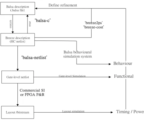
(14) Figure 2: The Balsa Design Flow An overview of the Balsa design flow is shown in figure 2. A Balsa description of a circuit is compiled using balsa-c to an intermediate breeze description. The breeze description is a syntax-directed fashion with language constructs being mapped into networks of parameterized instances of “handshake components”. Each of “handshake components” has a concrete gate level implementation [1] . A number of tools are available to process the breeze handshake files. balsa-netlist automatically generates CAD native netlist files, which can be fed into the commercial CAD tools that further synthesize the netlist to the fabricable layout. Balsa support three commercial CAD systems: Compass Design Automation tools from Avant, Xilinx FPGA design tools and Cadence Design Framework II. Balsa supports three back-end protocols for use with each technology: bundle-data scheme using a four-phase-broad/reduced-broad signaling protocol, a delay-insensitive dual-rail encoding and a delay-insensitive one-of-four encoding. The bundled-data back end should be faster and smaller, but needs more careful post-layout timing validation. The two. 5.
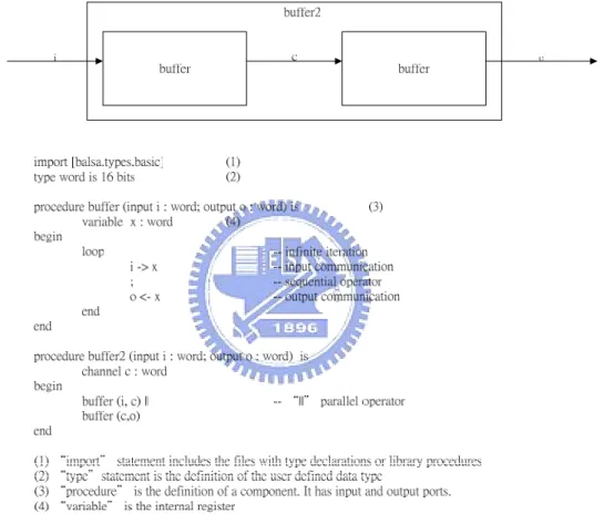
(15) delay-insensitive schemes are larger and slower but should be more robust to layout variations. Balsa supports behavioral simulation by breeze-sim. This simulator allows source level debugging, visualization of the channel activity at the handshake circuit level as well as producing conventional waveform traces that can be viewed using the waveform viewer gtkwave.. Figure 3: Two-place buffer. Figure 3 illustrates a simple Balsa modeling example of a two-place buffer.. 6.
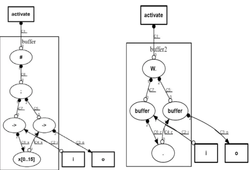
(16) Figure 4: Handshake circuit of a two-place buffer Figure 4 illustrate the handshake component of the two-place buffer generated by breeze2ps. The left hand is a one-place buffer. The right hand is a two-place buffer composed of two one-place buffers.. 1-4 Organization of this thesis In this thesis, we will illustrate the related work in chapter 2 including the overview of the synchronous 8051, classification of asynchronous circuits and the basic cells in Balsa synthesis system. In chapter 3 we will illustrate design of SA8051 modeled by Balsa. In chapter 4 we will illustrate the implementation and verification of SA8051. In chapter 5 we will illustrate the results of simulation. In chapter 6 we will discuss some design issues about Balsa tool, Xilinx synthesis tool and implementation on FPGA. Finally, a brief conclusion and future work are discussed in chapter 7.. 7.
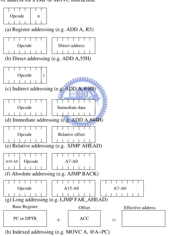
(17) Chapter 2 Related Work This chapter is organized as follows. We first briefly introduce the architecture of the synchronous 8051. We then describe the classification of asynchronous circuits according to the delay assumptions. Finally, we describe several basic cells generated by Balsa synthesis tool.. 2-1 Overview of 8051 In this section we will describe the instruction set and the architecture of the Intel 8051.. 2-1-1 Instruction Set The 8051 is a complex instruction set computer (CISC). It has 255 variable-length instructions from one to three bytes and supports various addressing modes. The opcode of an instruction is always encoded in the first byte. The second and third bytes are operands. The instruction set is divided among five functional groups: arithmetic, logical, data transfer, Boolean variable and program branching. The 8051 is a Harvard architecture: instruction memory and data memory are separate. The instruction set provides eight addressing modes [11] as depicted in figure 4 : (a) in register addressing, instructions are encoded using the three least-significant bits of the instruction opcode (b) in direct addressing, the operand is specified by an 8-bit address field in the instruction representing an address in the internal data RAM or a special-function register (SFR) (c) in indirect addressing, the instruction specifies a register (R0 or R1) containing the address of the operand in data memory (d) in immediate addressing, the constant operand value is part of the instruction (e) in relative addressing, a relative address (or offset) is an 8-bit signed value, which is added to the program counter to form the address of the next instruction executed. (f) in absolute addressing, these instructions allow branching. 8.
(18) within the current 2K page of code memory by providing the 11 least-significant bits of the destination address. (g) in long addressing, these instructions include a full 16-bit destination address as bytes 2 and 3 of the instruction. (h) Indexed addressing uses a base register (either the program counter or the data pointer) and an offset (the accumulator) in forming the effective address for a JMP or MOVC instruction. Opcode. n. (a) Register addressing (e.g. ADD A, R5) Opcode. Direct address. (b) Direct addressing (e.g. ADD A,55H) Opcode. i. (c) Indirect addressing (e.g. ADD A,@R0). Opcode. Immediate data. (d) Immediate addressing (e.g. ADD A,#44H) Opcode. Relative offset. (e) Relative addressing (e.g. SJMP AHEAD) A10-A8. Opcode. A7-A0. (f) Absolute addressing (e.g. AJMP BACK) Opcode. A15-A8. A7-A0. (g) Long addressing (e.g. LJMP FAR_AHEAD) Base Register PC or DPTR. Offset. +. ACC. Effective address. =. (h) Indexed addressing (e.g. MOVC A, @A+PC). Figure 4: The 8051 addressing mode. 9.
(19) H. P0. P1. P2. P3. P4. P5. P6. P7. P8. P9. PA. PB. PC. PD. PE. PF. NOP. JBC. JB. JNB. JC. JNC. JZ. JNZ. SJMP. MOV. ORL. ANL. PUSH. POP. MOVX. MOVX. bit,rel. bit,rel. bit,rel. rel. rel. rel. rel. rel. DPTR,#. C,/bit. C,/bit. dir. dir. A,. @DPTR,. @DPTR. A. L R0. dara 16 R1. AJMP. ACALL. AJMP. ACALL. AJMP. ACALL. AJMP. ACALL. AJMP. ACALL. AJMP. ACALL. AJMP. ACALL. AJMP. ACALL. R2. LJMP. LCALL. RET. RETI. ORL. ANL. XRL. ORL. ANL. MOV. MOV. CPL. CLR. SETB. MOVX. MOVX. addr16. addr16. dir,A. dir,A. dir,A. C,bit. C,bit. bit,C. C,bit. bit. bit. bit. A,@R0. @R0,A. RR. RRC. RL. RLC. ORL. ANL. XRL. JMP. MOVC. MOVC. INC. CPL. CLR. SET. MOVX. MOVX. A. A. A. A. dir,#data. dir,#data. dir,#data. @A+DPTR. A,@A+PC. A,@A+DPTR. DPTR. C. C. C. A,@R1. @R1,A. INC. DEC. ADD. ADDC. ORL. ANL. XRL. MOV. DIV. SUBB. MUL. CJNE A,. SWAP. DA. CLR. CPL. A. A. A,#data. A,#data. A,#data. A,#data. A,#data. A,#data. AB. A,#data. AB. #data,. A. A. A. A. R3. R4. rel R5. R67. INC. DEC. ADD. ADDC. ORL. ANL. XRL. MOV. MOV. SUBB. CJNE A,. XCH. DJNZ. MOV. MOV. dir. dir. A,dir. A,dir. A,dir. A,dir. A,dir. dir,#data. dir,dir. A,dir. dir,rel. A,dir. dir,rel. A,dir. dir,A. INC. DEC. ADD. ADDC. ORL. ANL. XRL. MOV. MOV. SUBB. MOV. CJNE. XCH. XCHD. MOV. MOV. @Ri. @Ri. A,@Ri. A,@Ri. A,@Ri. A,@Ri. A,@Ri. @Ri,#data. dir,@Ri. A,@Ri. @Ri,dir. @Ri. A,@Ri. A,@Ri. A,@Ri. @Ri,A. ,#data ,rel R8F. INC. DEC. ADD. ADDC. ORL. ANL. XRL. MOV. MOV. SUBB. MOV. CJNE. XCH. DJNZ. MOV. MOV. Rn. Rn. A,Rn. A,Rn. A,Rn. A,Rn. A,Rn. Rn,#data. dir,Rn. A,Rn. Rn,dir. Rn. A,Rn. Rn,rel. A,Rn. Rn,A. ,#data ,rel. Table 2: The 8051 instruction set. All mnemonics copyrighted Intel Corporation 1980 10.
(20) Table 2 is the complete instruction set of 8051. In this table the rows represent the four least significant bits of the opcode while the columns represent the four most significant bits. Thus, the instruction at entry PiRj has opcode ij in hexadecimal notation. Rows R8 to RF are combined into one row because these instructions only differ in the last three bits which specify a register. Rows R6 and R7 are also combined into one row because the last bit of opcode indicates which register (R0 or R1) will be used as indirect address. Note that only one entry (PA R5) in this table does not contain an instruction.. 2-1-2 Synchronous Architecture. Figure 5: The architecture of the synchronous 8051 11.
(21) Figure 5 is the architecture of the synchronous 8051 [12]. It has three buses: IB, PB, PARB bus. IB-bus acts as the communication channel between any two registers. PB-bus acts the communication channel among PAR (Program Address Register), Buffer, PC Incrementer, PC and DPTR. PAR sent out program address on PAR-bus. The width of the IB bus is 1 byte while the PARB and PB are 2 bytes. The internal memory consists of on-chip ROM and on-chip data RAM. The on-chip RAM contains a rich arrangement of general-purpose storage, bit-addressable storage, register banks, and special function registers (SFR). The registers and input/output ports are memory mapped and accessible like any other memory location and the stack resides within the internal RAM rather than in external RAM. SFRs take care of the communication between CPU and peripherals. There are four bidirectional ports (P0 – P3) for communication to and from the outside world. The 8051 also includes bit operations, which only affect single bit in a given registers. Only some locations of the internal RAM are bit-accessible including address from 20H to 2FH and some SFRs. Internally, the bit operations are performed by reading the whole byte from internal memory, modifying the single bit, and then writing the value back in the same operation cycle. Table 3 is the instruction scheme of the synchronous 8051 [13]. Each instruction is executed in one, two or four machine cycles. A machine cycle consists of a sequence of 6 states, numbered S1 through S6. Each state time lasts for two oscillator periods. Therefore, with an internal clock frequency of 12 MHz the performance will be below 1 MIPS. In each state of the execution scheme a specific action takes place. The one-cycle instructions execute the first machine cycle C1, while the two-cycle instructions execute C1 and C2 consecutively. The scheme results in many redundant cycles during execution because not all actions are required in one machine cycle. For example, two program fetches are generated during each machine cycle, even if the instruction being executed does not require it. 12.
(22) C1. S1. S2. S3. S4. S5. S6. Access. ACC -> T2. Access. Access. OP->T1 or T2. ALU->dest.. RAM. ROM. S3. S4. S5. S6. PC incr.. OP->T1 or T2. ALU->dest.. ROM. C2. S1. S2. Access. Calculate jump address. ROM Table 3: Instruction execution scheme When access for external memory, Port 0 has the data byte and the least significant byte of the address multiplexed on it. Address Latch Enable (ALE) is used to signal external circuitry to latch the address LSB before Port 0 switches to either reading or writing the data byte. If a 16-bit address is used, Port 2 is used to output the high byte of the address. In this mode, Port 2 also uses strong internal pull-ups to output the address MSB. Finally, pins 6 and 7 of Port 3 are used to signal a write or a read on the bus respectively. However, for the SA8051, all of the instructions are in internal memory.. 2-2 Classification of Asynchronous Circuits. Figure 6: A circuit fragment with gate and wire delays At the gate level, asynchronous circuits can be classified as being delay-insensitive, quasi-delay-insensitive, speed-independent, self-timed depending on the delay assumptions that are made [4]. Figure 6 serves to illustrate the following discussion. In this figure there are three gates (A, B, C) and three wires (W1, W2, W3). dA, dB and dC represent the gate delay for A, B and C respectively. d1, d2 and d3 represent the wire delay of W1, W2 and W3 respectively. 13.
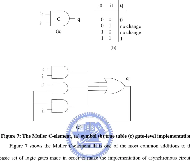
(23) (a) Delay-Insensitive (DI): a circuit that operates correctly with positive, bounded but unknown delays in wires and gates. Referring to figure 6 this means arbitrary dA, dB, dC, d1, d2 and d3. (b) Quasi-Delay-Insensitive (QDI): a QDI circuit is DI with the exception of some carefully identified wire forks called “isochronic forks”. Referring to figure 6 this means arbitrary dA, dB, dC, d1 but d2 = d3. (c) Speed-Independent (SI): a SI circuit is a circuit that operates correctly assuming positive, bounded but unknown delays in gates and ideal zero-delay wires. Referring to figure 6 this means arbitrary dA, dB, dC but d1 = d2 = d3 = 0. (d) Self-Timed (ST): a self-timed circuit contains a group of self-timed elements. Each element is contained in an “equipotential region”, where wires have negligible or well-bounded delay. An element itself may be an SI circuit, or a circuit whose correct operation relies on use of local timing assumptions. However, no timing assumptions are made on the communication between regions. That is, communication between regions is DI.. 2-3 Balsa Back-End The Balsa back-end generates gate level netlist to import into target CAD systems in order to produce circuit implementations [14]. In this section we will describe some basic cells for Xilinx technology generated by Balsa such as Muller C element and S element. We also describe some handshake components in Balsa synthesis system.. 2-3-1 Basic Elements The gate level netlist generated by Balsa for Xilinx technology only uses some basic cells including AND, OR, NOR, XOR, NADN, BUF, XNOR, INV, FD (D-type flip-flop), 14.
(24) FDC and FDCE. Basic elements are composed of these cells. i0. i1. q. 0 1 0 1. 0 no change no change 1. i0 i1. C. q. 0 0 1 1. (a). (b). i0 i1. q. i0. i1 (c) Figure 7: The Muller C-element, (a) symbol (b) true table (c) gate-level implementation Figure 7 shows the Muller C-element. It is one of the most common additions to the basic set of logic gates made in order to make the implementation of asynchronous circuits easier. It is a state-holding element like an asynchronous set-reset latch. When both inputs are 0, the output is set to 0. When both inputs are 1 the output is set to 1. For other input combinations the output does not change. A Muller C-element is a fundamental component that is extensively used in asynchronous circuits.. 15.
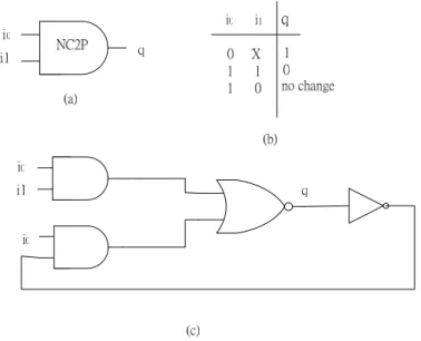
(25) Figure 8: The NC2P-element (a) symbol (b) true table (c) gate-level implementation Figure 8 shows the NC2P element. When i0 is equal to 0, the output is 0. When i0 and i1 are equal to 1, the output is 1. For other input combinations the output does not change. It is much like inverter of C-element except that when i0 is equal to 0 and i1 is equal to 1, the output is 1.. Figure 9: The S-element (a) symbol (b) gate-level implementation (c) handshaking protocol Figure 9 shows the S-element which is a circuit element commonly found in the implementation of handshake components [1]. An S-element has 4 pins including 2 request/acknowledge handshake pairs – ‘Ar’/’Aa’ and ‘Br’/’Ba’. In Balsa system it replaces 16.
(26) the “inverter of C-element” with “nc2p”. Hence, it can reduce the number of gates because “inverter of C-element” uses 3 AND gates, 1 OR gate and 1 Inverter but “nc2p” uses 2 AND gates, 1 NOR gate and 1 Inverter.. Figure 10: The multiplexer (a) function block (b) true table (c) gate level implementation. Figure 11: The de-multiplexer (a) function block (b) true table (c) gate level implementation Figure 10 and figure 11 are the multiplexer and de-multiplexer elements. They are used in many elements such as Basla full adder and BrzCase.. 2-3-2 Handshake Components Balsa has about 40 components that use handshake signaling for communication. Each of “handshake components” has a concrete gate level implementation. In the following we 17.
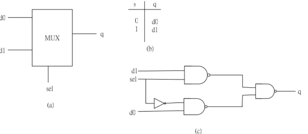
(27) illustrate some handshake components [14] .. Figure 12: The Fetch Component (a) handshake component (b) gate level implementation Figure 12 is the Fetch component. This component is the most common way of controlling a datapath from a control tree. Transferrers are used to implement assignment, input and output channel operations in Balsa by transferring a data value from a pull datapath and pushing it towards a push datapath [14].. Figure 13: The Sequence Component (a) handshake component (b) gate level implementation. Figure 14 and 15 are sequence and concurrent component respectively. They form a large part of handshake circuit control trees [14]. They are used to activate a number of commands under the control of activate handshake.. 18.
(28) Figure 14: The Concurrent Component (a) handshake component (b) gate level implementation. Read[0]. write Var. (a) Read[1]. (b). Figure 15: The Variable Component (a) handshake component (b) gate level implementation Figure 15 is the variable component. It uses D-type flip-flop to store data. The source of clock is the signal write_0r. When a piece of data is wanted to be stored, the signal write_0r is set and then the signal is reset. When a piece of data is wanted to be read, the signal read_0r or read_1r is set. It is natural to achieve the effect of gating clock.. 19.
(29) 2-4 Concluding Remarks In this chapter we introduce the synchronous 8051 architecture. 8051 is a complex instruction set computer. It has variable-length instructions from one to three bytes. Each state of a machine cycle uses the bus. Hence, it is not easy to overlap execution of instructions, i.e. to implement pipelining. We then introduce the classification of the asynchronous circuits. Asynchronous circuits can be classified as being SI, DI, QDI, ST depending on the delay assumptions. Finally we illustrate the Balsa back-end. Balsa synthesis system is composed of about 40 components. Each can be translated to gate level netlist. They use handshaking protocol for communication.. 20.
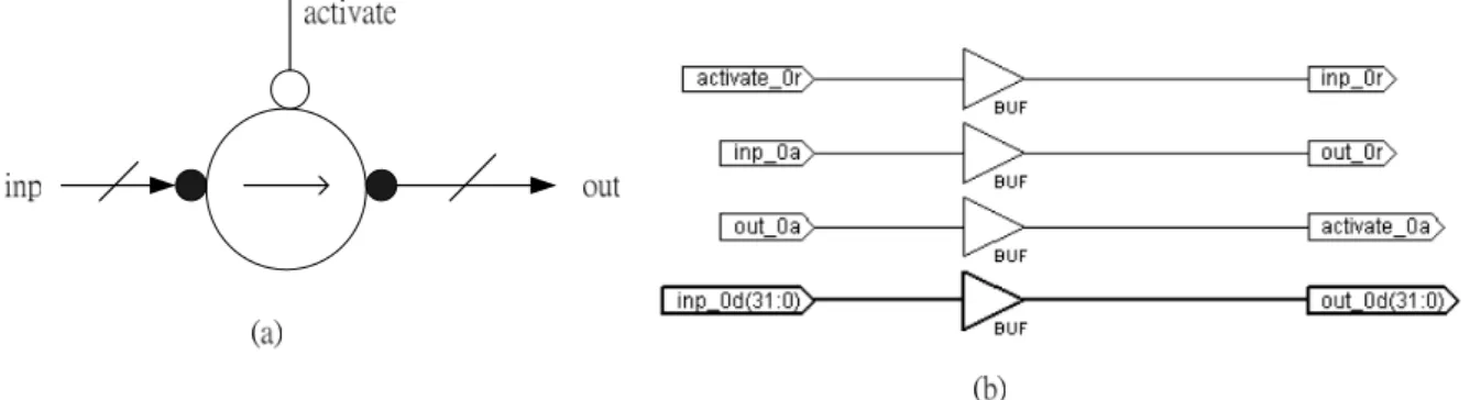
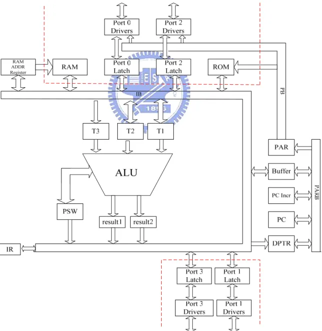
(30) Chapter 3 Design the SA8051 This chapter is organized as follows. First, we describe the architecture of SA8051 and model it in Balsa. We then describe the interface among the CPU, memory and external environment. We then discuss the optimization in control path. Finally, we describe the technique of bypassing the buses and ALU.. 3-1 The Architecture of SA8051 activate_0r. reset_0a reset_0r. rom_en rom_addr. rom__addr_0r rom__addr_0a rom_addr_0d. rom_data. rom__data_0r rom__data_0a. Rom_rfd. rom_data_0d. P0_out P1_out P2_out P3_out. handshake interface. 5 MHz. P0_in P1_in P2_in P3_in. Figure 16: The architecture of SA8051 21. reset_0d.
(31) The global structure of the SA8051 consists of CPU, ROM, RAM, four inputs and four outputs as depicted in figure 16. The CPU is activated when the signalactivate_0r is set to 1. If the CPU is not activated, it is in idle mode and consumes little energy. The CPU communicates with RAM and ROM through handshaking interface. It has four output ports including P0_out, P1_out, P2_out and P3_out. Each has one byte and is mapped to one location of RAM. It has four input ports including P0_in, P1_in, P2_in and P3_in. They are used to receive data from the environment. When we set the signal reset_0d, the CPU will initialize the contents of all special function registers (SFRs).. Figure 17: The architecture of CPU 22.
(32) Figure 17 depicts the architecture of the CPU in SA8051. It is a little different from synchronous architecture. The ALU (Arithmetic and Logic Unit) has three inputs (T1, T2 and T3), two outputs (result1 and result2) and a PSW (Program Status Word). Most instructions only use two inputs (T1 and T2) and one output (result1). Few instructions use three inputs and two outputs such as MUL, DIV and JMP. But some instructions do not use ALU such as MOV. It can reduce power consumption and promote performance but need extra cost. The registers T1, T2 and RAR (RAM Address Register) have an input and an output port in order to support some instructions with bypassing technique. We will describe this technique in the following section. The broken lines in this figure separate the processor core and the peripheral of SA8051.. Figure 18: Balsa program for main loop of CPU The main loop of the Balsa program for the CPU takes the form as shown is figure 18. Initially, SA8051 resets the contents of each SFR (Special Function Register) and PC (Program Counter). In the loop, prior to executing an instruction there has to be a check to see the reset has occurred. Then, fetch the first byte of the instruction and increment the PC. The opcode is in the first byte of each instruction. Finally, the execution unit decodes the opcode and executes the corresponding operations.. 23.
(33) 3-2 Design the Fetch_ir Unit Fetching an instruction involves sending an address to the program memory, receiving the corresponding instruction opcode and incrementing the program counter as shown in figure 19. par_b and p_b mean PAR bus and PB bus respectively as shown in figure 17. First, pc assigns its value to par_b and par receives value from par_b. Then, par assigns its value to p_b and p_b is sent out by the channel of rom_addr. Finally, the bus receives data from the channel of rom_data and assigns its value to ir (instruction register).. Figure 19: Balsa program for Fetch_ir. 3-3 Design the ALU Figure 20 shows the block diagram of the ALU in Balsa. The ALU has six input ports and five output ports. We describe the meaning of these ports in table 4 in detail. The port alu_op decides which operation the ALU will do. The two input flags src_cy and src_ac are bit 6 and bit 7 respectively inside PSW. The ALU has three data input ports including src_1, src_2 and src_3. Most instructions only use src_1 and src_2. Some instructions use src_3 like MOVC and CJNE. There are two data output ports in ALU including result_1 and result_2. Most instructions only use result_1 but some instructions like MOVC and CJNE use result_1 and result_2. Some operations will update the flags like ADD and SUB.. 24.
(34) Figure 20: The block diagram of ALU I/O Port. Port Type. Port Size. Description. alu_op. in. 5 bits. ALU Operation Code. src_1. in. 8 bits. ALU input data. src_2. in. 8 bits. ALU input data. src_3. in. 8 bits. ALU input data. src_cy. in. 1 bit. Carry flag. src_ac. In. 1 bit. Auxiliary Carry Flag. result_1. out. 8 bits. ALU Result1. result_2. out. 8 bits. ALU Result2. result_cy. out. 1 bit. Carry flag. result_ac. out. 1 bit. Auxiliary Carry flag. result_ov. out. 1 bit. Overflow flag. Table 4: The description of the ports in ALU Balsa adopts the method of syntax-directed compilation. The transparent compilation of a Balsa program into an asynchronous circuit implies that for each expression in the Balsa text a separate piece of hardware is generated. We can reduce area by sharing some pieces of hardware. For example, we combine the function of ADD and SUB. We use shared procedure to implement it in Balsa Figure 21 is an example for combing these functions of ADD and SUB. The shared 25.
(35) procedure does add src_1, src_2 and ci or subtract src_2 and ci from src_1. If the shared function does SUB, it adds src_1, inverter of the src_2 and inverter of the src_cy. The shared function also updates the flags: carry, auxiliary and overflow flag. Similar shared functions can be programmed for the bit-wise Boolean operations AND, OR and XOR.. Figure 21: (a) Balsa shared function for ADD and SUB (b) operands assignment used in AddSub function.. 3-3 Design the Decoder Unit After fetching the first byte of the instruction, the CPU decodes the instruction opcode in register ir, and executes the statements associated with that instruction. If we observe the 8051 26.
(36) instruction set in table 4, we can find the partial regularity of the instruction set. We can take this advantage to decode an instruction in order to reduce area cost. For example, in row R8 to RF each column has the same instruction only differing in the index of the operand Rn. Similar arguments go for rows 6 and 7. In this table, the regular part is gray and irregularity increases when going to the above. So, we can decode the instruction set in rows (least four significant bits) first and decode in columns (most four significant bits) to determine the instruction to execute.. 27.
(37) H. P0. P1. P2. P3. P4. P5. P6. P7. P8. P9. PA. PB. PC. PD. PE. PF. NOP. JBC. JB. JNB. JC. JNC. JZ. JNZ. SJMP. MOV. ORL. ANL. PUSH. POP. MOVX. MOVX. bit,rel. bit,rel. bit,rel. rel. rel. rel. rel. rel. DPTR,#. C,/bit. C,/bit. dir. dir. A,. @DPTR,. @DPTR. A. L R0. dara 16 R1. AJMP. ACALL. AJMP. ACALL. AJMP. ACALL. AJMP. ACALL. AJMP. ACALL. AJMP. ACALL. AJMP. ACALL. AJMP. ACALL. R2. LJMP. LCALL. RET. RETI. ORL. ANL. XRL. ORL. ANL. MOV. MOV. CPL. CLR. SETB. MOVX. MOVX. addr16. addr16. dir,A. dir,A. dir,A. C,bit. C,bit. bit,C. C,bit. bit. bit. bit. A,@R0. @R0,A. RR. RRC. RL. RLC. ORL. ANL. XRL. JMP. MOVC. MOVC. INC. CPL. CLR. SET. MOVX. MOVX. A. A. A. A. dir,#data. dir,#data. dir,#data. @A+DPTR. A,@A+PC. A,@A+DPTR. DPTR. C. C. C. A,@R1. @R1,A. INC. DEC. ADD. ADDC. ORL. ANL. XRL. MOV. DIV. SUBB. MUL. CJNE A,. SWAP. DA. CLR. CPL. A. A. A,#data. A,#data. A,#data. A,#data. A,#data. A,#data. AB. A,#data. AB. #data,. A. A. A. A. R3. R4. rel R5. R67. INC. DEC. ADD. ADDC. ORL. ANL. XRL. MOV. MOV. SUBB. CJNE A,. XCH. DJNZ. MOV. MOV. dir. dir. A,dir. A,dir. A,dir. A,dir. A,dir. dir,#data. dir,dir. A,dir. dir,rel. A,dir. dir,rel. A,dir. dir,A. INC. DEC. ADD. ADDC. ORL. ANL. XRL. MOV. MOV. SUBB. MOV. CJNE. XCH. XCHD. MOV. MOV. @Ri. @Ri. A,@Ri. A,@Ri. A,@Ri. A,@Ri. A,@Ri. @Ri,#data. dir,@Ri. A,@Ri. @Ri,dir. @Ri. A,@Ri. A,@Ri. A,@Ri. @Ri,A. #data ,rel R8F. INC. DEC. ADD. ADDC. ORL. ANL. XRL. MOV. MOV. SUBB. MOV. CJNE. XCH. DJNZ. MOV. MOV. Rn. Rn. A,Rn. A,Rn. A,Rn. A,Rn. A,Rn. Rn,#data. dir,Rn. A,Rn. Rn,dir. Rn. A,Rn. Rn,rel. A,Rn. Rn,A. #data ,rel. Table 5: Regular (gray part) and Irregular (white part) part of the 8051 instruction set 28.
(38) We need a decoder to judge whether the instruction opcode belongs to the regular or irregular part. The shared function judge_regular is described in figure 22. The L_ir is the least four significant bits of the instruction register and H_ir is the most four significant bits of the instruction register. If the instruction belongs to regular part, the register regular is set.. Figure 22: The judge_regular shared function. Most instructions in the regular part have the same characteristic as shown in figure 23. They get its first operand from ROM or RAM and store it in the register T1. Then, they may get the second operand from RAM and store it in the register T2. Finally, they execute the corresponding operation and store the result in the destination register.. Figure 23: The structure of the regular part. 29.
(39) 3-4 Deal with Bit-Operation Instructions The 8051 contains 210 bit-addressable locations, of which 128 are at byte addresses 20H through 2FH, and the rest are in the special function registers. The instructions using bit-addressing mode can be classified into two kinds as shown in table 5. First, those instructions fetch a bit from the data memory and don’t modify it. Second, those instructions fetch a bit from data memory, modify it and write it back.. First kind. Second kind. MNEMONIC. DESCRIPTION. JC rel. Jump if Carry set. JB bit, rel. Jump if bit set. JBC bit, rel. Jump if bit set and clear bit. JNB bit, rel. Jump if bit not set. JNC rel. Jump if Carry not set. MOV C, bit. Move bit variable. ANL C, <src-bit>. ANL bit with C, ANL NOT bit with C. CLR bit. Clear bit. CPL bit. Complement bit. ORL C, <src-bit>. OR bit with C , OR NOT bit with C. Table 6: Instructions with bit-addressing mode When a bit-addressable instruction is executed, the byte data containing this bit will be fetched from the data memory. We store this byte in register T1 and need a register bit_index to record which bit we want to read or modify. If an instruction wants to modify this bit, it will modify it in register T1 indexed by the register bit_index. Figure 24 depicts the Balsa program for dealing with bit-addressable instruction.. 30.
(40) Figure 24: (a) Set the value of the rar and bit_data_index (b) Get byte from the data memory and store it in register T1. 3-5 Handshake Interface to the Memory We add a handshake interface between the memory and the CPU due to the synchronous RAM and ROM. When the CPU wants to fetch an instruction from the ROM, it sets the both signals rom_addr_0r and rom_data_0r and sends out the address. A C-element is employed in order to check if rom_addr_0r and rom_data_0r are both set or reset. When the both are set, the ROM is enabled and after the latency 6 ns the Rom_rfd is set. After delaying about a clock cycle, the signals rom_addr_0a and rom_data_0a are set. The following is the return-to-zero portion of the handshake protocol. In order to make it quick, we employ an asynchronous CLR input in a D-type flip flop. The acknowledge signals of the CPU can be reset quickly when the signal Rom_rfd is reset. The handshake interface between the CPU and the RAM is a little different from the ROM. If the CPU wants to read data from RAM, it set the signal ram_in_data_0r. If the CPU wants to store data in RAM, it set the signal ram_out_data_0r. So, an OR gate is employed to connect the both signals. The data is wrote or read according to the signal Ram_rNw_0d when. 31.
(41) the signal Ram_en is set. After the latency 6 ns, the Ram_rfd is set and delaying about a clock cycle the acknowledge signals are set. The worst case of memory access is delaying about 2 clock cycles due to the handshake interface. Hence, it is important to reduce the number of times of fetching the data from the ROM or RAM. For example, in the synchronous 8051 the machine cycle 1 of the execution scheme read data from the ROM two times. Not all instructions need to fetch two pieces of data from the ROM. We avoid this situation in the SA8051 in order to increase the performance. This can also reduce the energy dissipation for the memory.. Figure 25: Handshake interface between Memory and CPU 32.
(42) 3-6 Bypassing the Bus and ALU There are three buses: I-Bus, P-Bus and PAR-Bus in the 8051 as shown in figure 17. It is possible to mimic the synchronous bus implementation by introducing the variables IB, PB and PARB in the Balsa syntax. Each communication between any two registers is finished by using the buses. The source register is copied to the bus first and then the destination register receives data from the bus. For example, if the content of the register PC wants to be copied to the register PAR, we write PBus := PC ; PAR := PBus If we use the bus bypassing technique, the above statements can be rewritten as PAR := PC This can reduce the area cost due to the deleted sequencer component (;). But it introduces multiplexers (BreezeCall component) in the front of the destination register when more than one assignment to the register is happened. If the bus bypassing technique is not introduced, there is only one multiplexer on the writeport of the variable PBus and the PAR does not need a multiplexer. The less the number of times of data is accessed, the more energy is saved. So, it can save energy dissipation by introducing the bus bypassing technique on the frequently used communication paths. The table 6 shows the opportunities for bypassing the bus among the registers.. Source Register. Destination Register. The bypassing bus. PC (Program Counter). PAR (Program Address. PARB. Register) Result1 @ Result2 (ALU results). Buffer. IB. T1. RAR (RAM Address. IB. Register). 33.
(43) T1. T2. IB. T2. RAR. IB. Table 7: The opportunity for bypassing the bus In the 8051 not all instructions need the arithmetic or logic operations. In other words, some instructions don’t transfer the data to the ALU and wait for the operation completed in order to speed up and save energy dissipation. For example, the instruction MOV just moves the data between the registers and need not any arithmetic or logical operations. So, it does not do the ALU operations. In the asynchronous architecture we can achieve the bypassing ALU technique naturally.. 3-7 Optimizations in Control Path As the previous descriptions in section 3-2 the transparent compilation of a Balsa program into an asynchronous circuit implies that for each statement in the Balsa text a separate piece of hardware is generated. We can optimize the control path in the Balsa text. For example, the 8051 CPU contains the following fragment of the program. The signal isel is a bit data for selection. Each of these four statements (S0, S1, P0, P1) represents a piece of hardware. The corresponding handshake circuit generated by Balsa is shown in figure 26 (a).. 34.
(44) Figure 26: handshake circuit for the case-statement (a) not optimized (b) optimized The case-statement can be rewritten as. The corresponding handshake circuit generated by Balsa is shown in figure 26 (b). We can compare the two handshake circuits. In figure 26 (a) there are a case (labeled “@”), two sequencer (labeled “;”) and two call (labeled “|”) components. On the other hand, in figure 26 (b) there are only a sequencer and a case component. It is better in terms of area, speed and power than the circuit in figure 26 (a).. 35.
(45) 3-8 Concluding Remarks In this chapter we illustrate the architecture of the asynchronous 8051 and model it in Balsa language. We describe some techniques for optimizing the ALU and the decoder unit in the SA8051. We then describe the method to deal with bit-operation instructions. The handshake interface is design due to communicating with synchronous memory. The bypassing techniques are also introduced in order to reduce the power and area cost. Finally, we describe some optimizations in control path due to the syntax-direct compilation in Balsa.. 36.
(46) Chapter 4 Implementation and Verification This chapter is organized as follows. First, we illustrate a design flow for asynchronous implementation on a synchronous FPGA. Then we describe some implementation issues. Finally, we illustrate the verification methods.. 4-1 The Design Flow The asynchronous 8051 core is modeled by Balsa language. Descriptions of the 8051 core (.balsa file) are then translated (balsa-c) into implementations in a syntax directed-fashion with language constructs being mapped into networks of parameterized instances of “handshake components” (.breeze file) each of which has a concrete gate level implementation. balsa-netlist automatically generates Verilog netlist for Xilinx synthesis tool. The following steps are design flow for FPGA. The Verilog netlist generated by balsa-netlist is converted into a netlist of basic gates in the synthesis step of the design flow. The netlist may be optimized using technology-independent logic minimization algorithms. However, we must avoid the logic minimization for hazard free circuits and buffers generated by balsa-netlist. We add the constraint “keep hierarchy” to avoid the logic minimization. Then the synthesized netlist is mapped to the target device using a technology-mapping algorithm. The placement algorithm maps logic blocks from the netlist to physical locations on an FPGA. On the placement has been done, the routing algorithm determines how to interconnect the logic blocks using the available routing. The final output of the design flow is the FPGA programming file, which is a bit stream determining the state of every programmable element inside an FPGA. The design flow is shown is figure 27.. 37.
(47) Figure 27: The Balsa and FPGA design flow. 38.
(48) 4-2 Implementation Issues Compilation from Balsa programs to Xilinx netlist proceeds in two steps. In first step, handshake circuits form the intermediate architectures. An important characteristic about this compilation is that it is transparent, which allows feedback about important performance characteristics such as performance, area, timing and testability to be generated at the handshake circuit level and to be presented to the VLSI programmer at the Balsa level. When the designer is satisfied with the performance of the Balsa program, the corresponding handshake circuit is expanded into a gate-level netlist. At this level the design can be simulated to obtain more accurate performance figures using commercial simulators. We choose four-phase bundled data protocol to implement the handshake circuit instead of dual-rail encoding in order to reduce the area cost. Handshake circuits are implemented only using standard cells such as AND, OR, Inverter gate and flip flop. We must pay attention to delay matching and the verification (after routing) of the timing assumptions that have been made. In order to minimize the verification effort, delay-matching is conserved. We add enough buffers on the all request signals on the push channel and the acknowledge signals on the pull channel. Because there are no asynchronous cells in FPGA, all handshake circuits are mapped onto standard cells. This results in the area overhead of the handshake circuits. It is to be noted that the Xilinx synthesis tool could do logic minimization but it must be avoided. There are hazard-free circuits and buffers in asynchronous circuits. They can not be minimized. We can avoid this situation by adding the constraint “keep hierarchy” on the handshake modules. RAM and ROM are not modeled by Balsa language. We implement them using the block RAM on FPGA in order to reduce area cost. We add a handshake interface between the 8051 core and the memory. The signal rfd is employed in the RAM and ROM to provide. 39.
(49) completion detection of reading or writing operations. Until now all instructions can be executed except MUL, DIV and MOVX. The peripherals are not considered such as timers and UART. The design was realized in Xilinx FPGA SPARTAN IIE 300 ft256.. 4-3 Verification In this section we illustrate the verification for the SA8051. There are three steps for verification. First, we do behaviour simulation in Balsa environment. Then, we do timing simulation in Xilinx environment. In this step we must check the timing validity on control circuits. Finally, we do verification on FPGA board.. 4-3-1 Behavior Simulation The environment used to do behavior simulation for SA8051 is illustrated in figure 28. The memory model ROM and RAM are the two predefined procedures in Balas as shown in figure 29. We assign the address width and data width to determine their size. The ROM size is 4K bytes and the RAM size is 256 bytes. The contents of the ROM are loaded during initialization as 8-bit quantities in the hexadecimal format from a hexadecimal file. A hexadecimal file is translated from a C program by KEIL tool [15]. Whenever an addressing arrives at the ROM model from the ROM address channel, the ROM outputs the instruction code. When the processor wants to write data, it sets the signal rNw and sends out the address and the data. When the processor wants to read data from RAM, it resets the signal rNw and sends the address and the data. The 8051 simulator executes the instructions in the hexadecimal file. The execution results are compared with the contents of the RAM. If the results are not equal, we must modify the code of the processor. 40.
(50) SA8051 (Balsa). No. =. RAM Model (Balsa). ROM Model (Balsa). Yes. Correct. Execution Result. 8051 Simulator. 8051 HEX file KEIL-oh51. 8051 Object Code KEIL-c51 KEIL-a51 KEIL-bl51. Source file (C). Figure 28: SA8051 behavior simulation environment. Figure 29: Balsa description for memory model (a) ROM model (b) RAM model. 41.
(51) 4-3-2 Timing Simulation When completing the behavior simulation in Balsa environment, the following step is to do timing simulation as shown in figure 30. The ROM model is automatically generated from a hexadecimal file by Xilinx CORE generator [16]. The RAM model is also generated by it. The memory model implemented by block RAM on FPGA is combined with the processor core netlist synthesized by balsa-netlist through handshake interface. Before synthesizing, the constraint file must be added. The content of the constraint file is the “keep hierarchy” constraint on some handshake modules. The constraint file is employed in order to satisfy timing constraints and avoid the logic minimization. When the constraint is added, the synthesis, map, placement and routing are preceded in order. A NCD file is generated after PAR (place & route). The NCD file may contain placement and routing information in varying degrees of completion. NetGen generates netlist that are compatible with Xilinx supported simulation such as ModelSim. The result of timing simulation is compared with the result of the 8051 simulator. If the results are not equal, we must modify the processor netlist generated by balsa-netlist. For example, when the timing violation occurs on flip-flops in BrzVariable modules, we trace the write request signal and find out the corresponding write acknowledge signal. Then we add some buffers ahead of the write acknowledge signal.. 42.
(52) SA8051 Source file (C). CPU Core Netlist (Xilinx). KEIL-c51 KEIL-a51 KEIL-bl51 KEIL-oh51. RAM Model (EDIF). 8051 Simulator. 8051 HEX. ROM Model (EDIF). Constraint File. Result. Synthesis No. =. MAP. Placement and Routing. Yes. Correct. Result. NetGen. Timing Simulation. Figure 30: SA8051 timing simulation environment. 4-3-3 Board Level Verification After timing simulation, we do verification on Digilent D2-FT system board [17] with the device Xilinx FPGA SPARTAN IIE 300 ft256. There is a frequency divider circuit on the top module because of the 50 MHz clock on board. The two input ports Activate_0r and reset are connected to the Switch 1 and Switch 2 respectively. The signal reset is set when the frequency divider is enabled. If the signal Activate_0r is set, the CPU is activated. There are 4 output ports connected to 4 seven segments and 16 LEDs respectively in order to display the results. The board level verification environment is shown in figure 31. 43.
(53) 50 MHz. Clock Top P2[7:0]. Activate_0r. reset. CPU Core. RAM. 16-LEDs P1[7:4]. SW 2. P3[7:0]. ROM. P1[3:0]. P0[7:4]. P0[3:0]. SW 1. 7-seg. 7-seg. 7-seg. 7-seg. Figure 31: Board level verification environment. 4-4 Concluding Remarks In this chapter we introduce the design flow for asynchronous circuit implementation in FPGA. Some implementation issues are described. We illustrate the flow of verification including the behavior, timing and board level.. 44.
(54) Chapter 5 Simulation Result This chapter is organized as follows. First, we compare the performance of SA8051 with the Intel 8051 under various clock rates. Then, we compare the power consumption of SA8051 with the synchronous 8051. Finally, we compare the area cost with the synchronous version.. 5-1 Performance The performance of the SA8051 is compared with the Intel 8051, called I8051 developed by University of California [18]. The I8051 models the actual Intel implementation rather closely, e.g., it is 100% instruction compatible. It is written in synthesizable VHDL (at least by Synopsys and Xilinx). We modify it a little in order to compare the SA8051 with it fairly. Hence, we remove the MUL, DIV and MOVX operations from it. The FPGA device Xilinx Spartan IIE 300 ft256 is chosen to estimate the performance. We do timing simulation by ModelSim. We run 6 test programs under different clock rates. There is a clock in the interface between the SA8051 and the memory. Figure 32 shows the speedup of SA8051 versus I8051. The SpeedUp is defined as SpeedUp = Execution Time of I8051 / Execution Time of SA8051 The maximum rate of I8051 is 12 MHz. The performance depends on the clock rate and the tested programs. In sort.c program the SA8051 runs faster than I8051 when the clock rate is less than 8 MHz. In other five programs the SA8051 runs faster than I8051 when the clock rate is less than 6 MHz. When the clock rate is above 8 MHz, the SpeedUp is below 1 for these 6 tested programs. The bottleneck is the interface between the asynchronous processor and the synchronous memory. The worst case for fetching data from memory is 2 clock cycle delays. The same. 45.
(55) situation occurs in writing data. Sort.c Program 1.8. Cast.c Program. 1.68. 1.6. 1.55. 1.6 1.4. 1.02. 1. 0.84. S p eed U p. S p eed U p. 1.31. 1.2. 1.14. 1.2. 1.44. 1.4. 0.79. 0.8 0.6. 0.99. 1. 0.87 0.71. 0.8. 0.4. 0.4. 0.2. 0.2. 0. 0. 2. 4. 6. 8. 10. 12. 2. 4. 6. 8. Fibonacci.c Program. 0.90 0.74. 0.8. S peed U p. S p eedU p. 1.2. 1.02 0.69. 0.6. 1.01. 1. 0.88 0.74. 0.8. 0.65. 0.6. 0.4. 0.4. 0.2. 0.2 0. 0 2. 4. 6. 8. 10. 2. 12. 8. GCD.c Program. Negcnt.c Program 1.8 1.6. 1.38. 1.2. 6 MHz. 1.54. 1.4. 4. MHz. 1.8. 10. 12. 1.57 1.40. 1.4 1.2. 1.04. SpeedUp. SpeedUp. 1.35. 1.4. 1. 1.6. 1.52. 1.6. 1.37. 1.2. 12. int2bin.c Program. 1.48. 1.4. 10. MHz. MHz. 1.6. 0.66. 0.6. 0.90. 1. 0.75. 0.8. 0.67. 1.06 0.91. 1. 0.75. 0.8. 0.68. 0.6. 0.6. 0.4. 0.4. 0.2. 0.2. 0. 0. 2 2. 4. 6. 8. 10. 4. 12. 6. 8 MHz. MHz. Figure 32: SpeedUp for SA8051 versus I8051 46. 10. 12.
(56) 5-2 Power Consumption Power consumption is estimated by Xilinx XPower. It can analyze total device power, power per net, routed, partially routed or unrouted designs, all driven from a comprehensive graphic interface or command-line driven batch-mode. It reads VCD simulation data from the ModelSim family of HDL simulators to set estimate stimulus. There are two main components to power consumption: static and dynamic. Static or quiescent power is mainly dominated by transistor leakage current. Dynamic or active power has components from both the switching power of the core of the FPGA and the I/O being switched. The dynamic power consumption is determined by the node capacitance, supply voltage, and switching frequency. The 6 test programs are run for estimating the power consumption the same as in section 5-1. Figure 33 depicts the total power consumption of the asynchronous and synchronous 8051. The total power consumption consists of the energy dissipation of the processor core, the memory and the interface. We can compare them in the same performance. When the clock rate is 8 MHz, the SpeedUp for the sort.c program is 1. The asynchronous 8051 shows a total power advantage of a factor 2 compared to the synchronous implementation. The SpeedUp of the other 5 test program is 1 when the clock rate is 6 MHz. The asynchronous 8051 shows a total power advantage of a factor 1.5 compared to the synchronous implementation. The static power consumption of the FPGA is a significant portion for the total power consumption. For example, the static power consumption is 28.2 mW for the FPGA device Spartan IIE 300 ft256. Figure 34 shows the dynamic power consumption of the asynchronous and synchronous 8051. The asynchronous 8051 shows a dynamic power advantage of a factor 3 compared to the synchronous implementation for the same performance. There are several. 47.
(57) reasons for the power saving. First, the asynchronous implementation does not have clock power and can automatically turn off the unused portion of the circuit. Second, the handshake interface also plays an important role because the memory is active only when the processor wants to access it. We can compare the core of asynchronous with synchronous 8051. Figure 35 shows the results. The asynchronous 8051 shows a dynamic power advantage of a factor 2 compared to the synchronous implementation for the same performance. The detailed energy dissipation is depicted in figure 36 and 37. The asynchronous implementation needs less dynamic power than the synchronous implementation because of no clock energy dissipation. Although the asynchronous implementation does not need clock power, it needs extra signal power results from the handshake implementation.. 48.
(58) Sort.c Program 1.6. 1.6. 1.39. 1.4 1. 0.6. 0.78. 0.88 0.92 Asynchronous Synchronous. 0.66. 0.57. 0.52. 1.04. 0.96. 1 0.8. Synchronous. 0.50. 0.31. 0. 0 2. 4. 6. 8. 10. 2. 12. 4. 6. 8. 10. Cast.c Program. int2bin.c 1.4. 1.6. 1.03. 1.13. 1. 0.4. 0.60. 0.70. 0.79. 0.87. 1.05 0.95. 1 0.93. M IP S /W. M IP S /W. 1.2. 1.27 Asynchronous Synchronous. 0.56. Asynchronous. 0.65. 0.57. 0.6. 0.87. 0.81. 0.76. 0.8. Synchronous. 0.51. 0.32. 0.4. 0.34. 1.29. 1.23. 1.16. 1.2. 1.42 1.27. 1.4. 12. MHz. MHz. 0.6. Asynchronous. 0.2. 0.2. 0.8. 0.84. 0.79. 0.72. 0.63. 0.56. 0.6 0.4. 0.30. 0.4. 1.20. 1.18. 1.2. 1.07 M I P S /W. MIPS/W. 1.00. 1.35. 1.4. 1.26 1.25. 1.2. 0.8. Fibonacci.c Program. 0.2. 0.2. 0. 0 2. 4. 6. 8. 10. 2. 12. 4. 6. 8. 10. 12. MHz. MHz. negcnt.c. GCD.c Program. 1.17. 1.2. 1.06. 1. Asynchronous Synchronous. M IPS/W. MIPS/W. 1.4. 1.4 1.25 1.14 1.17 1.2 1.02 0.94 1 0.85 0.72 0.79 0.8 0.63 0.56 0.50 0.6 0.4 0.30 0.2 0 2 4 6 8 10 12. 0.86. 0.4. 0.84. 0.92. 0.76. 0.8 0.6. 1.08. 0.95. Asynchronous. 0.65 0.52. Synchronous. 0.50. 0.29. 0.2 0 2. MHz. 4. 6. 8. 10. MHz. Figure 33: Total Power Consumption for test programs. 49. 12.
(59) Sort.c Program. Fibonacci.c. 70 57.72. 60 50. 60. 59.84. 55.72. 54.18. 51.31. 56.05. 50. 46.58. 54.48 50.20. 49.49. 48.59. 42.65. 40. Asynchronous. 30. Synchronous. 20. 13.77. 15.35. 15.79. 14.96. 16.22. M IPS/W. M IPS/W. 40 Asynchronous. 30. Synchronous. 20. 15.29. 15.33. 16.96. 16.61. 17.45. 17.94. 16.94. 2. 4. 6. 8. 10. 12. 10. 10. 0. 0 2. 4. 6. 8. 10. 12. MHz. MHz. int2bin.c Program. Cast.c 56.66. 60 50. 55.77. 54.23. 60. 57.04. 51.64. 52.49 50. 46.52. M IP S/W. M IP S /W. 49.83. Asynchronous. 30 16.90. 18.79. 19.35. 18.43. 19.88. 21.23. Synchronous. Asynchronous. 30 16.46. 18.07. 18.83. 19.42. 19.21. 20.45. 2. 4. 6. 8. 10. 12. 0 2. 4. 6. 8. 10. 12. MHz. MHz. GCD.c. negcnt.c Program 50. 60 51.42. 50.21. 48.33. 47.71. 51.04. 45. 42.39. 40. 40 M IP S /W. Synchronous. 10. 0. 45.59. 45.81. 45.24. 44.37. 46.99. 39.16. 35. 30 20. 53.90. 44.26. 20. 10. 50. 51.06. 40. 40. 20. 52.64. 15.98. 18.06. 19.03. 19.07. 19.03. 19.61. Asynchronous. 30. Synchronous. 25 20. Asynchronous 17.26. 19.93. 19.40. 20.58. 20.70. 20.06. 4. 6. 8. 10. 12. 15. 10. 10 0. 5 2. 4. 6. 8. 10. 12. 0. MHz. 2. Figure 34: Dynamic Power Consumption for test programs. 50. Synchronous.
(60) Sort.c Program. Fibonacci.c Program 120. 120 105.3. 105.4. 103.9. 105.7. 105.5. 100.6. 100. 100. 80. 80. 60. 51.4. 51.4. M IP S /W. M IPS/W. 104.5. Asynchronous 51.2. 51.3. 51.3. 51.3. Synchronous. 57.3. 60. 40. 40. 20. 20. 0. 100.3. 102.8. 100.8. 57.1. 57.0. 4. 6. 8. 10. 12. 2. 4. 6. 120 103.7. 8. 103.8. 110.4. 104.4. 10. 12. int2bin.c Program. 107.2. 120 104.5. 100. 97.6. 97.4. 100. 80. 97.5. 96.6. 96.8. 96.6. 80 60.7. 60. 51.1. 51.1. M I P S /W. M I P S /W. Asynchronous. MHz. Cast.c Program. Asynchronous. 51.1. 51.1. 51.1. Synchronous. 57.5. 60. 40. 40. 20. 20. 0. 57.3. 57.5. 57.4. 57.4. 49.6. Asynchronous Synchronous. 0 2. 4. 6. 8. 10. 12. 2. 4. 6. 8. MHz. 100. 93.1. 93.8. 92.3. 10. 12. 86.5. 84.4. MHz. GCD.c Program. negcnt.c Program. 93.6. 100. 92.5. 90. 83.0. 80. 80 70. 85.6. 84.3. 84.2. 76.7. 70. 53.4. 53.7. 54.5. 53.6. 53.6. 53.6. M IP S /W. M IP S /W. 57.1. Synchronous. MHz. 60. 57.1. 57.0. 0. 2. 90. 104.1. 102.8. Asynchronous. 50. Synchronous. 40. 60 50. 48.2. 48.2. 48.2. 48.2. 48.2. 48.2. Asynchronous Synchronous. 40. 30. 30. 20. 20. 10. 10 0. 0 2. 4. 6. 8. 10. 2. 12. 4. 6. 8. 10. 12. MHz. MHz. Figure 35: The dynamic power consumption of the asynchronous processor core versus synchronous. 51.
數據
+7
![Figure 14: The Concurrent Component (a) handshake component (b) gate level implementation Var Read[0] Read[1]write (a) (b)](https://thumb-ap.123doks.com/thumbv2/9libinfo/8143476.166763/28.892.142.793.380.846/figure-concurrent-component-handshake-component-level-implementation-read.webp)
相關文件
fostering independent application of reading strategies Strategy 7: Provide opportunities for students to track, reflect on, and share their learning progress (destination). •
Strategy 3: Offer descriptive feedback during the learning process (enabling strategy). Where the
How does drama help to develop English language skills.. In Forms 2-6, students develop their self-expression by participating in a wide range of activities
The existence of cosmic-ray particles having such a great energy is of importance to astrophys- ics because such particles (believed to be atomic nuclei) have very great
OGLE-III fields Cover ~ 100 square degrees.. In the top figure we show the surveys used in this study. We use, in order of preference, VVV in red, UKIDSS in green, and 2MASS in
In this paper, we extend this class of merit functions to the second-order cone complementarity problem (SOCCP) and show analogous properties as in NCP and SDCP cases.. In addition,
Optim. Humes, The symmetric eigenvalue complementarity problem, Math. Rohn, An algorithm for solving the absolute value equation, Eletron. Seeger and Torki, On eigenvalues induced by
In this work, for a locally optimal solution to the nonlin- ear SOCP (4), under Robinson’s constraint qualification, we show that the strong second-order sufficient condition
![TraditionalMLCalgorithmsmainlytacklethebatchMLCproblem,wheretheinputdataarepresentedinabatch[24,28].Nevertheless,inmanyMLCapplicationssuchase-mailcategorization[22],multi-labelexamplesarriveasastream.Onlineanalysisistherefore dimensionreducermotivatedbyma](data:image/gif;base64,R0lGODlhAQABAIAAAP///wAAACH5BAEAAAAALAAAAAABAAEAAAICRAEAOw==)