國 立 交 通 大 學
電子工程學系 電子研究所
碩士論文
以磁性濺鍍氧化鋅量子點嵌入於二氧化矽
之尺寸效應探討
Size-dependence of ZnO quantum dots
embedded in SiO
2by magnetron sputtering
研究生:陳雅芳
指導教授:張俊彥 院士
以磁性濺鍍氧化鋅量子點嵌入於二氧化矽
之尺寸效應探討
Size-dependence of ZnO quantum dots
embedded in SiO
2by magnetron sputtering
研究生:陳雅芳 Student:Ya-Fang Chen
指導教授:張俊彥 院士 Advisor:Prof. Chun-Yen Chang
國立交通大學
電子工程學系 電子研究所
碩士論文
A Thesis
Submitted to Department of Electronics Engineering and Institute of Electronics
College of Electrical and Computer Engineering National Chiao Tung University
In partial Fulfillment of the Requirements For the degree of Master
In Electronics Engineering
August 2013
Hsinchu, Taiwan, Republic of China
以磁性濺鍍氧化鋅量子點嵌入於二氧化矽
之尺寸效應探討
學生:陳雅芳 指導教授:張俊彥 院士
國立交通大學 電子工程學系 電子研究所 碩士班
摘 要
由於氧化鋅材料的寬能隙與激子結合能高達 60meV 等半導體特性,近年來氧 化鋅量子點的各種製備方法已經日趨成熟,也廣泛地應用在多種熱門的光電元件 上,例如 LED 和雷射。到目前為止,絕大部分使用物理性沉積技術的製備方法, 皆需要經過退火的步驟形成氧化鋅量子點。在本論文中,我們使用磁性濺鍍技術 在室溫下成長氧化鋅量子點於非晶二氧化矽。實驗結果顯示,在不退火的情況下, 我們成功地使用磁性濺鍍技術製備可激發出能量為 3.38eV 的近紫外光氧化鋅量 子點。含氧化鋅量子點之二氧化矽奈米複合薄膜(ZnO QDs-SiO2 Nanocomposite
film)與氧化鋅和二氧化矽之多層膜 (ZnO-SiO2 Multilayer)結構,是本次實驗
中兩種主要的製備氧化鋅量子點的方法。將透過穿透式電子顯微技術(TEM)和 X-Ray 繞射(XRD)探究其結晶特性,量測穿透率與發光頻譜分析其光學特性。因 為尺寸相關的量子點侷限效應,從發光頻譜上,可以清楚地觀察到因氧化鋅材料 尺寸變小而使能量從 3.26eV 藍移到 3.38eV 的現象。最後,將實驗結果與理論模 擬做對照,並探討其間的差異。
Size-dependence
of
ZnO
quantum
dots
embedded in SiO
2by magnetron sputtering
Student: Ya-Fang Chen Advisor: Prof. Chun-Yen Chang
Department of Electronics Engineering and Institute of Electronics
National Chiao Tung University
Abstract
Recently, ZnO quantum dots are fabrication in variety methods and mainly applied to the popular optoelectrics devices due to its wide direct bandgap and large binding energy. In this thesis, we fabricated the ZnO quantum dot in SiO2
surroundings using magnetron sputtering at room-temperature. Thermal annealing is almostly necessary up till now to prepare ZnO quantum dots showing UV emission. However, this work demonstrates that ZnO quantum dots showing the desired characteristics in absorption and photon emission at 3.38eV in UV can be prepared by sputtering without annealing.
Two of structures to fabricate ZnO quantum dots are investigated as followed, which are ZnO QDs-SiO2 nanocomposite films and ZnO-SiO2 multilayers.
Transmission electron microscopy (TEM) and X-ray diffraction are used to characterize the crystallinity of ZnO QDs. The optical properties are identified via transmittance and photoluminescence measurements. The blue-shift of ultraviolet
emission (3.19eV-3.38eV) and absorption (3.26eV-3.39eV) of the dots are observed, compared to the bulk ZnO material and in different size. It is attributed to the size-dependent quantum confinement effect. Finally, we discuss the difference between experimental data and theoretical simulation in detail.
誌 謝
感謝我的指導教授張俊彥院士。 感謝助理芝羽。 感謝實驗室的學長姊、同學、與學弟妹們。 感謝所有曾經幫助我、支持我、鼓勵我的家人與朋友們。 因為有你們,碩士生涯才會如此值得回味! 於此獻上我最誠摯的感謝與祝福。Contents
摘 要... I
ABSTRACT ... II
誌 謝... IV
CONTENTS ... V
FIGURE CAPTIONS ... VIII
CHAPTER 1 INTRODUCTION ... 1
1.1QUANTUM DOTS ... 1
1.2PROPERTIES AND APPLICATIONS OF ZNO ... 2
1.3MOTIVATION ... 4
1.4ORGANIZATION OF THE THESIS ... 5
CHAPTER 2 THEORETICAL BACKGROUND ... 10
2.1QUANTUM EFFECT ... 10
2.1.1 Quantum Effect... 10
2.2OPTICAL PRINCIPLES... 13
2.2.1 Direct Bandgap Semiconductor... 13
2.2.2 Optical Absorption ... 13
2.2.3 Photoluminescence (PL) ... 14
CHAPTER 3 EXPERIMENTAL DETAILS OF FABRICATION AND ANALYSIS SYSTEMS ... 18
3.1EXPERIMENTAL PROCESS ... 18
3.3SCANNING ELECTRON MICROSCOPY (SEM) ... 20
3.4TRANSMISSION ELECTRON MICROSCOPY (TEM) ... 22
3.5X-RAY DIFFRACTOMETER (XRD) ... 23
3.6UV/VIS/NIRSPECTROPHOTOMETER ... 25
3.7PHOTOLUMINESCENCE SYSTEM (PL) ... 25
3.8ELECTRICAL MEASUREMENT ... 26
CHAPTER 4 ZNOX QDS-SIO2 NANOCOMPOSITE FILM BY CO- SPUTTERING ... 36
4.1FABRICATION OF ZNOXQDS-SIO2NANOCOMPOSITEFILM ... 36
4.2STRUCTURE MORPHOLOGY ... 37
4.3CHARACTERISTICS OF ZNOXQDS-SIO2NANOCOMPOSITE FILM ... 38
4.4SUMMARY ... 39
CHAPTER 5 ZNO QUANTUM DOTS EMBEDDED IN SIO2 BY MAKING ZNO-SIO2 MULTILAYER STRUCTURES ... 46
5.1PROCEDURE OF ZNO-SIO2 MULTILAYERS ... 46
5.2STRUCTURE MORPHOLOGY ... 47
5.3CHARACTERISTICS OF ZNO-SIO2MULTILAYERS ... 48
5.3.1 Optical Absorption ... 48
5.3.2 Photoluminescence ... 49
5.3.3 Stokes Shift ... 49
5.4SIMULATION OF THE QUANTUM DOT EFFECT USING FINITE ELEMENT METHOD (FEM) ... 50
5.5SUMMARY ... 54
CHAPTER 6 CONCLUSION ... 66
Table Captions
TABLE 1-1.COMPARISON OF PROPERTIES OF ZNO WITH OTHER WIDE BANDGAP
SEMICONDUCTORS [17]. ... 6 TABLE 4-1THE DETAILS OF ZNOQDS-SIO2 NANOCOMPOSITE FILMS. ... 41
Figure Captions
FIGURE 1-1.SPLITTING OF ENERGY LEVELS FOR SMALL QUANTUM DOTS OWING TO THE
QUANTUM CONFINEMENT EFFECT AND AB IS BOHR RADIUS. ... 7
FIGURE 1-2.HIGH EFFICIENCY OF 50.3% FOR SI-BASED IBSC.(A)SCHEMATIC STRUCTURE.(B) THE DEVICE ENERGY BAND DIAGRAM.(C)THE EFFICIENCY CONTOUR PLOT DEPENDS ON THE SI-NANODISK QUANTUM STRUCTURE WITH MAXIMUM EFFICIENCY OF 50.3%.[12] ... 7
FIGURE 1-3.(A)VARIETICAL ZNO NANOSTRUCTURES.(B)ZNO QUANTUM DOT.(C) AND(D) ARE ZNO NANORODS.[20] ... 8
FIGURE 1-4.SCHEMATIC BAND DIAGRAM OF ALL EMISSIONS OF ZNO.[19] ... 8
FIGURE 1-5.SCHEMATIC DIAGRAM OF QUANTUM EFFECT DUE TO THE SIZE-DEPENDENCE. ... 9
FIGURE 1-6.THE SIMULATION OF ENERGY VARIED WITH DIFFERENT DOT RADIUS. ... 9
FIGURE 2-1.INTERBAND TRANSITIONS IN SOLIDS:(A) DIRECT BANDGAP,(B) INDIRECT BANDGAP. ... 16
FIGURE 2-2.INTERBAND OPTICAL ABSORPTION BETWEEN AN INITIAL STATE OF ENERGY EI IN AN OCCUPIED LOWER BAND AND A FINAL STATE AT ENERGY EF IN AN EMPTY UPPER BAND. ... 16
FIGURE 2-3.SCHEMATIC DIAGRAM OF THE PROCESS OCCURRING DURING PHOTOLUMINESCENCE. ... 17
FIGURE 2-4.EXPERIMENTAL ARRANGEMENT USED FOR THE OBSERVATION OF PHOTOLUMINESCENCE SPECTRA.. ... 17
FIGURE 3-1.(A)CO-SPUTTERING SYSTEM.(B)STRUCTURE OF ZNOQDS-SIO2 NANOCOMPOSITE FILM... 27
FIGURE 3-2.(A)SYSTEM OF SPUTTERING ZNO AND SIO2, RESPECTIVELY.(B)STRUCTURE OF ZNO-SIO2 MULTILAYERS. ... 27
FIGURE 3-4.CLEAN PROCESS CHART. ... 28
FIGURE 3-5.SCHEMATIC STRUCTURES OF ZNOQDS EMBEDDED IN SIO2.(A)ZNOQDS-SIO2 NANOCOMPOSITE FILM.(B)ZNO-SIO2 MULTILAYERS. ... 29
FIGURE 3-6.SCHEMATIC DIAGRAM OF SAMPLE II FOR ELECTRICAL MEASUREMENT. ... 29
FIGURE 3-7.THE SCHEMATIC REPRESENTATION OF THE SPUTTERING MECHANISM ... 30
FIGURE 3-9.SCHEMATIC ILLUSTRATION OF THE ORIGIN OF TWO SOURCES OF SECONDARY ELECTRON GENERATION IN THE SAMPLE. ... 31
FIGURE 3-10.SCHEMATIC OF SEM[35] ... 32
FIGURE 3-11.SCHEMATIC DIAGRAM OF OPTICAL COMPONENTS IN A BASIC TEM ... 33
FIGURE 3-12.RAY DIAGRAM SHOWING TWO BASIC OPERATIONS OF TEM.(A)IMAGING PROJECTING A DIFFRACTION PATTERN AND (B) PROJECTION OF AN IMAGE ONTO A VIEWING SCREEN. [37] ... 34
FIGURE 3.13.DIAGRAM OF BRAGG’S DIFFRACTION. ... 35
FIGURE 3-14.THE SCHEMATIC DIAGRAM OF 3.6.1UV/VIS/NIR SPECTROPHOTOMETER. ... 35
FIGURE 4-1.THE SCHEMATIC DIAGRAM OF ZNOQDS-SIO2 NANOCOMPOSITE FILMS. ... 42
FIGURE 4-2.THE SEM IMAGE OF DEPOSITING PRESSURE OF 5MTORR. ... 42
FIGURE 4-3.THE TEM IMAGES WITH WORKING PRESSURE OF 5MTORR.(A)-(B) ISOLATED ZNO NANOCRYSTALS EMBEDS IN AMORPHOUS SIO2, (C) BRIGHT-FIELD,(D) DARK-FIELD. ... 43
FIGURE 4-4.COMPARISON XRD PATTERN OF 100NM ZNO FILM AND NANOCOMPOSITE FILM. 44 FIGURE 4-5.(HV)2 SPECTRA WITH WORKING PRESSURE OF 5,10,20MTORR. ... 44
FIGURE 4-6.THE PL SPECTRA WITH WORKING PRESSURE OF 5,10,20MTORR AND 100NM ZNO FILM.THE LONGITUDINAL LINE IS THE ENERGY CORRESPONDED TO THE MAXIMUM SIGNAL. ... 45
FIGURE 4-7.I-V CHARACTERISTICS... 45
FIGURE 5-1.SCHEMATIC DIAGRAM OF ZNO-SIO2 MULTILAYER STRUCTURE. ... 55
FIGURE 5-2.THE TEM IMAGES OF (A)3NM,(B)4NM, AND (C)5NM IN NOMINAL THICKNESS OF ZNO LAYERS. ... 56
FIGURE 5-3XRD DIFFRACTION PATTERN. ... 57
FIGURE 5-4(HV)2 VS PHOTON ENERGY OF AS-DEPOSIT ZNOQDS . ... 58
FIGURE 5-5(HV)2 VS PHOTON ENERGY OF POST-ANNEALING ZNOQDS ... 58
FIGURE 5-6.RELATIVE BANDGAP BETWEEN AS-DEPOSIT AND POST-ANNEALING ARE CALCULATED FROM ABSORPTION. ... 59
FIGURE 5-7THE PL SPECTRUM OF AS-DEPOSIT ZNOQDS. ... 60
FIGURE 5-8.THE QUANTUM EFFECT REVEALS ON THE PL SPECTRA. ... 60
FIGURE 5-9.COMPARING THE PL SIGNAL OF BEFORE AND AFTER ANNEALING... 61
FIGURE 5-10LUMINESCENCE PROCESS OF ATOMS. ... 61
FIGURE 5-11.ILLUSTRATING THE STOKES SHIFT OF 3NM THICKNESS ANNEALED SAMPLE. ... 62
FIGURE 5-12ILLUSTRATING THE STOKES SHIFT.(A) AS-DEPOSIT (B) POST-ANNEALING. ... 63
FIGURE 5-13.SCHEMATIC ENERGY BAND DIAGRAM OF ZNO QUANTUM DOT EMBEDDED IN SIO2. ... 64
FIGURE 5-14.SCHEMATIC OF SPLITTING ENERGY BAND DIAGRAM OF ZNO QUANTUM DOT EMBEDDED IN SIO2. ... 64
Chapter 1
Introduction
1.1 Quantum Dots
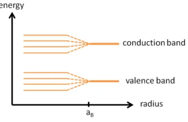
A quantum dots is known as a size is less than Bohr radius and whose exciton is squeezed and confined in a 3D semiconductor matrix, resulting in the quantum confinement [1-2]. Energy spectrum of a quantum dot can be engineered by changing the size, shape, and confinement potential [3]. For example, as the size of quantum dot is small enough, the energy band splits off like a discrete energy level of atoms, as shown in Figure 1-1. The energy levels can be calculated using a particle in a box model by Schrodinger equation and the energy of different states is dependent on the length of the box, i.e. the size of the quantum dot. Size and band gap are inversely dependent in quantum dots. It is said to be in ‘strong confinement regime’ as their radii are smaller than Bohr radius. The opposite in ‘weak confinement regime’, Coulomb potential of electron and hole can’t be neglected. While dimension scales to zero-dimension, the properties of physics of material are different from the classical. In optics, luminescence occurs as an electron in the excited state drops down to a lower level (or ground state) by radiative transition and recombines with the hole [4]. The emission wavelengths decreases with the smaller size of quantum dot, resulting in a color shift from red to blue in the light emitted.
Quantum effect in semiconductor nanocrystals has been a subject of extensive studies since the early 1980s. Quantum dots were discover by Alexei Ekimov in disperse crystalline phase of CuCl forms in the glass [5]. Louis Brus and Yosuke
Kayanuma derived the expressions of the energy in the limit of strong confinement and weak confinement of quantum dots in the last 1980s [6-8]. In 1991, the change in the color of colloidal solutions of semiconductor was discussed by Rosetti et al. [9]. Over the last two decades, theoretical and experimental research on these nanoparticles has increased significantly in order to explore many basic properties of quantum dots and attracted by commercialization efforts [10]. Quantum dots are widely applied in light emitting diodes (LED), diode laser, solar cells, and bio-sensors. [11]. For example, in 2012, conversion efficiency of 50.3% was predicted for the novel Si-based intermediate band solar cell (IBSC, shown in Figure 1-2) using high periodic silicon nanodisk array by Samukawa et.al..[12] It is large improvement in the conversion efficiency of Si-based solar cell via quantum confinement effect.
1.2 Properties and Applications of ZnO
Zinc oxide (ZnO) is a promising candidate for short-wavelength optoelectronic devices due to its nature of wide direct bandgap (~ 3.37eV) and large exciton binding energy (~60meV). The binding energy of ZnO is much larger than that of GaN (~25meV) and ZnSe (~22meV), also larger than the thermal energy, which is the mechanical energy required to disassemble a whole electron-hole pair into separate parts. The efficient excitonic of ZnO occurs while the exciton binding energy is much greater than the thermal energy at room temperature (~26meV) [13-16] , it means that ZnO has higher emission efficiency than others. In addition, ZnO has several properties similar to GaN material, like as lattice constant and wide bandgap [17], as shown in Table 1-1. However, the exciton binding energy of ZnO is 2~3 times of GaN, and the emission efficiency in UV region is 18% in experiment also higher than 12%
of GaN-based LED fabricating by MOCVD [18].
ZnO in various forms, such as single crystals, powders, and films, has been prepared by many techniques since the realization of emission mechanism of ZnO in 1997 [19]. Figure 1-3 (a) shows many kinds of ZnO nanostructures, including nanoring, nanowire, and nanorod (Figure 1-3 (c) and (d)). Figure 1-3 (b) is the ZnO quantum dots [20]. Two of the main emissions of ZnO are ultraviolet (UV) emission from free exciton recombination and a broad visible emission associated with intrinsic or extrinsic defects. Figure1-4 illustrates all the emission of ZnO material in schematic band diagram. The growth of nanosized ZnO, including the ZnO quantum wells, ZnO nanowires, and ZnO quantum dots have been investigated widely and used as transparent conductors in solar cell, as components in UV light emitters and high-power electronics. Recently, ZnO nanostructures attracted attention for possible applications in optoelectronic and spintronic devices, such as light-emitting and laser diodes with polarized output, spin-based memory, and logic [15].
ZnO quantum dots are of great interest because of their unique optical properties and potential for device application. Different preparation methods have been established [21]. Wet chemical method likes sol-gel is the most widely popular. However, the drying of the product may result in the formation of secondary phase due to the large numbers of hydroxyl groups. The other preparation method with solvent-free includes magnetron sputtering [19, 21-22], ion implantation [23-24], and thermal evaporation [25]. However, the mostly dry depositions have the high-temperature process to fabricate the ZnO nanoparticles. Recently, the fabrication of ZnO nanocrystals via sputtering has been demonstrated with the main focus on the optical properties of the prepared composite systems. Rudolf Bratschitsch et al.
reported that ZnO quantum dots embedded in an amorphous silicon oxide by sputter successfully and demonstrated the apparent quantum effect [21, 26].
1.3 Motivation
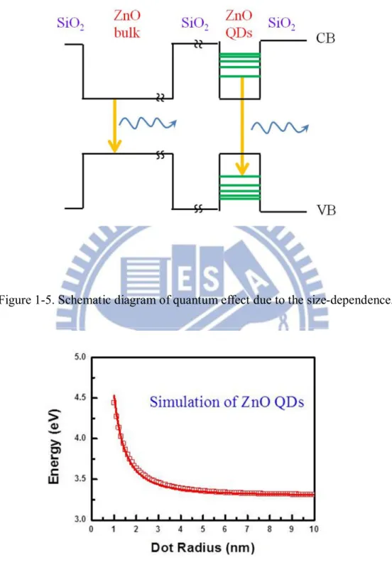
ZnO material is of considerable technology importance because of its nature of property is largely potential in UV emission. UV emission is widely applied in light emitting diodes for counterfeit detection, sterilization, printing, and illumination [27-29]. First, we expects that tunable energy bandgap could be controlled resulting in the size-dependence quantum confinement effect, as shows in Figure 1-5 and Figure 1-6. Figure 1-5 illustrates that energy band will discrete into discontinuous energy states as the dimension less than the Bohr radius of ZnO material. The energy distribution associated with the dot size in theoretical simulation is demonstrated in Figure 1-6. ZnO quantum dots or nanostructure have superior optical to the bulk owing to the quantum confinement effect, including the high emission efficiency and high output power. Because of the confined energy band, the recombination of quantized electrons and holes are improved significantly. Simultaneously, since the fast radiative recombination rate, the emission efficiency does not decrease as the more carriers input [4].
Several methods to fabricate ZnO nanostructures are illustrate in chapter 1-2, including the wet and dry deposited process. As usual, wet process is more complex, long-time, small production, and unstable. High-temperature annealing steps for the latter are necessary. In 2011, Rudolf Bratschitsch found out that ultra-low deposit rate using magnetron sputtering is effective technology to fabricate the ZnO quantum dots in amorphous silicon dioxide [26]. Therefore, magnetron sputtering system is
accepted to fabricate the size-dependent ZnO quantum dots in this thesis. The most advantage is that ZnO quantum dots are prepared by controlling the deposit rate without annealing process. Others include simple and stable process, and mass production.
1.4 Organization of the Thesis
In this thesis, we will discuss and understand the evolution of ZnO quantum dots. Chapter 2 covers the theoretical background of quantum effect, and fundamental optical transitions of semiconductors, such as absorption and excitons-relaxed emissions. In chapter 3, we describe the experimental details including the process of fabrication and analysis methods after measured. Two of methods of ZnO quantum dots embedded in SiO2 by magnetron sputtering will be investigated and discussed in
Table 1-1. Comparison of properties of ZnO with other wide bandgap semiconductors [17].
Figure 1-1. Splitting of energy levels for small quantum dots owing to the quantum confinement effect and aB is Bohr radius.
Figure 1-2. High efficiency of 50.3% for Si-based IBSC. (a) Schematic structure. (b) The device energy band diagram. (c) The efficiency contour plot depends on the
Figure 1-3. (a) Varietical ZnO nanostructures. (b) ZnO quantum dot. (c) and(d) are ZnO nanorods. [20]
Figure 1-5. Schematic diagram of quantum effect due to the size-dependence.
Chapter 2
Theoretical Background
2.1 Quantum Effect
During the last decade, quantum effect of semiconductor structure has been a subject of extensive studies. Quantum-size effect is one of that. A wide variety of materials has been growth as nanostructure with low-dimensional from three (bulk material) to the quasi-zero dimension. The quasi-zero dimension structures are usually called quantum dots (QDs). Quantum effect is most directly detected as the energy shift of the optical absorption and luminescence peak in the materials from few tens to few hundred in meV. The theoretical calculation of quantum confinement of interacting electron-hole in semiconductor was introduced in the last 1980s.
2.1.1 Quantum Effect
The model derived from the physical nature of cluster molecular orbital (MO) to solve Schrodinger equation using Hamiltonian [5-7]. The general wave function form of a Bloch theory is
kre ⃑∙ kr
kr + nµkr
The kis periodic function of unit cell with a relatively weak k dependence, and
than a unit cell. The quantum wave number k is infinitely delocalized in the limit of infinitely large crystallite.
The localized in space partial plane wave of the wave pocket of Bloch MOs is shown in the Fourier transform,
ir⃑∑ ∫ f (k)r⃑dk
Consider the sample example as k=0 at the bottom of conduction band in E-K band structure, and ignore the weak k dependence of . The ir⃑is only dominated
by k state from the conduction band as the cluster is not too small. And the expectation value of electron energy of size-dependence quantum effect is
Ei = | < i Hi > | ≈ E + ∑ , , [ ]
Here only keep the lowest order nonzero term in Taylor’s series expansion for energy and the cluster is considered as a spherical symmetry to ignore the later terms. The effective mass tensor is shown as
Mi,j = h
4π
Where h is Planck constant. For the most semiconductor, the effect mass me near
k=0 of conduction band is taken due to the isotropic tensor with average diagonal element. Here get the energy form as
E ≈ E + h 8m R
contributed to the second term on the right hand. It is like a particle in a box. There is only considered about a single electron on the bottom of conduction band above. However, it is more complex to consider the hole on the top of valence band, spin, spin-orbit interaction, and the perturbation. The later results in the energy band degenerate. Considering the shielded Coulomb interaction, the model of Hamiltonian for the cluster’s lowest excited state is corrected as
H = ∇ ∇ −
| |+ polarization terms
An analytical approximation for the first excited state is
E∗( ) ≅ E ( )+ + – . + smaller terms
Where E∗( ) and E ( ) are the energy bandgap of the quantum dots and bulk materials. R is the radius of clusters (quantum dots), me and mh are the effective
mass of electrons and holes, and ϵ is dielectric constant.
This formula is based on weak Coulomb interaction and showed an expression of the energy of first excited state (i.e. the lowest eigenstate) in the limit of the strong confinement. It resulted in a lower energy as the Coulomb term R-1 dominated, a higher energy as the quantum localization term R-2. As long as the quantum size is small enough, the energy bandgap will increase apparently.
2.2 Optical Principles
2.2.1 Direct Bandgap Semiconductor
In solid state physics, the bandgap of semiconductor is including direct and indirect [4]. The difference of them is depended on the relative position of the conduction band minimum and the valence band maximum on E-K diagram in the Brillouin Zone (B.Z.), as shown in Figure 2-1. Figure 2-1(a) illustrates the direct gap, both are k=0 or the same value of k at the B.Z. center, while Figure 2-1(b) shows the indirect gap with the conduction band maximum does not occur at k=0, but rather at some other value of k. It means that the transition of indirect gap material must involve a phonon to conserve momentum. In other words, the transition of a direct gap material occurs without any phonons being involved.
2.2.2 Optical Absorption
Optical absorption occurs possibly as the photon energy is larger than the bandgap Eg between the lower band and the final state of the upper band [4]. Those
bands must satisfy the selection rules and Pauli exclusion principle demands during the interband transition. Figure2-2 illustrates the transition, and the relative law of conservation of energy shows as followed,
Ef = Ei+ hν
where Ei is the energy of electron in the lower band, Ef is the energy of the final state
in the upper band, and hνis the photon energy. This is implies that the absorption shows a threshold behavior: interband transitions will not be possible unless hν > E .
The optical absorption is quantified by its absorption coefficient , and assuming a direct transition for semiconductor with parabolic bands. The absorption coefficient can be described with the different powers of the absorption coefficient against photo energy for direct and indirect bandgap material. is related to photon energy according to the following formula,
α ∗ (hν) ∝ (hν − E ) / , for direct bandgap α∗ (hν) ∝ (hν − E ) , for indirect bandgap
This is a common and simple method to distinguish whether a bandgap is direct or indirect by using absorption spectroscopy.
2.2.3 Photoluminescence (PL)
In solids, the reverse process of absorption of radiative emission in which electrons in an excited state drop down to the lower level by emitting photons is called luminescence. Interband luminescence occurs in a semiconductor when a excited electron at conduction band drop back to the valence band by the emission of a photon. This simultaneously reduces the number of electrons in the conduction band and holes in valence band by one. It corresponds to the annihilation of an electron-hole pair, and is known as radiative electron-hole recombination. Direct bandgap material has a superiority to emitting a photon owing to that the electron and hole recombine must have the same k-vector. The luminescence spectrum usually consists of a narrow emission line close to the bandgap energy. As for indirect bandgap material, a phonon must be emitted or absorbed when the photon is emitted. Therefore indirect bandgap materials are rarely applied as light emitters.
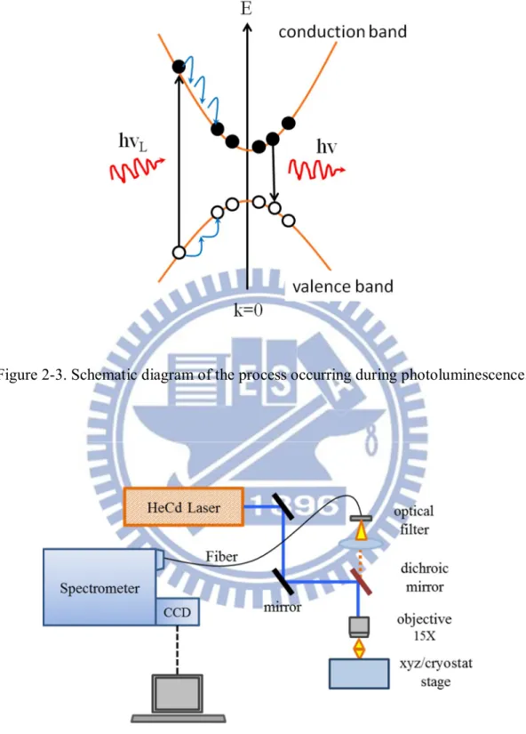
Photoluminescence is one of all the mechanisms of luminescence. The light re-emits after absorbing a photon of higher energy than bandgap Eg. Each step
corresponds to the emission of a photon with the correct energy and momentum to satisfy the conservation laws. Generally excited electrons do not remain in these state high up in conduction band, because they can loss its energy very quickly by emitting phonons. The same conditions apply to the relaxation of the holes in the valence band. They have enough time to relax to the bottom of their band before emitting photons, as indicated in Figure 2-3. The process occurring during photoluminescence in a direct gap semiconductor after excitation at frequency vL.
Photoluminescence spectra can be recorded with an experimental arrangement such as the one shown in Figure2-4. The sample is mounted in a variable temperature cryostat and is illuminated with a laser or bright lamp with photon energy greater than Eg. If a liquid helium cryostat is used, sample temperatures from 2K
upwards are easily obtained. The luminescence is emitted at lower frequencies and in all directions. A portion is collected with a lens and focused onto the entrance slit of a spectrometer. The spectrum is recorded by scanning the spectrometer and measuring the intensity at each wavelength with a sensitive detector such as a photomultiplier tube. Alternatively, the whole spectrum is recorded at once using an array of detectors such as a charge coupled device (CCD).
Figure 2-1. Interband transitions in solids: (a) direct bandgap, (b) indirect bandgap.
Figure 2-2. Interband optical absorption between an initial state of energy Ei in an
Figure 2-3. Schematic diagram of the process occurring during photoluminescence.
Figure 2-4. Experimental arrangement used for the observation of photoluminescence spectra. .
Chapter 3
Experimental Details of Fabrication and
Analysis Systems
3.1 Experimental process
In this thesis, we fabricates the sample of ZnO Quantum dots embedded in SiO2
using the magnetron sputter. Two of structures to fabricate are ZnO QDs-SiO2
nanocomposite films by co-sputtering and ZnO-SiO2 multilayer structures, as shown
in Figure 3-1 and Figure 3-2. Figure 3-1 illustrates ZnO and SiO2 targets are sputtered
simultaneously and the schematic diagram of the structure with ZnO QDs-SiO2
nanocomposite films. The later with forty alternating layers is that sputtering ZnO and SiO2 films with ultra-thin thickness separately and showing schematic diagram of the
structure in Figure 3-2.
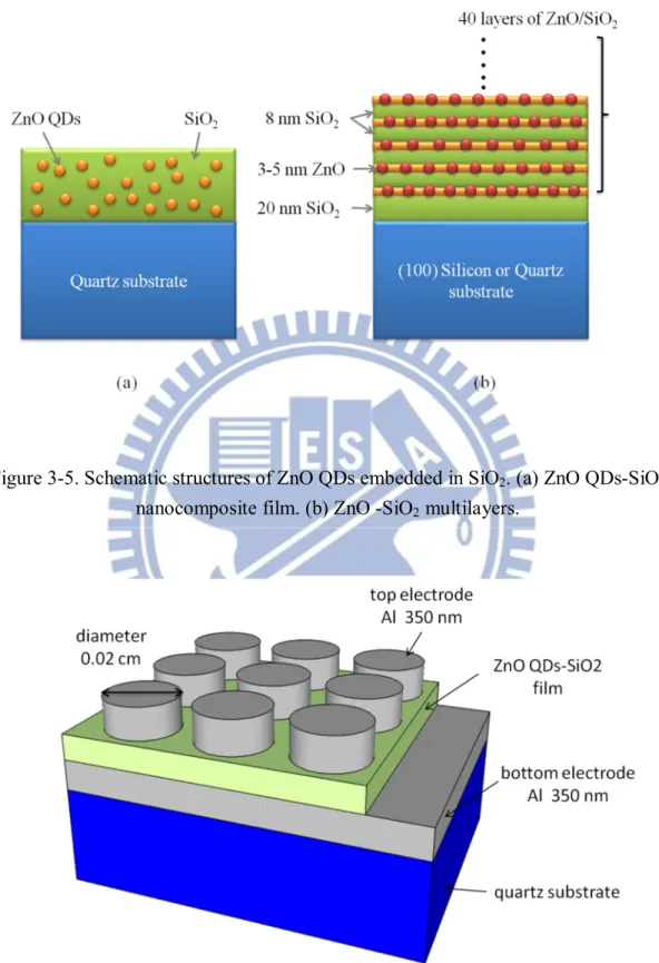
The experimental process of this study is shown in Figure 3-3, fabrication and measurement are described as follows. Before depositing, processes of substrates cleaning are described as the chart in Figure 3-4. The sample I structure is shown in Fig.3-5. First, a SiO2 bottom layer of 20 nm thickness is deposited onto the (100)
silicon and quartz substrates to eliminate any influence of the substrates on growth of the quantum dots. It is formed by plasma-enhanced chemical vapor deposition (PECVD, OXFORD INSTRUMENTS, Plasmalab80Plus) at 300℃. The sample with ZnO QDs-SiO2 nanocomposite film is excluded. The bottom layer is followed by
transmission electron microscopy (HRTEM), and 100 nm SiO2 passivation layer is
deposited by PECVD for reducing the damage from focus ion beam (FIB).
In measurement of electrical property, the samples are fabrication into a sandwiched structure (Sample II) on quartz with a top and bottom electrode of Al. It is without 20nm SiO2 bottom layer. The Al electrode is deposited by the thermal
evaporation coater with a thickness of 350 nm. Figure 3-6 illustrates the schematic of the sample II in the sandwiched for the purpose of the electrical measurement.
3.2 Magnetron Sputtering
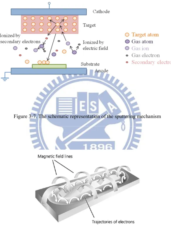
The basic sputtering principle is described as followed, the accelerated ion to bombard the target surface, sputtering neutral atom on the substrate surface, and deposit. Figure 3-7 is the schematic diagram of sputtering process. Neutral gas is ionized to form ions and electrons by electric field from DC/RF power supply. Ions with high-energy accelerate and bombard to the target upon the cathode, and the sputter atoms and secondary electrons eject. As secondary electrons have sufficient energy to ionize the gas atom/molecules, the probability of oscillation will increase, resulting in the greater deposit rate. [30-34]
As the affect of magnetic field, which parallel to the target surface, the motion of secondary electron is constrained to the region upon target, increasing the probability of gas atomic ionization by secondary electrons, and intensifying the ion bombardment, as shown in Figure 3-8. Magnetron sputtering overcame the other limitation of basic sputter, e.g. low deposition, and high substrate heating effect.
In addition, for ensure the atom of material can move freely towards the substrate, the low pressure of vacuum condition is necessary. Low pressure leads to the long mean-free-path (MFP). As MFP is more, the probability of atom travel without colliding with another gas atom is more, i.e. it avoids that too many atom-gas collisions after ejection from the target.
Here, both two structures of ZnO QDs-SiO2 nanocomposite film and ZnO
QDs-SiO2 multilayer are deposited on (100) silicon and quartz substrates by
sputtering ZnO and SiO2 target. The base pressure of the deposited is 8×10⁻⁷ Torr in a
high vacuum. ZnO target is sputtered using DC power supply, and SiO2 is an insulator
resulting in it must be sputtered using RF power supply. The entire deposition process is carried out at room-temperature without annealing of substrates.
3.3 Scanning Electron Microscopy (SEM)
Scanning electron Microscopy (SEM, Hitachi S-4700I) is used for examining the thickness of ZnO QDs-SiO2 nanocomposite films. SEM is one of electron
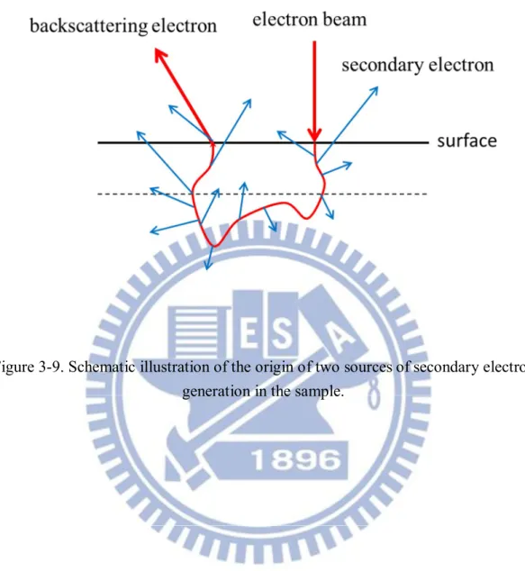
microscopes, it used a focused electron beam that interact with the sample to produce an image [35-36]. The signals depend on the atomic structure, shape, and conductivity of materials. The main interacting electrons are collected to reveal the morphology of samples, which is including the secondary electrons, and backscattered electrons. Those produces as focused electron beam hits atoms on the surface, those reflected are called backscattered electrons. The atoms must give off another electron (secondary electron) or emit light for conversation, and becoming stable. The interaction between incident electron beam and sample surface is illustrated as Figure3-9.
A SEM column consists of an electron gun, one or two condenser lenses, an objective aperture, and an objective lens. The electron gun produces a source of electron and accelerates the electrons to energy of 0.5~30 keV. This occurs in a vacuum environment ranging from 10-4 to 10-10 Torr. The electron lenses in the column are used to demagnify the image of the gun crossover and focus a final spot on the specimen on the order of 1nm ~ 1m with a beam current in the range of 1pA ~ 1A. The condenser lens controls the amount of demagnification and the probe forming or objective lens focuses the final probe on the specimen. A schematic of a typical SEM is shown in Figure 3-10.
The lens and aperture system in the column provide control of the beam through manipulation of the probe diameter, probe current, and convergence angle. These three parameters can be controlled and used to achieve high depth-of-field, high-resolution, or high beam current for x-ray microanalysis. A small convergence angle is needed for high depth-of-field imaging and can be obtained with a small objective aperture and a long working distance. High resolution imaging requires a small probe size which can be obtained with a strong condenser lens, an objective aperture, and a short working distance. Finally, x-ray microanalysis may require higher beam currents which can be obtained by weakening the condenser lens and removing the objective aperture.
3.4 Transmission Electron Microscopy (TEM)
The transmission electron microscopy (TEM) is a microscopy technique using tunneling electron beam directly through an ultra-thin specimen and image forming from electrons scattering into discrete diffracted beams [37-38]. The diffracted electron beams are then focus in the back focal plane of objective lens. Generally, a TEM is composed of several components, includes a vacuum system in which the electrons travel, an electron emission source for generation of the electron stream, a series of electromagnetic lenses, as well as electrostatic plates. The latter two allow the operator to guide and manipulate the beam as required. Also required is a device to allow the insertion into, motion within, and removal of specimens from the beam path. Imaging devices are subsequently used to create an image from the electrons that exit the system. The detail components are shown in Figure 3-11.
Diffraction mode and image mode are two modes of TEM, as shown in Figure 3-12. When operated in diffraction mode, the diffraction lens is focused on the back focal plane to produce a diffraction pattern. For the imaging mode, the diffraction lens is focused on the first image plane to produce a magnified image. In addition, the beam may be allowed to pass through the sample to obtain a bright-field image however the diffracted beams produce a dark-field image.
The interaction of the electron beam with crystalline material tends to be by diffraction. The orientation of the planes of atoms in the crystal to the electron beam changes the intensity of diffraction. TEM equipment often uses a goniometer to allow the sample to be tilted to a range of angles to obtain specific diffraction conditions.
Diffracted electrons are also selected using different apertures.
The intensity of diffraction is a maximum at the Bragg angle, although a variation of diffraction intensity occurs with deviation from the Bragg 37 angle. This also depends on the thickness of the specimen. The thinner the crystal sample, the further the crystal may deviate from the Bragg condition.
When crystal planes are almost parallel to the electron beam they are close to fulfilling Bragg’s Law. The majority of electrons are diffracted when the electron beam strikes one set of lattice planes exactly at their Bragg angle and only a few will pass through the sample undeviated. If the planes are exactly at the Bragg condition, strong diffraction will occur and the bright field image will appear dark. This variation with diffraction is shown with bend contours which are a feature of bending of the crystal planes. Dark contour images correspond to regions at the Bragg angle, while light contours result in the regions not strongly diffracting.
In this study, TEM system (JEOL, JEM-2100F) is used to image the ZnO quantum dots, which with 0.23 nm of point image, 0.14 nm of lattice image for resolution.
3.5 X-ray Diffractometer (XRD)
X-ray diffraction (XRD) is a powerful tool with non-destructive for investigating the crystalline structure, chemical composition, and physical properties of materials, which those cause a beam of X-rays to diffract into many specific directions. The first XRD patterns of rock salt were obtained in 1911 [39]. For semiconductor, XRD is
mainly use to evaluate the quality of the film, determine the mole fraction of alloys, and investigate the thickness and fine structure of materials with superlattice structures.
This analytics technique of XRD is based on observing the diffraction intensity of an X-ray beam hitting a sample as a function of incident and diffracted angle, wavelength, energy, and polarization. Crystals are regular arrays of atoms, and X-ray can be considered as waves of electromagnetic radiation. Atoms scatter X-ray waves, primarily through the atom’s electrons, like that an ocean wave striking a lighthouse produces secondary circular wave emanating from the lighthouse. Resulting in elastic scattering, an X-ray striking an electron produces secondary spherical waves emanating from the electron. [36] A regular array of scatters produces a regular array of spherical waves. Although these waves cancel one another out in most directions through destructive interference, they add constructively in a few specific directions. It follows the Bragg’s law,
2d sin= n
Here d is the spacing between diffracting plane, is the incident angle between the incidence and the reflect X-ray, n is any integer, and is the wavelength of the incident X-ray beam. Figure 3-13 shows the schematic diagram of Bragg diffraction. X-ray diffraction results from an electromagnetic wave (the X-ray) impinging on a regular array of scatters (the repeating arrangement of atoms within the crystal).
In our measurement system the X-ray diffraction (Bede, D1) was characterized using -2 mode to identification the structures of ZnO quantum dots embedded in SiO2.
3.6 UV/VIS/NIR Spectrophotometer
Measurements of the optical transmittance and reflectivity in the visible and ultra-violet are performed to characterize the optical absorption. Optical absorption is calculated using the formula as followed [40].
α =1 dln
T (1 − R ) T
Here, is absorption coefficient, d is the thickness of film, TQ is transmittance of
quartz substrate, and TS, TR are transmittance and reflectivity of sample. Figure 3-14
illustrated the optical path of the UV/VIS/NIR spectrophotometer system (Hitachi U-4100) with beam size is 5×5 mm2.
3.7 Photoluminescence System (PL)
Photoluminescence (PL) spectroscopy has been used as a measurement method to detect the optical properties of materials because of its nondestructive characteristics. PL is the emission of light from a material under optical excition, more details are explained in the section 2.2.3. The setup of our PL system is described as followed. A 325nm He-Cd continuous wave (cw) laser with 30 mW of incident power (in time average) is used to measure at room-temperature, which is with a edge filter to clear the spectrum of laser. The laser beam is delivered to the sample surface in normal direction by a 15X UV microscope objective. The pump spot at sample surface had a Gaussian intensity profile with 1/e2 diameter of 50 μm, verified by a knife-edge measurement. The photoluminescence (PL) spectrum was
collected by the same UV objective and coupled into an optical fiber connected to the input of a spectrometer (Jobin Yvon IHR320)
3.8 Electrical Measurement
A semiconductor parameter analyzer of model Kethley 4200 is utilized to measure the current-voltage (J-V) characteristics of sample II. The resulted current from an increasing voltage is examined, and the limit current is 0.1A.
Figure 3-1. (a) Co-sputtering system. (b) Structure of ZnO QDs-SiO2 nanocomposite
film.
Figure 3-2. (a)System of sputtering ZnO and SiO2, respectively. (b) Structure of ZnO
Figure 3-3. Experimental Process.
Figure 3-5. Schematic structures of ZnO QDs embedded in SiO2. (a) ZnO QDs-SiO2
nanocomposite film. (b) ZnO -SiO2 multilayers.
Figure 3-7. The schematic representation of the sputtering mechanism
Figure 3-8. The principle of magnetron sputtering. Electrons are trapped by the Lorentz force K= e (v × B) in an inhomogeneous magnetic field, resulting in an
Figure 3-9. Schematic illustration of the origin of two sources of secondary electron generation in the sample.
Figure 3-12. Ray diagram showing two basic operations of TEM. (a) Imaging projecting a diffraction pattern and (b) projection of an image onto a viewing screen.
Figure 3.13. Diagram of Bragg’s diffraction.
Chapter 4
ZnO
xQDs-SiO
2Nanocomposite Film by Co-
sputtering
4.1 Fabrication of ZnO
xQDs-SiO
2NanocompositeFilm
ZnOx QDs- SiO2 nanocomposite films with dot diameter from 3 nm to 7 nm were
prepared via co-sputtering method. The schematic diagram of ZnOx QDs-SiO2
nanocomposite films is shown in Figure 4-1. First, quartz substrates are cleaned before the sputtering. High purity ZnO target and SiO2 target are placed on the
deposited chamber with base pressure of the deposited is 8×10⁻⁷Torr in a high vacuum. The entire deposition process is carried out at room-temperature without annealing of substrates. ZnO and SiO2 are deposited simultaneously using the co-sputtered system
to produce ZnO quantum dots in an amorphous silicon oxide. In order to form the smaller ZnO quantum dots and expand the relative deposit rate, we set the smallest DC power of 40W for ZnO and largest RF power of 200W for SiO2 in the limit of
sputtering system as possible. During sputtering process, the flow rate of argon is controlled as 30 SCCM, pressure is kept at 5, 10, 20mTorr for obtaining the various ZnO contents, and the detail deposited conditions are shown in Table 4-1. The relative deposit rate is defined as
R = D D
Here, R is relative deposit rate, DZnO, DSiO2 are represented as the deposit rate of
ZnO and SiO2, respectively, and R5>R20>R10.
4.2 Structure Morphology
At first, thickness and morphology of ZnOx QDs-SiO2 nanocomposite films is
identified by scanning electron microscopy (SEM) to ensure the growth of nanocomposite films. Figure 4-2 is a SEM image of depositing pressure of 5mTorr. The microstructures are examined by tunneling electron microscopy (TEM). Figure 4-3 presents the TEM micrographs of conditions with depositing pressure of 5mTorr, and shows a better result compared to other conditions. It can be clearly seen that ZnO forms QDs with diameter form 3nm to 7nm embedded in amorphous silicon oxide. Figure 4-3(a) reveals the all-area of ZnOx QDs-SiO2 nanocomposite film, and the
image zooming out is shown in Figure 4-3(b). Bright-field and dark-field of same region from TEM sample are used to identify the formation of ZnO nanocrystals, as illustrated in Figure 4-3(c) and Figure 4-3(d). According to the TEM images, we find out that ZnO quantum dots are formed in random diameter no matter how we vary the working pressure from 5mTorr to 20mTorr to decrease the relative deposit rate. It cans not be accurately controlling in the ZnO quantum dots size on ZnOx QDs-SiO2
nanocomposite films. But isolated ZnO nanocrystals are well confined in amorphous SiO2 surrounding.
In addition, with the measurement of the X-ray diffraction, we find that no signal distribution in special direction of ZnO nanocrystal, as shows in Figure 4-4. Compared to the ZnO film with 100nm of thickness, it is obvious that exhibiting of
two peaks around 34.4° and 62.8, related to (002) and (103) planes, respectively [41]. The peaks are indexed from the standard value of bulk ZnO. (JCPDS card No 36-1451). Owing to the wurtzite ZnO material has the c-axis preferential growth characteristics. However, there are no obvious peaks of XRD result for nanocomposite film, it is very weak diffraction signal. According to the data, we assume the ZnO nanocrystals are covered in amorphous silicon dioxide, random c-axis growth, and few content of ZnO material, those result the negligible diffraction signal of ZnOx QDs-SiO2 nanocomposite film.
4.3 Characteristics of ZnO
xQDs-SiO
2Nanocomposite Film
To investigate the optical properties of ZnOx QDs-SiO2, the measurements of the
optical transmittance in the visible to UV are performed on the transparent quartz substrates. Figure 4-5 shows (hv)2 as a function of photon enegy hv, calculated from the optical transmittance spectrum, where denotes the absorption coefficient. In this absorption spectrum, we could not define the energy bandgap by the intercept of absorption curve as the result of the broad absorption starting from 2.6eV to near 5eV. Absorbing from ZnO defects (under 3.26eV of bangap of ZnO film in this study), absorbing by ZnO quantum dots (above 3.26eV of energy values), and absorbing of amorphous SiO2 defects (near 5-6eV) which are those causes the weak absorption [16,
42-43]. The broad absorption band around 5-6eV is associated with the peroxyl radical, for the first time. Another absorption band of SiO2 is 7.6eV, which is not
shown in the spectrum. Even if the energy above 3.26eV is corresponded to the absorbing of ZnO quantum dots, we still could not define the energy bandgap with the size-dependent quantum effect.
Figure 4-6 shows a typical room-temperature photoluminescence (PL) spectrum recorded from 5mTorr to 20mTorr, which is normalized. The differences between those samples are only slight at the intensity of PL signal, and those distributions are almost same, no energy change on the maximum by varying the relative deposit rate. It is perhaps that random size of ZnO QDs results the similar results in different process conditions. At the same time, the full width at half maximum (FWHM) of 100nm ZnO film has the minimum value, it appears the quality of ZnO materials. FWHM increasing follows the 10mtorr, 5mtorr and 20mtorr. In addition, compared to the absorption spectra (Figure 4-5), the emission only occurs around 2.5-3.5eV. It demonstrates that defect absorption and emission of ZnO are near 3eV of energy, and near band edge absorption and emission are around 3.2-3.5eV, resulting in the direct bandgap of zinc oxide property. However, the minimum near 3.5eV in PL spectrum illustrates few photons emit with photon energy above 3.5eV, but the strong absorption occurs. We therefore expect nanocomposite film strongly absorb starting from 3.5eV owing to the defect of amorphous SiO2.
Finally, the dark I-V curves of ZnOx QDs-SiO2 nanocomposite film (Sample II)
are shown in Figure 4-7. As the ZnO QDs are well-coating in SiO2 in 5mTorr of
working pressure, the conductivity is very low relatively. We assume that conductivity is larger and stronger absorption occurs while the contents of direct bandgap ZnO are more. So we observe the opposite tendency in Figure 4-5 and Figure 4-7.
4.4 Summary
In summary, ZnOx QDs-SiO2 nanocomposite films are formed by co-sputtering
confined in amorphous silicon oxide as shown in the image of TEM. From the analysis, we discuss the issues of nanocomposite film, including the low content, random size, random c-axis growth and absorbing from defects of SiO2. In addition, it
is only slightly blue-shift between ZnO film and nanocomposite film, and no-shift by controlling the relative deposit rate as expected. This system is more complex, and it is worth to study. Finally, although there are no direct evidences of size-dependent quantum effect, but we did successfully fabricate the isolated single ZnO quantum dot in an amorphous silicon dioxide.
Working pressure (mTorr) DZnO (A/s) DSiO2 (A/s)
Relative Deposit Rate R
5 0.14 0.32 0.43
10 0.08 0.30 0.27
20 0.05 0.17 0.29
Figure 4-1. The schematic diagram of ZnO QDs- SiO2 nanocomposite films.
Figure 4-3. The TEM images with working pressure of 5mTorr. (a)-(b) isolated ZnO nanocrystals embeds in amorphous SiO2,
30 40 50 60 70 (103) 2(degree) In te n s ity ( a .u .) (002) Nanocomposite film ZnO film
Figure 4-4. Comparison XRD pattern of 100nm ZnO film and nanocomposite film.
2 3 4 5 6 0.0 5.0 10.0 15.0 5 mTorr 10 mTorr 20 mTorr ( h v ) 2 (1 0 5 e V /c m ) 2 Energy (eV) 20.0
Figure 4- 6.The PL spectra with working pressure of 5, 10, 20mTorr and 100nm ZnO film. The longitudinal line is the energy corresponded to the maximum signal.
Chapter 5
ZnO quantum dots embedded in SiO
2by
Making ZnO-SiO
2Multilayer Structures
5.1 Procedure of ZnO-SiO
2multilayers
ZnO quantum dots are fabricated by magnetron sputtering of ZnO and SiO2
multilayers onto (100) silicon and quartz substrates after cleaning process and a SiO2
bottom layer depositing. Figure 5-1 illustrates the schematic diagram of ZnO-SiO2
multilayers structure. Like the conditions of nanocomposite film deposited, a high vacuum base pressure of 8 × 10⁻⁷ Torr ensures a stable and clean deposition environment, and no annealing process. The sputtering process is carried out in argon (30 SCCM) atmosphere, and the working pressure is kept at 5mTorr. ZnO and SiO2
targets are used at sputtering powers of 60W (DC) and 200W (RF), and deposit rate are 0.15A/s and 0.38A/s, respectively. We turn off the argon gas and pump for 3 min before the next layer deposited. An integrate structure are composed by forty alternating layers of ZnO (from 3nm to 5nm in nominal thickness) and SiO2 (8nm in
nominal thickness).
In this chapter, we study the characteristics of ZnO quantum dots embedded in amorphous silicon oxide by ZnO-SiO2 multilayer structure. The nanostructures of the
samples are analyzed by transmittance electron microscopy (TEM), and X-ray diffraction (XRD). To characterize the optical and electric properties, absorption, emission, and current-voltage curve are measured. In addition, the post-annealing
samples are discussed and compared to as-grown samples. Finally, we calculate the quantum dot effect of ZnO QDs in SiO2 using finite element method (FEM).
5.2 Structure Morphology
Nanostructural investigations of the sputter-deposited ZnO quantum dots are perfprmed by TEM. Figure 5-2 shows a representative HRTEM image of the nominally 3nm, 4nm, and 5nm-thick ZnO layers embedded in amorphous SiO2. ZnO
quantum dots may be identified as dark regions within the bright SiO2 surroundings.
Compared to the amorphous SiO2, the dark ZnO regions show a stripe-like structure
proving the crystallinity if the material. ZnO regions appear as connected-like layers with ZnO nanocrystal clusters. The diameters of ZnO nanocrystals are estimated from these HRTEM images, which are 3.9 nm, 4.6 nm, and 5.6nm in real thickness of average values, respectively.
The crystalline property of ZnO matrix has strong influences on the optical and electrical properties of ZnO layers. To get more information on the degree of crystallinity, the XRD measurement is carried out. Figure 5-3 shows the XRD of the 2q range from 30° to 60° of 100nm ZnO film and ZnO-SiO2 multilayers with various
thickness of ZnO layer. According to the JCPDS cards (No. 36-1451), the observed diffraction peaks are identified. The (002) plane is contributed from the c-axis preferred orientation of ZnO material. As thickness increases, the intensity of (002) peak will increase simultaneously, as shows in Figure 5-3(a). However, the intensities of ZnO (002) peaks are weak relatively in the multilayer structures, owing to the size effect and contributions of random c-axis. The full width at half maximum (FWHM)
become more broadly with the smaller thickness. In 3.9 nm real thickness, it has the most broad and weak intensity of (002) peak.
5.3 Characteristics of ZnO-SiO
2Multilayers
5.3.1 Optical Absorption
Optical characteristics are mainly studied in this section. Figure 5-4 shows (hv)2 as a function of photon energy hv, extracts from the transmittance and reflectivity by
α =1 dln
T (1 − R ) T
and changes with the thickness. Size-dependence of ZnO quantum dots is confirmed as the energy shifts. Evaluation of the optical transmittance and reflectivity of the 100nm ZnO layer results in a bandgap of Eg = 3.26eV (not shown), and Eg = 3.39eV, 3.36eV, and 3.33eV for 3.9nm, 4.6nm, 5.6nm ZnO QDs, respectively. When comparing the two retrieved bandgap values for ZnO film and ZnO QDs, we find a large blue-shift of 130meV between 3.9nm ZnO QDs and 100nm ZnO film, which is more excellent than before. In addition, the sample anneals at 550℃, and in nitrogen atmosphere (3SLM) for 30 minutes. The UV-visible absorption spectra are shown in Figure 5-5. The size of the ZnO QDs increases after annealing process, the characteristic absorption peaks for the synthesized ZnO QDs red-shift, as indicated in Figure 5-6. The size of ZnO quantum dots vary from 3.9nm to 4.3nm in average diameter after annealing, which are calculated from TEM images. However, 100 nm ZnO film is thick enough so that the bandgap are all the same to the samples of
as-deposit and post-annealing.
5.3.2 Photoluminescence
To demonstrate the ability of the sputtered quantum dots to serve as light emitters in UV, we perform photoluminescence emission measurements at room-temperature. The PL spectra of ZnO-SiO2 multilayer with variety sizes from 3.9 nm to 5.6 nm
(3nm-5nm nominal thickness) are shown in Figure 5-7. The broad PL peaks spread at near 3.32-3.38eV. Similar to transmittance measurements, the photoluminescence emission of the quantum dots shows a prominent blue-shift compared to PL emission of 3.16eV of 100nm ZnO layer. It is obvious in Figure 5-8, as generally kown in semiconductors, such as GaN and ZnO, the formation of QDs causes a blue-shift in the PL spectra due to quantum confinement. The UV emission is usually attributed to free exciton transitions [4, 13], and the FWHM reveal the quality crystallinity of the samples. In Figure 5-9, the annealed sample is compared to the as-deposit of 3nm nominal thickness ZnO layer. Because the larger size of ZnO QDs, the intensity becomes weakly and red shifts. The additional broad emission band in the visible region of the spectrum is attributed to electron–hole recombination of zinc interstitials [44].
5.3.3 Stokes Shift
Comparing the results of absorption and PL emission, in most samples, there are some interesting. We not only find energy shifts of the onset of absorption and UV PL emission of the ZnO QDs with respect to bulk material. We also observe a “Stokes shift”, i.e. an energy difference between absorption and emission of the quantum dots [4]. The Stokes shift is explained by applying the law of conservation of energy to the process. It is easy to see that in Figure 5-10, the energy of the photon emitted must be
less than that of the photon absorbed, and hence that the frequency of the emitted light is less than that of the absorbed light. The magnitude of the Stokes shift is therefore determined by energy levels of the atoms in the medium. In the experimental results, we can see the most significant energy difference in annealed sample of 3nm nominal thickness, as shown in Figure 5-11. The contrasts of other samples both as-deposit and post-annealing are appeared in Figure 5-12.
5.4 Simulation of the Quantum Dot Effect Using Finite
Element Method (FEM)
In this section, finite element method (FEM) is used to solve the calculating problems. FEM is a numerical technique for finding approximate solutions to boundary value problems in mathematic. It uses variational methods (the calculus of variations) to minimize an error function and produce a stable solution. The calculus model computes the electronic states for a quantum dot system, which is inspired largely by the work of Dr. M. Willatzen, Dr. R. Melnik, and B. Lassen [45].
Quantum dots can have many geometries including cylindrical, conical, or pyramidal. This model computes the electronic states of a conical ZnO quantum dots embedded in the SiO2 surrounding matrix, and we must solve the 1-band Schrodinger
equation in the effective mass approximation:
Where h is the Planck’s constants, Ψis the wave function, E is the eigenvalue r V r r E r m h e ) ( ) ( ))) ( ) ( 1 ( ( 8 2 2
(energy), and me is the effective mass (to account for screening effects). To simplify
the equation in term of
Separating the total wave function Ψ into
where φis the azimuthal angle. Then rewrite the Schrodinger equation in cylindrical coordinates as
Dividing this equation by
and rearranging its terms lead to the two independent equations
(1)
and
(2)
Equation 1 has obvious solutions of the form
V E m h ) 8 ( 2 2 ) ( ) , ( z r d v E d r m h r m r r r z m z h e e e 2 2 2 2 2 2 2 8 )] ( 1 ) 1 ( [ 8 ) ( ) , ( 2 r m r z e 2 2 2 1 d d 2 2 2 2 2 2 2 8 ] [ ] 1 ) ( 1 1 ) 1 ( [ 8 h E V r m r m r r r z m z h r m e e e e ] exp[i
where the periodicity condition (+2p)= implies that , the principal quantum number, must be an integer. It remains to solve Equation 2, which we can rewrite as
Note that this is an instance of a partial differential equation (PDE) on coefficient form,
where the nonzero coefficient are
This exercise models the eigenvalues for the four lowest electronic energy levels for the principal quantum number =0.
To solve this problem, use the Coefficient Form PDE interface. The model solves an eigenvalus/eigenfunction, for which we input the appropriate physical data and constants. The electron affinity of ZnO and SiO2 are 4.5eV and 1.0eV separately,
which is defined instead as the energy obtained by moving an electron from the vacuum level just outside the semiconductor to the bottom of the conduction band just inside the semiconductor, in the field of solid state physics. The energy bandgap are well known as 9.0eV for SiO2 and 3.37eV for ZnO. According to those constants, we
calculate the potential barrier is 3.5eV for quantized conduction band energy, and 2.2eV for confined valence band energy. In addition, the electron and hole effective mass are 0.24m0 and 1.21m0 for ZnO, and 0.3m0 and 1.0m0 for SiO2, respectively
[46-51]. Figure 5-13 is the schematic diagram of simulation system. The energy bands ) , 8 ( )] ( 1 ) 1 ( [ 8 2 2 2 2 2 2 V E r m h r m r r r z m z h e e e u u u u- ) d c (- . E and , 1 d , r 1 8 , V 8 , 8 2 2 r 2 2 2 2 2 2 e e e m h r m h m h c
of ZnO QDs in SiO2surrounging are splitting and discrete into energy states, as shown
in Figure 5-14. Followed are calculated with the lowest states, i.e. the ground state, Ec1 and Ev1. Here, we ignore the selection rule, which determines the allowed and forbidden states to transit.
Figure 5-15 compares both the experimental data and calculation in the dependence of the bandgap versus the ZnO QDs diameter, which indicates the same tendency of energy bandgap owing to size-dependent quantum effect. The calculation is based on the isolated single quantum dots in amorphous SiO2 surrounding.
Enlargement effect is expected to be predominant when the ZnO QDs size is less than the 5nm of double Bohr radius. Both absorption data and PL data are not fixed the result of simulation. For absorption data, it is the cluster of ZnO QDs in SiO2, not
isolated single QDs. Owing to the coupling of the neighboring quantum dot, the energy bandgap is lower possibly. The emission from a relaxed state and the exciton binding energy should be considered, which results the lower PL data. The loss energy could transfer to the thermal energy and emits phonons. The most important is we calculate the theoretical data with exact diameter and only one of energy band in three-dimension confinement. However, the dot size in experimental are Gaussian distribution, ZnO quantum dots are in forms of ZnO QDs clusters rather than single one. Moreover the physical constant we setup is out of accord with the real condition in experiment possibly. Those could cause the difference between the experimental data and calculating result.
5.5 Summary
We successfully dominate the variety size of ZnO quantum dots with average diameter of 3.9nm, 4.6nm and 5.6nm by making ZnO-SiO2 multilayer structure using
magnetron sputtering with ultra-low deposit rate and without any annealing process. ZnO nanocrystals are prepared and demonstrated via TEM image and the diffraction signal of XRD. From absorption spectra and UV emission data, we confirm the size-dependent quantum confinement effect via the large blue-shift between 100nm ZnO film and variety ZnO QDs size in nanometer. In opposite, the size is larger and red-shift after post-annealing step, although the quality is better than the as-deposit. Finally, the calculating and experimental data both indicate the same tendency of size-sependent energy bandgap owint to the quantum confinement effect, which the energy increasing as the dot size decreasing.
Figure 5-2. The TEM images of (a) 3nm, (b) 4nm, and (c) 5nm in nominal thickness of ZnO layers.
Figure 5-4 (hv)2 vs photon energy of as-deposit ZnO QDs .
Figure 5-6. Relative bandgap between as-deposit and post-annealing are calculated from absorption.
Figure 5-7 The PL spectrum of as-deposit ZnO QDs.
Figure 5-9. Comparing the PL signal of before and after annealing.
Figure 5-13. Schematic energy band diagram of ZnO quantum dot embedded in SiO2.
Figure 5-14. Schematic of splitting energy band diagram of ZnO quantum dot embedded in SiO2.
![Table 1-1. Comparison of properties of ZnO with other wide bandgap semiconductors [17]](https://thumb-ap.123doks.com/thumbv2/9libinfo/8125714.166062/18.892.141.758.247.854/table-comparison-properties-zno-wide-bandgap-semiconductors.webp)

![Figure 3-10. Schematic of SEM [35]](https://thumb-ap.123doks.com/thumbv2/9libinfo/8125714.166062/44.892.138.757.207.966/figure-schematic-of-sem.webp)
![HPSH [ 氧化數平衡反應式係數 ]](data:image/gif;base64,R0lGODlhAQABAIAAAP///wAAACH5BAEAAAAALAAAAAABAAEAAAICRAEAOw==)