國 立 交 通 大 學
電信工程研究所
碩 士 論 文
利用漸近解分析內嵌週期性金屬圓柱介質波導
之色散特性
Dispersion Analysis of Sidewall Dielectric Loading with
Embedded Lattice of Pins using Asymptotic Solution
研究生:邱怡嘉 (Yi-Jia Chiou)
指導教授:黃謀勤 博士 (Dr. Malcolm Ng Mou Kehn)
利用漸近解分析內嵌週期性金屬圓柱介質波導之色散特性
Dispersion Analysis of Sidewall Dielectric Loading with
Embedded Lattice of Pins using Asymptotic Solution
研 究 生:邱怡嘉 Student:Yi - Jia Chiou
指導教授:黃謀勤 Advisor:Malcolm Ng Mou Kehn
國 立 交 通 大 學
電信工程研究所
碩 士 論 文
A Thesis
Submitted to Institute of Computer and Information Science College of Electrical Engineering and Computer Science
National Chiao Tung University in partial Fulfillment of the Requirements
for the Degree of Master in
Communication Engineering
September 2013
Hsinchu, Taiwan, Republic of China
i 利用漸近解分析內嵌週期性金屬圓柱介質波導之色散特性 學生:邱怡嘉 指導教授:黃謀勤 博士 國立交通大學電信工程研究所碩士班 摘 要 近來,有非常多的研究著重於電磁能隙結構 (Electromagnetic Bandgap, EBG),其特性最廣為人知便是在頻率截止帶相當於一高阻抗表面,有著抑制表 面波的效果。除此之外,電磁能隙結構有些甚至放置在平行板波導的空隙中去實 現高頻率波導特性。[1] 類似的概念也可以從矩形波導中發現。而還有一種新的 複合材料,人們稱之為”針床”也已經被廣泛研究。其特性就類似於上述我們所說 的 EBG 結構。不僅如此,我們可以發現此種結構應用在中脊波導,其原因在於 此結構可近似模擬出高阻抗邊界條件;當我們放置一脊面於平行板波導中間、並 讓周圍環繞著無限多(假想)的週期性金屬圓柱,當空氣隙小於四分之一波長時, 那些規律無限多金屬圓柱形成了相當於理想磁導體(PMC)的平面,使得 TEM 波 只會隨著中脊(ridge)而傳。 而這些年來,也有許多的研究是將一些填充物放置在空波導中,藉此量測波導 的傳播特性、並且填充方式從最簡單的放置介質到插入一些介質層去做阻抗匹配 並探討其特性。在此篇論文中,我們主要採用將空波導兩旁的介質放置入規律的
ii 金屬長柱(理想導體),並且利用漸近解的方式去分析其特徵方程式;分析出特 徵方程式之後再用模擬軟體去跑出其色散圖。由 HFSS 及 CST 吻合的色散圖來 推斷其模擬結果是正確的,搭配 MATLAB 結果,來分析其特性。 在分析此結構之前,我們會先介紹另一較單純結構:在介質基座裡,想像其 中嵌有無限週期性排列金屬柱、利用電磁場的概念下去分析推導,並用漸近解取 得其特徵方程式;接著用模擬軟體 CST、HFSS 跑出其色散圖,並將其結果與橫 向 共 振 技 術 (Transverse Resonance Technique, TRT) 得 到 的 特 性 方 程 式 用
MATLAB 模擬出的色散圖做比較,藉此來證明其漸近解的可靠性與準確性,同
iii
Dispersion Analysis of Sidewall Dielectric Loading with Embedded Lattice of Pins using asymptotic solution
Student : Yi Jia Chiou Advisor : Dr. Malcolm Ng Mou Kehn
Institute of Communications Engineering National Chiao Tung University
ABSTRACT
There are so many researches focusing on Electromagnetic band-bap structure (EBG) recently; for their well-known characteristic of being as a high-impedance surface in frequency stop-band that can suppress surface waves. Besides, EBG structure can be used to realize a new high-frequency waveguide in the gap between the parallel plate waveguides. The similar concept can also be found in the rectangular waveguide. [1]
Recently, a new type of novel meta-surfaces, which is called “pin-lattice” or “bed-of-nails” is being widely researched.[2] Its characteristics are similar to those of EBG structures. [3][4]
Furthermore, we can see that the “bed-of-nails” structure is also applied in ridge gap waveguide. The reason of this structure being used is because that can usually mimic the ideal impedance boundary. When we put a ridge in the parallel plate and surrounded infinitely periodic pins, the “bed-of-nails” structure would be similar with PMC (Perfectly Magnetic Conducting) surface when the air gap is smaller than quarter-wavelength and let TEM wave propagate following on the ridge.[5]
iv
been practiced a lot, which can discuss about the characteristics of the propagation through the measurement of the waveguides. Furthermore, the insertion has ranging from the simplest use of dielectric fillings for reduction of cutoff frequency to the plugging in of dielectric layers to serve as impedance match-tunners. In this paper, we use the structure that is a waveguide filling the dielectric in the sidewall and loading with uniform embedded lattice of metallic pins (Perfect Electric Conductor, PEC). Next, we analyzed its characteristic equation by asymptotic solution, and simulated with the tools to get the dispersion diagrams. By agreements of simulating results in CST and HFSS, we can assume its accuracy, and we will analyze the characteristics with the MATLAB tool.
On the other hand, we will introduce another simpler structure before the sidewall loaded with embedded pins waveguide; first, we imagine that there is a dielectric grounded plane filling with infinitely periodic array of metallic pins. Next, we derive it by the concept of electromagnetics and get the characteristic equation through the asymptotic solution. Then, we compare the result through the simulated tools with the result of the Transverse Resonance Technique (TRT), and we can get the agreement of the results and the dependability of the asymptotic solution.[2] Meanwhile, we will explain the objective of choosing this field analyzing method.
v
誌
謝
來到交大兩年的時光,帶給我很多寶貴經驗。從沒想過可以發生這
麼多事情、也讓我學習到許多。研究所生涯結束也正式代表學生生活
告一段落,接下來就是邁入人生下一階段。
首先,感謝黃謀勤老師給我們的耐心指導,研究時若有問題總是不
辭辛勞的為我們解答疑惑。謝謝建融、博丞,從修課、當助教、做實
驗、我們三個就是最棒的搭檔,許多事情總是幫助我、為我找到解決
方法,研究累了也是聊天好夥伴。能在研究所生活和你們同一實驗室
我覺得很幸運也很開心能認識你們。謝謝宗聖、南更、永勳、偉全,
實驗室的好學弟,時常分擔學長姐的一些事情,也為這實驗室帶來歡
樂的氣氛。謝謝大龍學長,給予的鼓勵及教導、很多人生觀方面的討
論也能從學長那得到啟發;謝謝樞彥學長,會時常關心學弟妹們,並
給予建議,讓我們在研究路上更有方向。
謝謝 916 的拉契、維欣、郁叡,總是帶我出去吃喝玩樂,讓我在男
生堆中也能體會女孩們的溫柔可人善解人意!很謝謝拉契總是聽我訴
苦或是分享偶像、討論的話題可以從研究到棒球、卡咩到勇人,紫英
到屠蘇,夠宅夠陽光夠少女心的話題我們總是超有共鳴。讓我彷彿找
到久旱甘霖般如沐春風。謝謝 916 實驗室其他同學及學長姐給予的協
助。以及 917 的宜哲學長,幫我們實驗室的每個人許多、不僅提供良
vi
好意見、也能告訴我們準確的方向幫助我們解除迷惘。謝謝瑜秀,從
大學時期就跟我很有緣份,也在找工作時期給予非常多寶貴建議、替
我打氣,讓我倍感溫馨。謝謝奕心與學群常來我們實驗室聊天,也會
給我們很多協助與建議。要謝謝的十分的多;除了謝謝實驗室老師學
長同學們,我也想特別謝謝劉明彰老師、李長綱老師、喻超凡老師。
以及許恆通老師。
最重要的,我必須得感謝父母給我的支持與鼓勵、無私奉獻,並將
我帶到這世界上讓我體會這一切。在我準備論文階段,總是給我打氣
讓我感到無後顧之憂的準備著學業。還有我阿姨總是提供我們美食與
溫暖的另一個窩,為我們補身體的同時,也讓我們心裡很溫暖。
謝謝哥哥姐姐常跟我說空話讓我人生道路不空虛,在關鍵時刻也能
給予有建設性的意見,陪我大吃大喝、陪我開心陪我難過,帶我去馬
殺雞放鬆身心靈。謝謝衣婷與東元也常打氣鼓勵我,讓我更有信心。
謝謝每一個給予我幫助的人,為我打氣的人,因為你們的溫暖字句,
我才能一直保有動力與方向。
最後,我想謝謝我家的狗狗傑利,我覺得很歉疚沒能在離開時陪在
身邊,甚至口試完才能知道已經離開的事實,你是我們家的夥伴,也
是我最常在家裡陪伴著你,好想和你分享這一切的喜悅,只希望你可
以了無遺憾在另一個地方繼續看著我努力,謝謝你的可愛,還有九年
vii
多的陪伴,我想你是我們家的、我的精神依靠與寄託。希望你已經沒
有了病痛,在康復的九個多月裡,我相信你是很開心的。你會一直存
viii
TABLE OF CONTENTS
CHINESE ABSTRACT ... i
ENGLISH ABSTRACT ... iii
ACKNOWLEDGEMENT ... v
TABLE OF CONTENTS ... viii
LIST OF FIGURES ... x
CHAPTER 1 Introduction... 1
CHAPTER 2 Theory ... 2
2-1 Modal analysis of a periodic pins array within grounded dielectric substrate ... 2
2-2 Transverse resonance technique and characteristic equation demonstrated by vector-potential method ... 3
2-3 Simulation results ... 10
2-4 Rigorous analysis of partially dielectric-loaded rectangular waveguide using vector potential method... 10
2-4-1 Analytical modal field solutions ... 11
2-4-2 Case (I): LSEx or TEx mode ... 13
2-4-2.1 Case one: Symmetric even LSEx mode ... 20
2-4-2.2 Case two: Asymmetric odd LSMx mode ... 25
2-4-3 Case (II): LSMx or TMx mode ... 30
2-4-3.1 Case one: Symmetric even LSMx mode ... 31
2-4-3.2 Case two: Asymmetric odd LSMx mode ... 32
2-5 The characteristic equations after modification ... 34
CHAPTER 3 Discussion ... 37
3-1 Initial setting of dimension – width: 20 mm & height: 5mm ... 37
ix
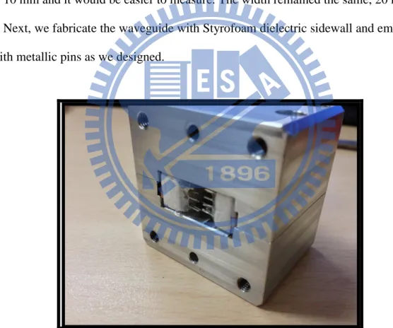
3-2 Final setting of dimesion – width: 20 mm & height:
10 mm ... 39 3-2-1 The pictures of the finished manufacture ... 39 3-2-2 The comparison of the S-parameter by simulated
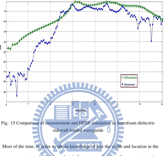
and measured ... 41 3-2-3 The CST simulation of the Styrofoam substrate ... 43 3-2-4 The comparison of the measurement and simulation
results of the Styrofoam substrate ... 44 CHAPTER 4 Conclusion ... 47 REFERENCE ... 48
x
LIST OF FIGURES
Figure 1 Lattice of grounded metallic pins, or bed-of-nails, embedded within a
slab of dielectric host ... 3
Figure 2 Transverse equivalent network of TE0N waveguide ... 5
Figure 3 Grounded dielectric substrate with thickness d and (µd, ɛd) material ... 5
Figure 4 Comparison of Matlab and CST simulation results ... 10
Figure 5 Geometry of partially dielectric-loaded rectangular waveguide ... 11
Figure 6 Cross-sectional view of a rectangular waveguide with dielectric sidewall loading embedded with a lattice of pins (a.k.a. bed-of-nails), (a). finite periodicity, and (b). infinitesimal period for asymptotic treatment ... 12
Figure 7 Perspective view of pin-lattices sidewall-loaded waveguide ... 12
Figure 8 Simulation results of the comparison of CST and HFSS ... 37
Figure 9 Simulation results of the comparison of MATLAB and HFSS ... 38
Figure 10 (a) Front sight of the sidewall-dielectric waveguide ... 39
(b) Side sight of the sidewall-dielectric waveguide ... 39
(c) The front sight of WR90 adaptor ... 40
(d) The waveguide connected with the adaptor ... 40
(e) The setting of the measurement ... 41
Figure 11 The comparison of the simulation and measurement ... 42
Figure 12 CST eigenmode simulation of RO-3010 substrate ... 42
Figure 13 The CST simulation of the Styrofoam material substrate embedded with sidewall pins... 43
Figure 14 Perspective view of rectangular waveguide with sidewall dielectric embedded within metallic pins ... 44 Figure 15 Comparison of measurement and HFSS simulation in Styrofoam
xi
- 1 - I. Introduction
Usually, the hollow waveguide can be manufactured in two parts that are joined together, but there would be a big problem which is that we cannot ensure good electrical contact in the joints. When it comes to radio frequency transmission, the micro-strip lines are commonly used as well, but the losses increase with frequency, as well as the power handling capability being reduced.
Therefore, there is a need for new waveguides or transmission lines operating at high frequencies, in particular above 30 GHz. There exist already some waveguides particularly intended for use at high frequencies. Such a waveguide is the so-called substrate integrated waveguide (SIW), as described in [6].
However, these waveguides still suffer from losses due to the substrate, and the metallized via holes represent a complication that is expensive to manufacture.
The first conceptual attempt to realize magnetic conductivity (in the form of high surface impedance) was the so-called soft and hard surfaces. For its abnormal characteristic which is the equivalent of magnetic conductivity, such materials are often referred to as meta-materials.
Recently, there has been a new type of novel meta-surfaces, which is called “pin-lattice” or “bed-of-nails”.[2] Its characteristics are similar to those of EBG (electromagnetic band-gap) structures, which are well-known for suppressing surface wave propagation in a specific band. [3][4]
The “bed-of-nails” structure can also be applied in the ridge gap waveguide.[7] The reason of this structure being used is because it can usually mimic the ideal impedance boundary. When we put a ridge in the parallel plate and surround it with an infinite array of periodic pins, and when the air gap is smaller than
- 2 -
quarter-wavelength, TEM waves propagate along the ridge.[1]
II. Theory
2-1 Modal Analysis of a Periodic Pins Array within a Grounded Dielectric Substrate
In this section, we analyze a basic structure being simply a grounded dielectric substrate and seek to demonstrate that by the concept of assuming TEM solution in the dielectric region perpendicular to the slab surface, the presence of the pin lattice within the dielectric slab can be effectively taken into account in an asymptotic manner. As in, the solution approaches exactness as the period of the lattice tends to zero. Besides, we demonstrated the characteristic equation with a key concept which is we assume the TEM solution within the dielectric region to the normal direction of the slab surface. That is to say, it will only be sense by the vertical y-oriented embedded pins in the substrate when TM modes. Which means the y TEymodes won’t feel them. Hence, we derive the equation only for y
TM modes.
In the next section, we use the classical analysis by vector potentials and we assume a “TEM-to-slab-surface-normal” solution inside the pin-lattice layer. In that way, the approach is reasonable only when the pin-period is diminishingly small, i.e. the density of the pins would be likely to infinity. As mentioned, we use the key concept, and let kd, the wavenumber in the dielectric, to equal kyd, the wavenumber
along the y-direction in the dielectric, perpendicular to the surface. The reason for this is because the wave within the space between adjacent pins was forced to propagate
- 3 -
along them, and acting as a transmission line, thereby tantamount to being TEM to the direction perpendicular to the slab surface.
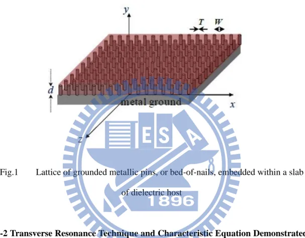
Figure 1 below shows the structure of the lattice of grounded metallic pins embedded within a slab of dielectric host.
Fig.1 Lattice of grounded metallic pins, or bed-of-nails, embedded within a slab of dielectric host
2-2 Transverse Resonance Technique and Characteristic Equation Demonstrated by Vector-potential Method
This section presents the derivation of the TM mode characteristic equation in the substrate without any pins embedded by using the vector-potential method. Next step, we then let kd = kyd. This turns out to be exactly the same as using the transverse
resonance technique (TRT).[5] Before commencing with the vector-potential method, we first introduce the TRT. Fig. 2 below shows the transverse equivalent network of the TE0N waveguide.
- 4 -
In the transverse resonance method the cross section of a traveling wave structure is represented as a transmission line network. The method can be illustrated with Fig.2, which shows a simple example with a conventional TE0N waveguide.
For this structure, a TE wave travels in the x direction with propagation constant γx,
and the Z0N represents the characteristic impedance of the transmission line. At any
point, when we look into the impedance line of the transverse network from the positive x direction would be equal and it would be opposite when we look into the negative x direction. This is the same applied to admittance. Which follows the continuity that the components of E and H are tangential to a plane orthogonal to the transverse transmission line, also means that x = constant plane in Fig.2.
Another way to state the impedance relationship is that the sum of the two impedances that are observed by opposite directions from a point on the line must be canceled to zero.
From the above discussion it is clear that one needs to know both the impedance of the equivalent line and the aperture impedance in order to apply transverse resonance.
Transverse resonance technique is a method to find the propagation constant of many practical traveling wave structures.
- 5 -
Fig.2 Transverse equivalent network of TE0N waveguide
After briefly introducing the TRT, the vector-potential method is discussed. Fig.3 below shows the grounded dielectric substrate with thickness d and (µd, ɛd) material. It
is along the x-z plane, and y-axis is the normal direction.
- 6 -
The various field components of theTM modes are stated as follow. [7] y
2 1 y x A E j x y ; 2 2 1 y y E k A j y ; 2 1 y z A E j y z (a1) 1 y x A H z ; Hy 0; 1 y z A H x (a2)
For the slab region: script “d”: 0 y d
d y( , 0 , ) | 0 | 0 xd xd jk x jk x d d x x x x A x y d z C e D e 0 0 cos( ) sin( ) jk zzd | jk zzd | d d d d y yd y yd z z z z C k y D k y C e D e (Eq-1)
For the upper (air) region: script “0”: y d
0 0 0 0 0 0 0 ( , , ) jkx x| jkx x| y x x x x A x yd z C e D e 0( ) 0 0 0 0 0 0 | | y z z jk y d jk z jk z z z x z e C e D e (Eq-2)
The boundary conditions are stated as follow.
( , 0, ) 0 d x E x y z (BC-1a) ( , 0, ) 0 d z E x y z (BC-1b) 0 ( , , ) ( , , ) d x x E x yd z E x yd z (BC-2a) 0 ( , , ) ( , , ) d z z E x yd z E x yd z (BC-2b) 0 ( , , ) ( , , ) d x x H x yd z H x yd z (BC-3a)
- 7 - 0 ( , , ) ( , , ) d z z H x yd z H x yd z (BC-3b)
By (a1), (a2), (Eq-1), and (Eq-2), we can state these equations of each region as below:
2 0 0 1 | | xd xd d y xd yd jk x jk x d d d x x x x x d d d d A jk k E D e C e j x y j cos( ) sin( ) jk zzd jk zzd d d d d y yd y yd z z zero D k y C k y C e D e (Eq-3)
Then applying (BC-1a): we getDdy 0.
Next, 2 0 0 1 | | xd xd d y zd yd jk x jk x d d d z x x x x d d d d A jk k E C e D e j y z j cos( ) sin( ) jk zzd jk zzd d d d d y yd y yd z z zero D k y C k y D e C e (Eq-4) Next, 0 0 2 0 0 0 0 0 0 0 0 0 0 0 0 ( ) 1 | | x x y x y jk x jk x x x x x x A jk jk E D e C e j x y j 0( ) 0 0 0 0 y z z jk y d jk z jk z z z e C e D e (Eq-5) Then, applying (BC-2a):
0 0 | | sin( ) xd xd zd zd zd yd d jk x d jk x d d jk z d jk z x x x x y yd z z d d k k D e C e C k d C e D e 0 0 0 0 0 0 0 0 0 0 0 0 0 0 ( ) | | x x z z x y jk x jk x jk z jk z x x x x z z k k D e C e C e D e j (Eq-6) Next, 0 0 2 0 0 0 0 0 0 0 0 0 0 1 | | x x y y z jk x jk x z x x x x d d A jk jk E C e D e j y z j
- 8 - 0( ) 0 0 0 0 y z z jk y d jk z jk z z z e D e C e (Eq-7) Then, applying (BC-2b): 0 0 | | sin( ) xd xd zd zd zd yd d jk x d jk x d d jk z d jk z x x x x y yd z z d d k k C e D e C k d D e C e 0 0 0 0 0 0 0 0 0 0 0 0 0 0 | | x x z z y z jk x jk x jk z jk z x x x x z z k k C e D e D e C e j (Eq-8)
Next, need H and x H in both layers:z
0 0 1 | | cos( ) xd xd zd zd d y jk x jk x jk z jk d d zd d d d d d x x x x x y yd z z d d A jk H C e D e C k y C e D e z (Eq-9) 0 0 0 0 0 0 ( ) 0 0 0 0 0 0 0 0 0 0 1 | | y x x jk y d z z y z jk x jk x jk z jk z x x x x x z z A jk H C e D e e C e D e z (Eq-10) 0 0 0 0 0 0 ( ) 0 0 0 0 0 0 0 0 0 0 1 | | y x x jk y d z z y x jk x jk x jk z jk z z x x x x z z A jk H D e C e e C e D e x (Eq-11) Then applying (BC-3a):
0 0 | | cos( ) xd xd zd zd jk x jk x jk z jk z d d d d d zd x x x x y yd z z d k C e D e C k d C e D e 0 0 0 0 0 0 0 0 0 0 0 0 | | x x z z jk x jk x jk z jk z z x x x x z z k C e D e C e D e (Eq-12) And applying (BC-3b): 0 0 | | cos( ) xd xd zd zd jk x jk x jk z jk z d d d d d xd x x x x y yd z z d k D e C e C k d C e D e 0 0 0 0 0 0 0 0 0 0 0 0 | | x x z z jk x jk x jk z jk z x x x x x z z k D e C e C e D e (Eq-13) Dividing (Eq-6) by (Eq-13):
- 9 - 0 0 tan( ) yd y yd d k k k d j (Eq-14) Then we setky0 jy0,
Here, we only consider the slow wave, so we think about the “–ja” situation only, and then we will get:
0 0 tan( ) yd y yd d k k d (Eq-15)
Next, we let kyd kd d d [9], and the above equation becomes:
0 0 tan( ) y d d d k k d 0 0 00 tan( ) tan( ) tan( )
d d d y d d d d d d d k k k k d k d k d (Eq-16)
By dividing (Eq-8) by (Eq-12) above, we can obtain the exact same equation.
However, we still need one more correction factor for the real case which the metallic-pins aren’t being infinite.
It is fairly presumed that the electric fields on the substrate surface may be corrected by an incremental factor w/(w + t), where w is the distance between two pins, and t is the diameter of the pin, yielding
0 0 tan( ) d y d d k w k d w t (Eq-17) 2-3 Simulation result
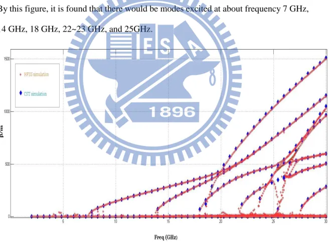
We get the characteristic equation above, and then use the simulate tools CST and Matlab to observe their agreement. Fig.4 below shows the simulation result. The blue
- 10 -
square would be the Matlab result, and the purple star represents the CST result. We can find out that they have excellent agreement in every mode.
Fig.4 Comparison of Matlab and CST simulation results
By this result, we can prove that our vector-potential method matches to the TRT (Transverse Resonance Technique) solution.
2-4 Rigorous analysis of partially dielectric-loaded rectangular waveguide using vector potential method
Here, we will demonstrate treatment methods of inhomogeneously dielectric-loaded rectangular waveguide.
2-4-1 Analytical Modal Field Solutions
- 11 -
empty rectangular waveguide with two E-plane sidewalls (when fundamental modal electric field is parallel to these side walls) which are coated with a dielectric lining of a certain thickness 4 1 TEM r d , where TEM TEM c f
, with fTEM being the designated TEM frequency.
The geometry of the structure is shown in the figure below.
Fig.5 Geometry of partially dielectric-loaded rectangular waveguide
Fig.6 (a) and (b) below shows the cross-sectional view of rectangular waveguide with dielectric sidewall loading embedded with a lattice of pins.
Fig.7 below represents the perspective view of pin-lattice sidewall-loaded waveguide.
- 12 -
Fig.6 Cross-sectional view of a rectangular waveguide with dielectric sidewall loading embedded with a lattice of pins (a.k.a. bed-of-nails), (a). finite periodicity, and
(b). infinitesimal period for asymptotic treatment.
- 13 -
The modal fields within this inhomogeneously-filled waveguide are neither TEz
norTM , but rather are mode configurations that are combinations of these two modes. z
Such combined modes are referred to as hybrid modes or longitudinal section electric (LSE) or longitudinal section magnetic (LSM) modes.
2-4-2 Case (I): LSEx or TEx mode (for above geometry, with x normal to
discontinuity interface)
(A) For central freespace region: a x a: subscript ‘0’
-0 0 0 0 0 0
0 0 0 0
(- , , ) cos sin cos sin zz
x x x x x y y y y z
F a x a y z C k x D k x C k y D k y A e
(IA1) with
z z jkz
(IA2a) which is valid throughout
and
2 2 2 2 2
0 0 0 0 0
x y z
k k k (IA2bi) for generally lossy case
2 2 2 2 2
0 0 0 0 0
x y z
k k k k (IA2bii) for lossless case with z 0
(B)For dielectric region: (a d) x a and a x a d
(1)Left dielectric region: (a d) x a (superscript or subscript ‘1’)
1 1 (1) 1 (1) [ ( ) , , ] cos ( ) sin ( ) d d d x x xd x xd F a d x a y z C k x a d D k x a d
1 (1) 1 (1)
1 cos sin zz d d d y yd y yd z C k y D k y A e (IB1a)- 14 - with 2 2 (1) (1) 2 2 2 xd yd z d d d k k k
(IB1bi) for generally lossy case
2 2
(1) (1) 2 2 2
xd yd z d d d
k k k k
(IB1bii) for lossless case withz 0 (2)Right dielectric region: a x a d (superscript or subscript ‘2’)
2 2 (2) 2 (2) [ , , ] cos ( ) sin ( ) d d d x x xd x xd F a x a d y z C k x a d D k x a d
2 (2) 2 (2)
2 cos sin zz d d d y yd y yd z C k y D k y A e (IB2a) with 2 2 (2) (2) 2 2 2 xd yd z d d d k k k (IB2bi) for generally lossy case and 2 2 (2) (2) 2 2 2 xd yd z d d d k k k k
(IB2bii) for lossless case with z 0
(C)Boundary Conditions: (1) Ezd1
x (a d), 0 y h z,
Ezd2
x a d, 0 y h z,
0 (IC1) (2a) Ezd1
x (a d) x a y, 0,z
Ezd1
x (a d) x a y, h z,
0 (IC2a) (2b) Ezd2
a x a d y, 0,z
Ezd2
a x a d y, h z,
0 (IC2b) (3) Ez0
a x a y, 0,z
Ez0
a x a y, h z,
0 (IC3) (4a) Ezd1
x a, 0 y h z,
Ez0
x a, 0 y h z,
(IC4a) (4b) Ezd2
xa, 0 y h z,
Ez0
xa, 0 y h z,
(IC4b) (5a) Hzd1
x a, 0 y h z,
Hz0
x a, 0 y h z,
(IC5a)- 15 - (5b) Hzd2
xa, 0 y h z,
Hz0
xa, 0 y h z,
(IC5b) (6) Eyd1
x (a d), 0 y h z,
Eyd2
x a d, 0 y h z,
0 (IC6) (7a) Exd1
(a d) x a y, 0,z
Exd1
(a d) x a y, h z,
0 (IC7a) (7b) Exd2
a x a d y, 0,z
Exd2
a x a d y, h z,
0 (IC7b) (8) Ex0
a x a y, 0,z
Ex0
a x a y, h z,
0 (IC8) (9a) Edy1
x a, 0 y h z,
Ey0
x a, 0 y h z,
(IC9a) (9b) Edy2
xa, 0 y h z,
Ey0
xa, 0 y h z,
(IC9b) (10a) Hyd1
x a, 0 y h z,
Hy0
x a, 0 y h z,
(IC10a) (10b) Hyd2
xa, 0 y h z,
Hy0
xa, 0 y h z,
(IC10b) For LSEx mode, we know that1 x z F E y Therefore, we have: Using (IA1): 0 0 0 0 0 0 0 0 0 0 0 0 0 0 1
cos( ) sin( ) cos( ) sin( ) z
y z x z x x x x y y y y z k F E C k x D k x D k y C k y A e y Apply (IC3):
0 0 , 0, 0 0 z y E a x a y z D
0 0 , , 0 z y n E a x a y h z k h Thus 0 0 0 0 0 0 0 0 0 0cos( ) sin( ) sin( ) z
y z z x x x x y y z k E C k x D k x C k y A e (I1)
- 16 - Using (IB1): 1 1 1 d d x z d F E y
(1) 1 (1) 1 (1) cos ( ) sin ( ) yd d d x xd x xd d k C k x a d D k x a d
1 (1) 1 (1)
1 cos sin zz d d d y yd y yd z D k y C k y A e Apply (IC1): Ezd1
x (a d)
0 Cxd10 Apply (IC2a): 1 1 1 (1) ( 0) 0 0 ( ) 0 d d z y d z yd E y D n E y h k h Thus
(1) 1 1 (1) 1 (1) 1 sin ( ) sin z yd z d d d d z x xd y yd z d k E D k x a d C k y A e (I2) Using (IB2): 2 2 1 d d x z d F E y
(2) 2 (2) 2 (2) cos ( ) sin ( ) yd d d x xd x xd d k C k x a d D k x a d
2 (2) 2 (2)
2 cos sin zz d d d y yd y yd z D k y C k y A e Apply (IC1): Ezd2
x a d
0 Cxd2 0 Apply (IC2b): 2 2 2 (2) ( 0) 0 0 ( ) 0 d d z y d z yd E y D n E y h k h Thus
(2) 2 2 (2) 2 (2) 2 sin ( ) sin z yd z d d d d z x xd y yd z d k E D k x a d C k y A e (I3)- 17 - Use (I1) and (I2) in (IC4a):
0 0 0 0 0 0 0 0 0 (1) 1 (1) 1 (1) 1cos( ) sin( ) sin( )
sin sin z z y z x x x x y y z yd d d d z x xd y yd z d k C k a D k a C k y A e k D k d C k y A e Since ky0 k(1)yd n h , thus 0 0 1 1 1 0 0 (1) 0 0 0
cos( ) sin( ) sin
d d d y z x y z x x x x xd d C A D C A C k a D k a k d (I4)
Use (I1) and (I3) in (IC4b):
0 0 0 0 0 0 0 0 0 (2) 2 (2) 2 (2) 2cos( ) sin( ) sin( )
sin sin z z y z x x x x y y z yd d d d z x xd y xd z d k C k a D k a C k y A e k D k d C k y A e Since ky0 k(2)yd n h , thus 0 0 2 2 2 0 0 (2) 0 0 0
cos( ) sin( ) sin
d d d y z x y z x x x x xd d C A D C A C k a D k a k d (I5) Also for LSEX modes,
2 1 x z F H j x z
Hence using (IA1), whose D0y 0:
2 0
0 0 0 0 0 0
0 0 0
0 0 0 0
1
cos( ) sin( ) cos( ) zz
x x z z x x x x y y z F k H D k x C k x C k y A e j x z j (I6)
Using (IB1) with its Cxd1Dyd10
2 1 (1) 1 1 1 (1) 1 (1) 1 cos ( ) cos z d z d x xd z d d d z x xd y yd z d d d d F k H D k x a d C k y A e j x z j (I7)- 18 -
2 2 (2) 2 1 2 (2) 2 (2) 2 cos ( ) cos z d z d x xd z d d d z x xd y yd z d d d d F k H D k x a d C k y A e j x z j (I8) Use (I6) and (I7) in (IC5a):
0 0 0 0 0 0 0 0 0 0 (1) 1 (1) 1 (1) 1sin( ) cos( ) cos( )
cos cos z z z x z x x x x y y z z d d d xd z x xd y yd z d d k C k a D k a C k y A e j k D k d C k y A e j Again with ky0 kyd(1) n h , (1) 1 1 1 0 0 0 0 (1) 0 0 0 0 0
sin( ) cos( ) cos
d d d xd x y z x x x x x y z xd d d k D C A k C k a D k a C A k d (I9)
Use (I6) and (I8) in (IC5b):
0 0 0 0 0 0 0 0 0 0 (2) 2 (2) 2 (2) 2cos( ) sin( ) cos( )
cos cos z z z x z x x x x y y z z d d d xd z x xd y yd z d d k D k a C k a C k y A e j k D k d C k y A e j Again with ky0 kyd(2) n h , (2) 2 2 2 0 0 0 0 (2) 0 0 0 0 0
cos( ) sin( ) cos
d d d xd x y z x x x x x y z xd d d k D C A k D k a C k a C A k d (I10)
Divide (I4) by (I9), we have
0 0 (1)
0 0 0
(1)
0 0
0 0 0
cos( ) sin( ) tan
sin( ) cos( ) x x x x d xd xd x x x x x C k a D k a k d k k C k a D k a (I11)
Divide (I5) by (I10), we have
0 0 (2)
0 0 0
(2)
0 0
0 0 0
cos( ) sin( ) tan
sin( ) cos( ) x x x x d xd xd x x x x x C k a D k a k d k k C k a D k a (I12)
- 19 - 1 x y F E z and 2 1 x y F H j x y
Thus, using (IB1) with its Cxd1Dyd10, we have
1 1 1 1 (1) sin ( ) d d x z d y x xd d d F E D k x a d z
1 (1)
1 cos zz d d y yd z C k A e (I13) 2 1 1 1 d d x y d d F H j x y
(1) (1) 1 (1) 1 (1) 1 cos ( ) sin z xd yd d d d z x xd y yd z d d k k D k x a d C k y A e j (I14) Apply (IB2) with its Cxd2 Dyd2 0,
2 2 1 2 (2) sin ( ) d d x z d y x xd d d F E D k x a d z
d2c o s ( 2 )
d 2 zz y yd z C k A e (I15) 2 2 2 1 d d x y d d F H j x y
( 2 ) ( 2 ) 2 ( 2 ) 2 ( 2 ) 2 c o s ( ) s i n z x d y d d d d z x x d y y d z d d k k D k x a d C k y A e j (I16) Apply (IA1) whose D0y 0,0
0 0 0 0 0
0 0 0
0 0
1
cos( ) sin( ) cos( ) zz
x z y x x x x y y z F E C k x D k x C k y A e z (I17) 0 0 0 0 1 x y F H j x y 0 0 0 0 0 0 0 0 0 0 0
cos( ) sin( ) sin( ) z
x y z x x x x y y z k k D k x C k x C k y A e j (I18)
2-4-2.1 Case One: Symmetric Even LSEx Mode i.e. 0
0
x
- 20 - With 0
0
x
D , equation (I11) yields:
(1) 0 0 (1) 0 0 tan cos( ) sin( ) d xd x x x xd k d k a k k a k
Equivalently, upon inverting:
(1) (1) 0 0 0 tan( ) cot x xd x xd d k k k a k d (I-ES1) where 2 2 2 2 2 2 0 0 0 0 0 0 x y z y z
k k k k which is from (IA2bi) for generally lossy
case
and kx0 k02ky20kz2 2 0 0ky20kz2 which is from (IA2bii) for lossless case
also (1) (2) 2 (1) 2 2 2 (2) 2 2 2 2 2
0
xd xd d yd z d yd z d d y z
k k k k k k k
which is from (IB1bi) for generally lossy case,
and kxd(1)kxd(2) kd2kyd(1)2kz2 2 d d ky20kz2
which is from (IB1bii) for lossless case
where ky0 k(1)yd k(2)yd n h
Therefore, for a certain frequency
(2 )
f , and for a particular nth mode (corresponding to y0 yd(1) (2)yd
n
k k k
h
and a certainzn ), the above dispersion equation (I-ES1) may be explicitly expressed as:
2 2 2 2 0 0 2 2 0 0 0 tan zn zn n h n a h 2 2 2 2 2 2 cot d d zn d d zn d n h n d h (I-ES2)
- 21 - whose only unknown is zn, [for a certain n
th
mode and at a specific frequency
(2 )
f ], which can then be solved for numerically.
This solvedzn, together with ky0 n h
, can then be substituted into above equations
for k to obtain xd k and x0 kxd(1) kxd(2).
It is noted that dmay be expressed asd rdcomplex0, withrdcomplex rd jrd"
With 0
0
x
D , equation (I12) yields
(2) 0 0 (2) 0 0 tan cos sin d xd x x x xd k d k a k k a k d Equivalently, upon inverting:
(2) (2) 0 0 0 tan cot x xd x xd d k k k a k d (I-ES3)
Which is the same as (I-ES1) sincekxd(1)kxd(2).
Therefore, (I12) also will result in the same dispersion characteristic equation as does (I11).
From (I4), with 0
0 x D , we have:
0 0 0 1 1 1 (1) 0 0 cos sin d d d x y z x y z x xd d C C A D C A k a k d i.e.
1 1 1 0 0 0 0 (1) 0 cos sin d d d x y z d x x y z xd D C A k a C C A k d (I-ES4) Normalizing by setting 0 0 0 1 x y z C C A (I-ES5) Then (I-ES4) becomes
0
1 1 1 (1) 0 cos sin d x d d d x y z xd k a D C A k d (I-ES6)- 22 - Also from (I5), with 0
0 x D , we have
0 0 0 2 2 2 (2) 0 0 cos sin d d d x y z x y z x xd d C C A D C A k a k d i.e.
2 2 2 0 0 0 0 (2) 0 cos sin d d d x y z d x x y z xd D C A k a C C A k d (I-ES7) with kxd(1)kxd(2)As above, normalizing with (I-ES5), then (I-ES7) becomes:
0
2 2 2 (2) 0 cos sin d x d d d x y z xd k a D C A k d (I-ES8)Subsequently, using (I-ES5), (I-ES6) and (I-ES8), we can write expressions for all the electric and magnetic fields for this even symmetric LSEx mode (with 0
0
x
D ) using equations (I1) through (I18). It is stressed that these field expressions pertain to one
particular n mode corresponding to th (1) (2) 0 y yd yd n k k k h and a certain zn, at a specific frequency 2 f
. For each n root th zn obtained from the dispersion equation (I-ES2), there corresponds to a certain set of phase constants, namely:
(1) (2) 0 y yd yd n k k k h 2 2 2 0 0 0 0 x y zn k k 2 2 (1) (2) 2 (1) 2 2 (2) 2 2 2 2 0 xd xd d yd zn d yd zn d d y zn k k k k k k k From (I1):
0 0 0 0 0 cos sin zn y z z x y k E k x k y e (I-ES9) From (I17):- 23 -
0 0 0 0 cos sin zz z y x y E k x k y e (I-ES10) and 0 0 xE (since LSEx mode) (I-ES11) From (I6):
0 0 0 0 0 0 sin cos zz x z z x y k H k x k y e j (I-ES12) From (I18):
0 0 0 0 0 0 0 sin sin zn x y z y x y k k H k x k y e j (I-ES13) Now, for LSEx modes, we know that2 2 2 0 0 1 x x H k F j x
Then using (IA1) with Dy0 0as well,
2 0 2 0 2 2 0 0 0 0 0 2 0 0 0 0 1 1 cos cos znz x x x x y H k F k k k x k y e j x j (I-ES14) From (I2):
(1) 0 1 (1) (1) (1) 0 cos sin ( ) sin sin zn yd d x z d z xd yd d xd k k a E k x a d k y e k d (I-ES15) From (I13):
0
1 (1) (1) (1) 0 cos sin ( ) cos sin znz d x d zn y xd yd d xd k a E k x a d k y e k d (I-ES16) and 1 0 d xE (since LSEx mode) (I-ES17) From (I7):
(1) 0 1 (1) (1) (1) 0 cos cos ( ) cos sin znz d x d xd z z xd yd d d xd k a k H k x a d k y e j k d (I-ES18)- 24 - From (I14):
(1) (1) 0 1 (1) (1) (1) 0 cos cos ( ) sin sin zn xd yd d x z d y xd yd d d xd k k k a H k x a d k y e j k d (I-ES19)Using (IB1a), with its Cxd1 Dyd10, we have
2 1 2 1 2 2 2 (1) (1) (1) 0 (1) 0 1 cos( ) sin ( ) cos sin zn d d x d x d d d xd d x z xd yd d d xd H k F j x k k k a k x a d k y e j k (I-ES20) From (I3):
(2) 0 2 (2) (2) (2) 0 (2) 0 (2) (2) (2) 0 cos sin ( ) sin sin cos sin ( ) sin sin zn zn yd d x z d z xd yd d xd yd x z xd yd xd k k a E k x a d k y e k d k k a k x a d k y e k d (I-ES21) From (I15):
0 2 (2) (2) (2) 0 0 (2) (2) (2) 0 cos sin ( ) cos sin cos sin ( ) cos sin zn zn z d x d z y xd yd d xd z z x xd yd xd k a E k x a d k y e k d k a k x a d k y e k d (I-ES22) and 2 0 d xE (since LSEx mode) (I-ES23) From (I8):