國
立
交
通
大
學
電機與控制工程學系
碩
士
論
文
全電流控制高頻切換直流轉直流降壓式電源轉換器
High Switching DC-DC Buck Converters in Current Domain
Control
研 究 生:謝維倫
指導教授:陳科宏 博士
全電流控制高頻切換直流轉直流降壓式電源轉換器
High Switching DC-DC Buck Converters in Current Domain Control
研 究 生:謝維倫 Student:Wei-Lun Hsieh
指導教授:陳科宏 Advisor:Ke-Horng Chen
國 立 交 通 大 學
電 機 控 制 工 程 學 系
碩 士 論 文
A Thesis
Submitted to Department of Electrical and Control Engineering
College of Electrical Engineering
National Chiao Tung University
in partial Fulfillment of the Requirements
for the Degree of
Master
in
Electrical and Control Engineering
September 2008
Hsinchu, Taiwan, Republic of China
全電流控制高頻切換直流轉直流降壓式電源轉換器
研究生:謝維倫
指導教授:陳科宏博士
國立交通大學電機與控制工程研究所碩士班
摘 要
在可攜式電子產品的應用上,高效能和小型的電壓轉換器在提供系統
電源上扮演非常重要的角色。為了減少輸出級濾波器的面積,提出高頻切
換的直流轉直流降壓轉換器來達到元件整合的功能。然而,對傳統電流控
制模式之直流轉直流降壓轉換器來說並不適合在高頻切換的操作,因為使
用到運算放大器之子電路其頻寬會被限制住。也就是說,由於電路頻寬的
極限造成不正確的操作且無法跟上系統的操作頻率。為了保證電壓轉換器
可以操作在高切換頻率下,全電流脈波寬度調變控制器在本論文中被提出
了。
由於使用了全電流脈波寬度調變控制器,因為少了外部補償元件使得
操作電路將會變的較簡單,且控制訊號全都轉換成電流形式讓訊號相加變
得直接。為了能提供高效能電源電壓,也是其中一種電流模式控制技術的
全電流脈波寬度調變控制器將可得到較佳的線調節率和負載調節率。
本篇論文實現了 20MHz 的全電流控制高頻切換直流轉直流降壓式電源
轉換器,且以台灣積體電路製造股份有限公司點三五微米互補式金氧製程
來實現,輸入電壓範圍從 3.0 伏特到 4.0 伏特,其負載調節率及線調節率分
別為 0.18356mV/mA 和 48.5V/V。系統特色為可使用較小的外部濾波元件且
得到較快的暫態響應,其中電感大小只需 200nH、輸出電容值只需 5µF。非
常適合於可攜式電子產品之電源管理。
High Switching DC-DC Buck Converters in Current Domain Control
Student: Wei-Lun Hsieh
Advisor: Dr. Ke-Horng Chen
Department of Electrical and Control Engineering
National Chiao-Tung University
Abstract
For portable electronic device applications, high performance and compact size voltage regulator plays an important role to provide system power. To reduce the size of output filter, a high switching dc-dc buck converter is presented to achieve high integration. However, the conventional current mode DC-DC buck converter is not suitable to high switching design because the sub-circuits, which uses operational amplifier, restrict the bandwidth. That is to say, the limitation of circuit bandwidth causes incorrect operation and can not follow the system switching frequency. To ensure the switching regulator can operate at high switching frequency, the current domain PWM controller is presented in this thesis.
Owing the current domain PWM controller, the circuit implementation becomes simple and there are not any external compensation components. The control signals are transformed to current form to process addition of control signal directly. For providing a high performance supply voltage, the current domain PWM control is one of current-mode technique to get good line and load regulations.
In this thesis, a high switching DC-DC buck converter in current domain control with frequency 20MHz is implemented. The test chip was implemented by TSMC 2P4M 0.25-µm CMOS technology. Input operation range varies from 3.0V to 4.0V. The load regulation and line regulation are 0.18356mV/mA and 48.5mV/V respectively. The system features smaller output filter. That is, the inductor and output capacitor values are only 200nH and 5μF respectively. Fast transition response is achieved and demonstrates the design suitable for power management in the portable devices.
誌 謝
能夠完成此篇論文,首先一定要向我的指導教授 陳科宏博士致上萬分的謝意,感 謝老師這兩年來無論是專業知識或是做人處事上的指導,讓我的研究生生涯學習到獨立 思考的精神以及解決問題的能力。更慶幸當年研究所放榜尋找指導教授時,老師不介意 當時沒有相關研究背景的我,讓我有這個機會加入混合信號與電源管理晶片設計實驗 室,展開另一段充實的研究時光。老師這兩年的指導,足以讓學生感念一輩子,謝謝老 師。 能夠在實驗室得到許多的知識,首先要感謝畢業的學長姐不吝嗇的指導,更感謝博 士班學長宏瑋、契霖在研究上細心的教導。感謝國林、小柯、逢哥在晶片佈局技術上給 予我相當多的支援。特別要謝謝我的同袍戰友俊禹、家祥、佳麟、鼎容、韋任,與你們 一起學習、歡笑、成長的時光,是我這兩年最精采的回憶。最後要謝謝701、703以及802 實驗室的學長、學弟妹們這兩年的協助。 要感謝我的父母、我的女朋友明娟以及其他在背後支持著我的好友們,因為有你們 的扶持我才能順利的完成碩士學業。最後僅以一句話代表我感謝的心意:要謝的人太多 了,那就謝天吧!Contents
Chapter 1 ...1
Introduction ...1
1.1 Background of Power Management System ...1
1.2 Classification of Voltage Regulators ...3
1.2.1 Linear Regulator ...3 1.2.2 Charge Pump ...5 1.2.3 Switching Regulator ...6 1.2.4 Comparison...7 1.3 Motivation ...8 1.4 Thesis Organization ...9 Chapter 2 ...10
Basic Knowledge of Switching Regulator...10
2.1 Topologies of DC-DC Converter...10
2.2 Technologies of Controlling Modulator ...12
2.2.1 Pulse Width Modulation (PWM)...13
2.2.2 Pulse Frequency Modulation (PFM) ...14
2.2.3 Hysteretic Control technique ...16
2.3 The Theorem of Current Mode Control...18
2.3.1 Operation Principles of Current Mode Buck Switching Regulator...19
2.3.2 Sub-harmonic Oscillation at Duty Ratio > 0.5 ...21
2.3.3 Ramp Compensation ...23
2.3.4 Continuous Conduction Mode (CCM) and Small Signal Modeling ...25
2.3.5 Discontinuous Conduction Mode (DCM) and Small Signal Modeling ...30
2.4 Important Specifications of Switching Converter ...35
2.4.1 Efficiency...35
2.4.2 Load and Line Regulation ...36
2.4.3 Transient Response ...37
Chapter 3 ...39
Structure of 20MHz Current Domain DC-DC Buck Converter ...39
3.1 Proposed Current Domain 20MHz Buck Converter...39
3.1.1 Prior Art Conventional Current Mode Buck Converter ...39
3.1.2 Current Domain 20MHz Buck Converter ...41
3.2 Small Signal Analysis and Compensation Scheme of Current Domain DC-DC Buck Converter ...42
3.2.1 Small Signal Analysis [5] ...42
3.2.2 Structure of PI-Compensator ...48
3.2.3 P-Compensator ...50
3.3 Soft Start Technique ...51
3.4 Output Inductor and Capacitor Selection ...53
Chapter 4 ...55
Circuit Implementation and Simulation Results...55
4.1 P-Compensator ...55
4.2 Current Sensing Circuit ...59
4.3 Ramp Generator...63
4.4 Clock Generator...65
4.5 Current Comparator...71
4.6 Soft Start ...73
Chapter5 ...75
System of High Switching DC-DC Buck Converter in Current Domain Control Simulation Results, Conclusions and Future Work...75
5.1 System Simulation Results ...75
5.1.1 Start Up...75
5.1.2 Steady State of Output Voltage ...77
5.1.3 Load Regulation ...78
5.1.4 Line Regulation ...78
5.1.5 Efficiency...79
5.1.6 Performance and Specification...80
5.2 Conclusions ...81
5.3 Future Work ...82
Figure Captions
Fig. 1. Energy constrained operation...2
Fig. 2. Power management system diagram of cell phone.[1] ...3
Fig. 3. The basic structure of linear regulator...4
Fig. 4. The basic structure of charge pump. ...5
Fig. 5. The basic structure of buck type voltage mode switching regulator. ...7
Fig. 6. Three basic topologies of DC-DC converter. ... 11
Fig. 7. Pulse-width modulation waveform. ...14
Fig. 8. Analysis of conduction loss and switching loss at Pulse-width modulation ...14
Fig. 9. Pulse-frequency modulation waveform. ...15
Fig. 10. Analysis of conduction loss and switching loss at Pulse frequency modulation ...16
Fig. 11. The block diagram of Hysteretic control technique ...17
Fig. 12. The conventional current-mode buck converter...18
Fig. 13. The function blocks of the current-mode DC-DC buck converter...20
Fig. 14. Steady-state and perturbed Inductor Current Waveform...21
Fig. 15. The stable situation and unstable oscillation of inductor current...22
Fig. 16. Current-mode control signal with the compensation ramp and inductor current...23
Fig. 17. Steady-state and perturbed inductor current waveforms with ramp compensation. ...25
Fig. 18. The inductor and output current operates in continuous conduction mode. ...26
Fig. 19. The operating states in continuous conduction mode. ...26
Fig. 20. The small signal ac equivalent circuit model of CCM condition... 29
Fig. 21. The inductor and output current operates in discontinuous conduction mode...30
Fig. 22. The third subinterval of discontinuous conduction mode. ...31
Fig. 23. Definition of terminal quantities of the buck switch network...33
Fig. 24. The small signal ac equivalent circuit model of DCM condition. ...34
Fig. 25. The transient response of output voltage relates to load current...38
Fig. 26. The structure of conventional current mode DC-DC buck converter. ...40
Fig. 27. The structure of modified current domain 20MHz buck converter...42
Fig. 28.The relationship between sensing inductor current ics(t)and control current ic(t). ...43
Fig. 29. Small signal model of current domain dc-dc buck converter...45
Fig. 31. The block diagram of the feedback system with current mode control. ...48
Fig. 32. Schematic of PI-compensator...48
Fig. 33. The Bode plot of PI-compensator...50
Fig. 34.Schematic of P-compensator. ...51
Fig. 35. The inrush current without soft start technique...52
Fig. 36. The simply soft start diagram...53
Fig. 37. Schematic of the P-Compensator. ...56
Fig. 38. Schematic of different P-Compensator input stages. (a) Voltage follower. (b) Folded voltage follower. (c) Folded flipped voltage follower. ...58
Fig. 39. The simulation result of P-Compensator...58
Fig. 40. Schematic of the current sensing circuit ...60
Fig. 41. The simulation results of current sensing circuit with Heavy load condition...61
Fig. 42. The simulation results of current sensing circuit with Light load condition...62
Fig. 43.Schematic of the ramp generator circuit [14]...63
Fig. 44. The simulation result of ramp generator circuit ...65
Fig. 45. Schematic of the clock generator circuit. ...66
Fig. 46. Schematic of the one shot circuit. ...67
Fig. 47. The additional logic with S-R latch...68
Fig. 48. Schematic of the voltage comparator. ...69
Fig. 49. The simulation results of voltage comparator. ...70
Fig. 50. The simulation results of clock generator. ...70
Fig. 51. Schematic of the current comparator circuit ...72
Fig. 52. Simulation results of the current comparator circuit...73
Fig. 53. Schematic of the soft start circuit ...74
Fig. 54. The start up response waveform without soft start circuit.(@ VIN=3.3V, Iload=50mA) ...76
Fig. 55. The start up response waveform with soft start circuit.(@ VIN=3.3V, Iload=250mA)..76
Fig. 56. The steady state output voltage and inductor current waveform. (@ VIN=3.3V, Iload=50mA)...77
Fig. 57. The load regulation waveform (@ VIN=3.3V). ...78
Table Captions
TABLE I. COMPARISONS OF DIFFERENT TYPE REGULATORS. ...8
TABLE II. COMPARISONS OF CONVERTER TOPOLOGIES...12
TABLE III. COMPARISONS BETWEEN PWM AND PFM CONTROL...36
TABLE IV. THE SIMULATION CONDITIONS...55
TABLE V. THE LINEARITY BETWEEN IDEAL AND ACTUAL TRANSCONDUCTANCE...59
TABLE VI. SENSING ACCURACY IN DIFFERENT LOAD CONDITIONS...62
TABLE VII. THE TRUTH TABLE OF THE S-RLATCH WITH ADDITIONAL LOGIC...68
TABLE VIII. THE CLOCK GENERATOR OPERATING FREQUENCY IN DIFFERENT CONDITIONS...71
Chapter 1
Introduction
In recent years, power management has become more popular and important subject because the electronic devices need longer usage lifetime, especially for battery-based portable devices such as personal digital assistance (PDA), cell phone and digital camera (DCS). That is to say, effective energy usage and minimum power loss are two major topics to achieve power consumption efficiency enhancement. In this chapter, we will show the background and basic knowledge of power management system in chapter 1.1 firstly. The classification of power management circuits which including switching converters, linear regulators, and charge pump converters will show in chapter 1.2. The motivation will give in chapter 1.3. Finally, the thesis organization will show in chapter 1.4.
1.1 Background of Power Management System
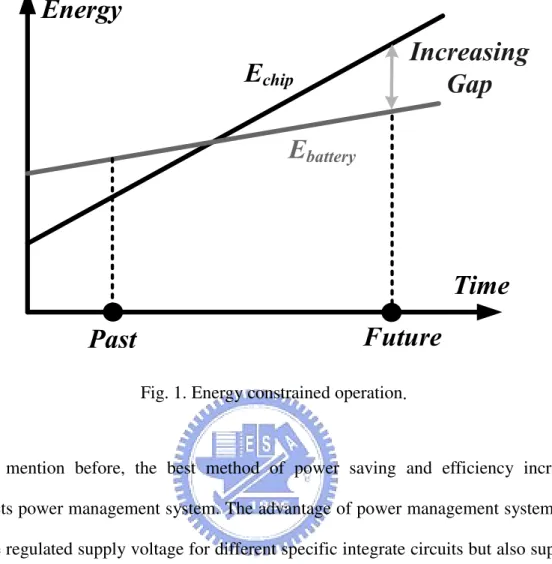
With recent advances in integrated mixed-signal circuits and an increasing demand for low-power multifunction system-on-a-chip (SOC) and extended battery runtime, there is a strong need for the development of efficient on-chip power regulation and distribution. As shown in Fig. 1, the growing of battery energy is not enough to supplying power of chips in the future. That is to say, as increasing chip functionality and complexity will overrun available battery energy budget. To solve this problem, the straightforward method is increasing the quantity of power source. Unfortunately, it is not permitted for portable devices because of convenience. In order to decrease the expenses, the power management systems are utilized to provide the specific regulated voltages without consuming unnecessary batteries.
Time
Past
Future
Energy
E
chipE
batteryIncreasing
Gap
Fig. 1. Energy constrained operation.
As mention before, the best method of power saving and efficiency increasing is constructs power management system. The advantage of power management system not only generate regulated supply voltage for different specific integrate circuits but also suppress the noise which is coupling from battery to electronic devices to extend battery’s lifetime. Take cell phone for example, the basic power management system diagram of cell phone is shown in Fig. 2 [1], a mobile phone may need at least five regulated voltages, one buck converter for DSP core CPU, high PSRR LDO regulators for RF power amplifier and low noise amplifier, one boost converter for cooler LCD panel, LDO regulators for analog base-band, audio and interface applications, and one charge pump for white light LED driver. The system of cell phone will operate in different modes, such as sleeping mode, communication mode and so on. The control unit is needed to control the internal power management block enable or disable, respectively. That is to say, by using control unit can enhance system efficiency of power supply circuits, such as linear regulators, switching regulators and charge pumps. The ability
of saving power and efficiency increasing, that is why power management system playing an important roles in the field of electronics, especially for portable devices.
Fig. 2. Power management system diagram of cell phone.[1]
1.2 Classification of Voltage Regulators
In this section, three kinds of voltage regulators will be introduced briefly, including linear regulators, switched capacitor circuits and switching regulators. Finally, a brief comparison will be given about three types of voltage regulators. The comparisons included circuit complexity, cost, efficiency, load ability and so on.
1.2.1 Linear Regulator
The basic structure of linear regulator is shown in Fig. 3[2], it also called low drop-out (LDO) voltage regulator because there is a drop out voltage (Vdropout ) between input and
output pin about 100~500mV. The power MOSFET has equivalent resistor (RDS) from input
to output, so the power MOSFET size should be well designed to fit the regulated output voltage and load ability. The linear regulator main control circuit was error amplifier, it could adopt output voltage information form resistive feedback network (VFB) then compare to
reference voltage (VREF). After error amplifier operation, it could immediately adjust input
and output difference then control the gate of power MOSFET to supply load current.
The features of linear regulator are described as follows. Firstly, the linear regulator whole circuit is simple and compact, so the die size is smaller than other voltage regulators. And secondly, linear regulator is easy to use, instead of using inductor to transfer energy, the linear regulator just adding two capacitors at input and output pin respectively. As a result, it not only can reduces Printed-circuit board (PCB) area but also cost down. Thirdly, linear regulator only uses resistive feedback network and error amplifier output analogy signal to control power MOSFET, it doesn’t use any switching base circuits. So this kind of regulator has no Electro Magnetic Interference (EMI) and no output ripple, there are very suit for audio, analog and RF circuit applications. Finally, because of without dual storage components, the linear regulator only can do buck regulation. The efficiency is proportional to output voltage and the highest efficiency occurs that output voltage is near to input voltage.
1.2.2 Charge Pump
The basic structure of two-phase charge pump regulator is shown in Fig. 4[3] [4]. Power stage consists of capacitors (C1 C2) and switches (S1 S2 S3 S4). Detailed operation is described
as follows, during the first phase, switches S1 and S2 turn on and switches S3 and S4. The input
voltage charges capacitor C1 to the input voltage level (VIN). Than during the second phase,
switches S3 and S4 turn on and switches S1 and S2. Because the capacitor C1 still maintained
the charge from the previous phase, the output voltage equals to input voltage adding voltage across the capacitor C1, ideally obtains twice input voltage. Adding hysteric feedback control,
the output can be regulated at desired voltage level.
The features of charge pump are described as follows. Firstly, the charge pump can be operated in both buck and boost types, it depended on the hysteric feedback control and
Load
Oscillator
R
1R
2V
REFC
2C
1S
1S
2S
3S
4V
INV
OUTControl signal
Power stage
reference voltage, but it’s more efficiently at boost type. Secondly, the circuit complexity of charge pump is between linear regulator and switching regulator, which is more compact than switching regulator but more complicated than switching regulator. Thirdly, due to digital rail-to-rail switching clock control, the charge pump suffers from EMI and output noise problems. But this problem doesn’t heavier than switching regulator because of lower operation frequency. Finally, the load ability of charge pump is weak because the ability depends on the output capacitor C2 and switching frequency. That is to say, the larger output
capacitor causes the powerful load ability. Because of light load ability typically, the charge pump is very suit for displaying applications, such as driving the gate of MOSFET to on or off.
1.2.3 Switching Regulator
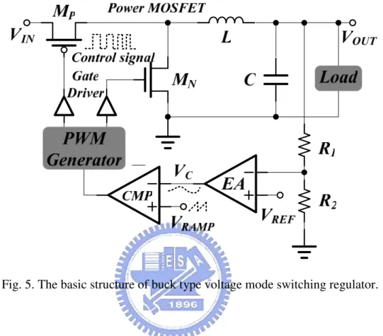
The basic structure of buck type voltage mode switching regulator is shown in Fig. 5[5]. The power stage of switching regulator consists of a couple of complementary power MOSFET (MP MN), passive storage elements inductor (L) and capacitor (C) and resistive
feedback network (R1 R2). Detailed operation is described as follows; the resistors R1 and R2
sensing the variation of output voltage and error amplifier receives the voltage variation information then brings the error signal (VC). The comparator’s inputs receive the error signal
from error amplifier and the ramp signal (VRAMP) from ramp generator, then compares the
quantity between the error signal and the ramp signal to decide the duty cycle. After generating the control signal, the PWM generator control the detail timing to avoid short through current. At last, the purposes of gate drivers are driving huge complementary power MOSFET. At the first subinterval, upper power MOSFET (MP) turns on and lower power
MOSFET (MN) turns off then input voltage source charge the inductor and the capacitor. At
turns off then the inductor will discharge to the capacitor and load. By the above-mentioned, the switching regulator adjusts the output voltage error and regulates to correct voltage.
Fig. 5. The basic structure of buck type voltage mode switching regulator.
The features of switching regulator are described as follows. Firstly, due to the storage components such as inductor and capacitor, the switching regulator can operate in three kinds of type including buck, boost and buck-boost mode. But the more external components cause the bigger PCB size and cost. Secondly, because of switching based circuits, it suffers from EMI and noise problems critically, it will take circuit layout into consideration to avoid EMI and noise problems. Finally, the load ability of switching regulator is the largest which is in the range about hundreds of milliamps to several amps, so the efficiency of switching regulator is the highest at heavy loading, up to 90%. But operating at light loading will decline.
1.2.4 Comparison
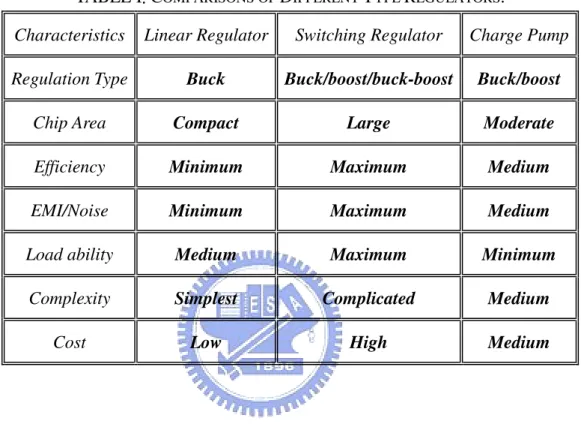
disadvantages. How to choose the best voltage regulator as power supply depend on the electronic applications characteristics and specifications. The comparison of different type voltage regulator is listed in TABLE I.
1.3 Motivation
Conventionally, the switching frequency of current mode DC-DC buck converter operated in the range of hundreds of Kilo-Hertz to several Mega-Hertz. The larger output filter such as inductor and capacitor are placed to off-chip inevitably. To reduce the size of output filter, the straightforward way is increasing the switching frequency. Owing to higher switching frequency, the on-chip output filter in DC-DC switching converter is possible in the future. Meanwhile, with the development of SOC system, a compact solution is needed to reduce the footprint area effectively of the power management module. Besides, the operating voltage of the SOC system is too low to have better signal-to-noise ratio, the high performance voltage regulator needed to generate a regulated and steady supply voltage. In
TABLE I. COMPARISONS OF DIFFERENT TYPE REGULATORS.
Characteristics Linear Regulator Switching Regulator Charge Pump
Regulation Type Buck Buck/boost/buck-boost Buck/boost
Chip Area Compact Large Moderate
Efficiency Minimum Maximum Medium
EMI/Noise Minimum Maximum Medium
Load ability Medium Maximum Minimum
Complexity Simplest Complicated Medium
this part, the current mode technique is used to obtain better line and load regulations. So the implementation of switching frequency 20MHZ current domain DC-DC buck converter is presented base on the above-mentioned motivations.
Although, the higher switching frequency will seriously affect not only current sensing accuracy and response time but also other kind of system circuits. The 20MHz system circuit design is also shown in this thesis.
1.4 Thesis Organization
The thesis introduces the basic knowledge of current mode switching regulator in the Chapter 2. In the Chapter 3, the design and architecture of high switching dc-dc buck converter in current domain control are presented. Base on 20MHz current domain PWM control system, the internal overall circuit implementation and simulation results are shown in Chapter 4. Finally, the whole system chip simulation, system specification, conclusions and future work are presented in Chapter 5.
Chapter 2
Basic Knowledge of Switching
Regulator
In the chapter 2, the basic knowledge of switching regulator is presented. In section 2.1, the three kinds of DC-DC converter topologies are introduced including conversion ratio and power stage structure. The next section 2.2 will show three kinds of controlling modulator including pulse width modulation (PWM), pulse frequency modulation (PFM) and hysteretic control technique. The control principle of current mode buck converter including CCM (continuous conduction mode) and DCM (discontinuous conduction mode) operation and small signal analysis respectively are shown in the section 2.3. At last, the Characteristics and performance specification of buck converter are presented in the section 2.4.
2.1 Topologies of DC-DC Converter
This section introduces three converter topologies of switching regulator, according to the placement of components can combine to buck, boost, and buck–boost types, as shown in Fig. 6[5] [6] [7]. The converter consists of storage element; power MOSFET as the switch to drive large current by control signal and diode as another current passage to charge or discharge output load. The control signal translated the energy from input to output by passing the power MOSFET and regulates output to desire voltage.
The buck converter only can translate high input voltage to low output voltage. Contrarily, the boost converter only can translate low input voltage to high output voltage. The buck-boost can regulate desired output voltage even the input voltage operating at higher or lower than the output. A briefly comparison of the three converter topologies characteristic are listed in the TABLE II. The conversion ratio is defined as the power MOSFET on time
during one switching cycle.
(a) Buck type DC-DC converter
(a) Boost type DC-DC converter
(a) Buck-Boost type DC-DC converter Fig. 6. Three basic topologies of DC-DC converter.
2.2 Technologies of Controlling Modulator
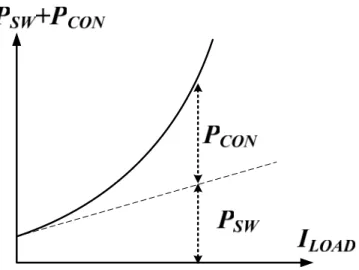
Although the switching converter have high conversion efficiency, but at different load conditions the power will be wasted and result in efficiency reduction. The power consumption can be divided into three parts. The first part is the large current pass to power MOSFET, due to the pass of power MOSFET can be equaled to a resistor (RON), it will result
to a power losses. This power consumption is also called conduction loss (PCON) and express
as follows:
2
CON OUT ON
P
=
I
R
(1)The second part is switching on and off alternately of the power MOSFET, as a results, the gate parasitic large capacitor of power MOSFET alternately charging and discharging. There is a big loss of the converter and this power consumption is also called switching loss (PSW) and express as follows:
2
(
)
SW GP GN IN SW
P
=
C
+
C
V
F
(2) The CGP and CGN are represented as the gate parasitic capacitors of power PMOSFETand power NMOSFET respectively. VIN is represented the input voltage and FSW is
represented the switching frequency. The final part is idle mode that is the condition of the converter operating in no loading. Although there is no load at output, but the converter still
TABLE II. COMPARISONS OF CONVERTER TOPOLOGIES
Topology Buck converter Boost converter Buck-Boost converter
Conversion Ratio OUT
IN V D V = (CCM) 1 1-OUT IN V V = D(CCM) - 1-OUT IN V D V = D(CCM) Conversion Type Only Step-down Only Step-up
D>0.5 doing Step-up D<0.5 doing Step-down
can regulate the output voltage, this moment the current consumption of internal controller is called quiescent current. And the system power loss (PSYS) is defined the multiplication of
quiescent current and input voltage. The efficiency of DC-DC converter is defined the ratio of the output power and input power including the power loss can be expressed as follows.
100%
out OUT OUT
in OUT LOSS OUT SW CON SYS
P
P
P
Efficiency
P
P
P
P
P
P
P
=
=
=
×
+
+
+
+
(3)As above-mentioned, the main power loss of heavy loading condition is PCON because
the large current will flow into the pass power MOSFET and generates larger power loss. Contrarily, the main power losses of light loading condition are PCON and PSYS, the solution to
reduce power loss at light loading is decreases the frequency of control signal. The best way to increase efficiency is changes the control modulation.
The most three basic controlling technology is PWM (Pulse Width Modulation), PFM (Pulse Frequency Modulation) and hysteretic control technique which is introduced in section 2.2.1, 2.2.2 and 2.2.3 respectively.
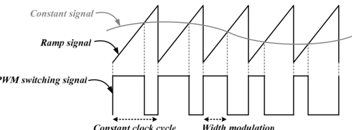
2.2.1 Pulse Width Modulation (PWM)
Operating with PWM control, the power MOSFET are controlled by a constant clock cycle, the PWM control waveform is shown in Fig. 7 [5] [6]. While the ramp signal is lower than the control signal, the PWM signal at high level; the ramp signal is higher than the control signal, the PWM signal changes to low level. The main modulation is change the width of every clock cycle by the control signal and the output voltage is determined by the duty ratio of the PWM signal.
About the power consumption of Pulse Width Modulation focus on the conduction and switching loss, total power loss is expressed as follows.
2 2
(
)
SW CON OUT Duty GP GN IN SW
As shown in Eq. 4, operating at PWM control the switching frequency is constant but output current varies with loading. That is to say, the switching loss is invariable with load but conduction loss will increase with the output loading, as shown in Fig. 8.
Fig. 7. Pulse-width modulation waveform.
Fig. 8. Analysis of conduction loss and switching loss at Pulse-width modulation
2.2.2 Pulse Frequency Modulation (PFM)
Operating with PWM control, the power MOSFET are controlled by a vary frequency, the PFM control waveform is shown in Fig. 9[8] [9]. The on-time of PFM controller is constant width and off-time is variable with loading. By controlling the off-time of every
switching cycle can obtain different switching signal to achieve desirable output voltage. Therefore, the smaller output loading can reduce the switching frequency.
About the power consumption of Pulse Frequency Modulation also focus on the conduction and switching loss, total power loss is expressed as Eq. (4). Operating at PFM control both the switching frequency and output current varies with loading. That is to say, the switching loss and conduction loss will increase with the output loading, as shown in Fig. 10.
Constant pulse width Frequency modulation Light loading
Heavy loading
Fig. 10. Analysis of conduction loss and switching loss at Pulse frequency modulation
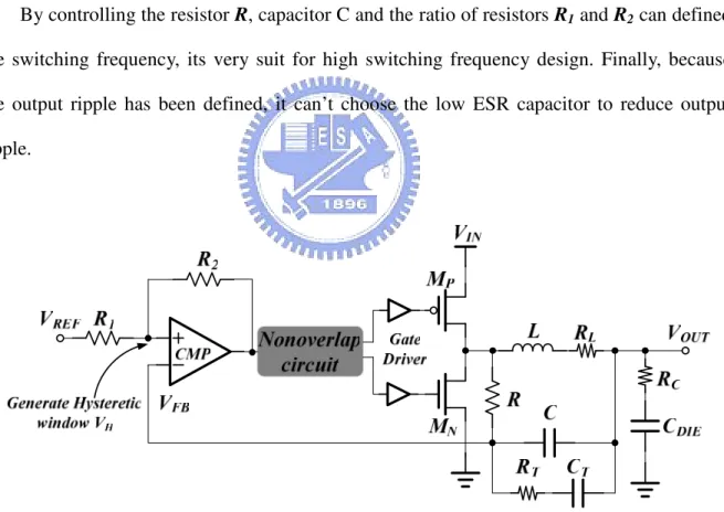
2.2.3 Hysteretic Control technique
The hysteretic controller is shown in Fig. 11[10], the main control method is generating a hysteresis window. By controlling the upper and lower boundary to regulate the output voltage, when the feedback voltage touch to the hysteretic upper boundary, the power NMOSPET will turn on and PMOSPET will turn off to discharge the inductor current and feedback voltage will decrease. At the same time, the hysteretic window will change to the lower boundary. While the feedback voltage touch to the hysteretic lower boundary, the power PMOSPET will turn on and the power NMOSPET will turn off to charge the inductor current and feedback voltage will increase. The hysteretic window which is calculating by superposition theorem can be expressed as follows.
The features of hysteretic controller are described as follows; firstly, the main control circuit is comparator and the error amplifier does not be used, so it is no problem about system compensation. Secondly, without using any clock generator, the switching frequency of hysteretic controller is generated by system itself. The following is the calculation of
2 1 2 1
1 2 1 2 1 2 1 2
(
)
(
)
H uppper lower REF IN REF IN
R
R
R
R
V
V
V
V
V
V
V
R
R
R
R
R
R
R
R
=
−
=
+
−
=
feedback voltage variation, as expressed as follows.
The voltage VFBAVG is the average voltage of feedback, ideally is DVIN, the parameter D
the duty ratio of buck converter. Because the hysteresis window variation (VH) equals to
feedback voltage variation (△△△V△VVVFBFBFBFB). Combining the Eq. (5) and Eq. (6), the switching frequency can as expressed as follows.
By controlling the resistor R, capacitor C and the ratio of resistors R1 and R2 can defined
the switching frequency, its very suit for high switching frequency design. Finally, because the output ripple has been defined, it can’t choose the low ESR capacitor to reduce output ripple.
Fig. 11. The block diagram of Hysteretic control technique
0
0
(1
)
FBAVG FB OFF FBAVG IN
FB OFF
dV
V
V
t
V
DV
D T
I
C
C
V
dt
R
t
RC
RC
−
∆
−
=
⇒
=
⇒ ∆
=
=
(6) 1 0 2 0 1 2 0 1(1
)
1
1
(1
)(1
)
IN H FB INR
DV
D T
R
V
V
V
f
D
D
R
R
RC
T
RC
R
−
= ∆
⇒
=
⇒
=
=
−
+
+
(7)2.3 The Theorem of Current Mode Control
The current mode control DC-DC converter has been used for thirty years and the characteristic is added another current loop of whole system to improve the performances of the converter. In other words, there is why the current mode control DC-DC converter hard to be analyzed because of dual-loop controlled. Therefore, the advantage of current-mode control DC-DC converter is providing better line and load regulation than voltage mode control. The complexity of current mode control DC-DC converter is adding the internal inductor current information as shown in Fig. 12 [5] [6].
Load
V
OUTV
INC
L
D
Compensator
CMP
Oscillation
R
SPWM
Generator
V
REF Inductor sensing current Compensation signalVoltage loop
Current loop
Fig. 12. The conventional current-mode buck converter
As shown in Fig. 12, the current mode control buck converter contains the external output voltage loop and internal current loop. Comparing to the voltage mode control, one of the advantages of current loop is improving the frequency response at AC analysis of the
switching regulator. That is to say, normally the conjugate pole of power stage resulting from the inductor and capacitor will be spilt by adding the current loop and the current mode controller only have one dominate pole at power stage. Not only it can increases the bandwidth of the system but also be compensated easily more than the voltage mode control.
In order to do current mode control, the current sensing and the ramp compensation will be included. The current sensing circuit is sensing the inductor current and size down the current order to compare to the voltage feedback control signal, than deciding the pulse width of every cycle. Because of the current mode control will cause the sub-harmonic oscillation, the ramp compensation is used to prevent this problem.
In this section, the detail current-mode buck converter’s operation will be introduced in the Section 2.3.1. The reason why occur to sub-harmonic oscillation is discussed in the Section 2.3.2. To solve this problem, the Section 2.3.3 will describe the condition of ramp compensation. Finally, the CCM and DCM operation mode and small signal analysis for current mode buck switching regulator is shown in the Section 2.3.4 and the Section 2.3.4 respectively.
2.3.1
Operation Principles of Current Mode Buck
Switching Regulator
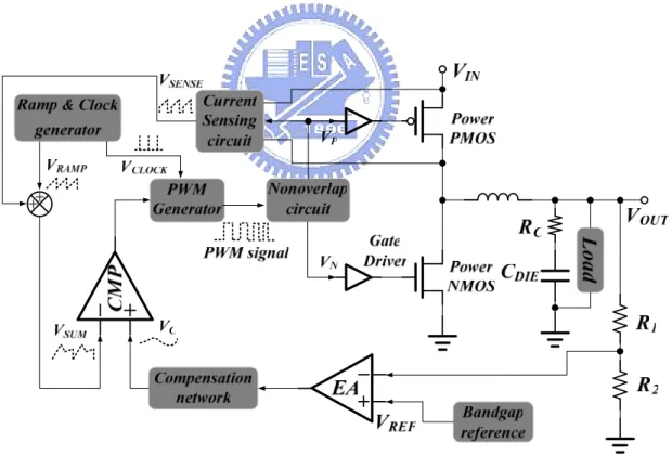
The function blocks of current mode control DC-DC buck converter is shown in Fig. 13[5] [6] [11], the output voltage is dominated by the reference voltage (VREF) which is
generated from bandgap voltage reference. The whole system is controlled by the negative feedback loop, so the close loop gain of whole system must larger to result more precise regulation voltage.
The detail system operation is described as follows, at the beginning of the switching period, the power PMOSFET turned on and the power NMOSFET is turned off, this moment
the current from input source will flow through the power PMOSFET and inductor and will be sensed by the current sensing circuit. The current sense signal (VSENSE) will add to the
compensation ramp signal (VRAMP) and the summation of two signals (VSUM) will compare to
the control signal (VC) from the output of error amplifier. When the summation voltage signal
higher than the control voltage signal, the comparator will change to low level then turn off the power PMOSFET and turn on power NMOSFET. The inductor of output will discharge the current to output capacitor and load. The next period will repeat the steps above mentioned. The operation of current mode controller just like a current source supplies a regulated current to the output. The total gain stage isn’t affects the changing of input voltage, but will affect to voltage mode controller. That is why the line regulation of current mode controls better than voltage mode control.
Fig. 13. The function blocks of the current-mode DC-DC buck converter
By the way, the function of the error amplifier not only increases the close loop gain but also generates the control signal to decide the pulse width signal of power switches. The
compensation network will create a pole-zero pair to do frequency compensation.
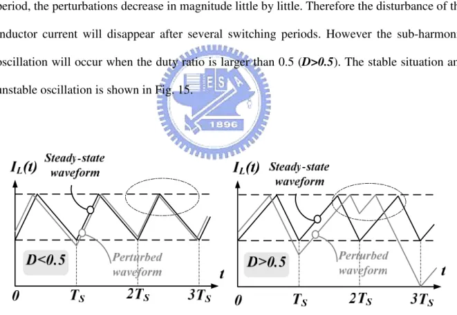
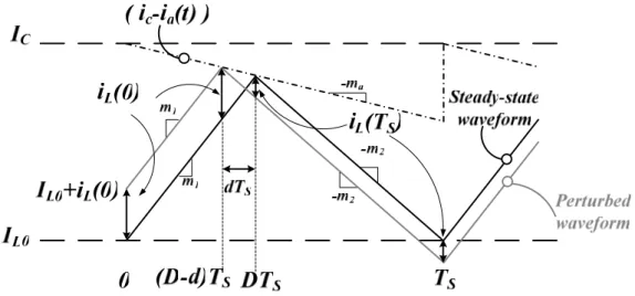
2.3.2 Sub-harmonic Oscillation at Duty Ratio > 0.5
The steady-state waveform and perturbed waveform are analyzed in Fig.14 [5] [12]. The beginning of perturbed error iL(0) can be expressed as the multiplication of the slope m1 and
the interval length –dTs by using the steady-state waveform. As the following express,
In the same way, The end of perturbed error iL(Ts) can be expressed as the multiplication
of the slope -m2 and the interval length –dTs .
Elimination of the intermediate parameter dTS from Eq. (8) and (9) will become
1
(0)
L si
= −
m dT
(8) 2( )
L s si T
=
m dT
(9)I
L0I
L0+i
L(0)
i
L(0)
Perturbed waveform Steady-state waveformI
Ci
L(T
S)
0
DT
S dTS m1 m1T
S -m2 -m2(D-d)T
SFig. 14. Steady-state and perturbed Inductor Current Waveform
2 ' 1
( )
(0)
(0)
L s L Lm
D
i T
i
i
m
D
=
−
=
−
(10)A similar analysis can be performed during the second switching period, the equation is presented as
After nth switching periods, the perturbation becomes
As shown in Eq. (12), when duty cycle smaller than 0.5 (D<0.5) over each switching period, the perturbations decrease in magnitude little by little. Therefore the disturbance of the inductor current will disappear after several switching periods. However the sub-harmonic oscillation will occur when the duty ratio is larger than 0.5 (D>0.5). The stable situation and unstable oscillation is shown in Fig. 15.
2 ' '
(2 )
( )
(0)
L s L s LD
D
i
T
i T
i
D
D
=
−
=
−
(11)(
)
' '(
)
(
1
)
(0)
n L s L s LD
D
i nT
i
n
T
i
D
D
=
−
−
=
−
(12)2.3.3 Ramp Compensation
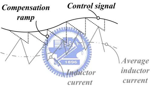
The sub-harmonic oscillation of the current mode controlled converter is an inevasible problem, but as mentioned before, the converter of current mode control can be stable for all duty ratios by adding the compensation ramp to the sensed inductor current signal, as shown in Fig. 16 [5] [6]. The function of the compensated ramp can reduce the gain of the inner current sensing feedback loop in AC analysis to solve the unstable oscillation problem in the current mode controller DC-DC converter.
The compensation theorem is presented in Fig.17, the beginning of perturbed error iL(0)
and the end of perturbed error iL(Ts) are expressed in terms of the m1, m2, ma, and the –dTs. As
the following express,
Average
inductor
current
Inductor
current
Compensation
ramp
Control signal
Fig. 16. Current-mode control signal with the compensation ramp and inductor current
(
1)
(0)
L s ai
= −
dT m
+
m
(13)(
2)
( )
L s s ai T
= −
dT m
−
m
(14)Elimination of the intermediate parameter dTS from Eq. (13) and (14) will become
The same analysis can be used after nth period and leading to
For large n period, the perturbation iL(nTs) will converge to zero provided that the
characteristic value
α
has magnitude less than one. On the contrary, the perturbation iL(nTs)will become large in magnitude when the characteristic value
α
has magnitude greater than one:The common choice of the compensation ramp slop is
This leads to the characteristic value
α
equal to -1 at the maximum duty ratio (D= 1), and the characteristic valueα
in absolute value must be smaller than one (|α| < 1) when operating in the normal duty ratio (0<D<1). That is to say, it will leads to stability for all duty ratio D as the Eq. (18) express,Another common choice of the compensation ramp slop is
The compensation ramp results in the characteristic value
α
to become zero for all duty 2 1( )
(0)
a L s L am
m
i T
i
m
m
−
=
−
+
(15)(
)
2 2 1 1(
)
(
1
)
(0)
(0)
n n a a L s L s L L a am
m
m
m
i nT
i
n
T
i
i
m
m
m
m
α
−
−
=
−
−
=
−
=
+
+
(16) 2 2 1 2 '1
'
(
)
0
1 ;
1
a a a a L sm
m
m
m
D
m
m
m
D
m
D
i nT
when
when
D
α
α
α
−
−
= −
= −
+
+
→
<
→ ∞
−
>
(17) 21
2
am
=
m
(18) 21
2
am
≥
m
(19) 2 am
=
m
(20)circle of the converter. For the reason, iL(Ts) is always to be zero for any iL(0) and the
converter eliminates any one switching period that is called as deadbeat control.
2.3.4 Continuous Conduction Mode (CCM) and Small
Signal Modeling
The characteristic of continuous conduction mode (CCM) discussed in this section including the steady-state signal, the inductor current ripple and the output capacitor voltage then modeling the small signal [5].
When the output average current is larger than the half of inductor peak-to-peak ripple current, the voltage regulator is operated in CCM as shown in Fig. 18 [5]. Because during this mode the inductor current conducts continuously and the minimum current always larger than zero, this situation is usually happening in heavy load condition. For the reason, there are only two subintervals for DC-DC buck converter as shown in Fig. 19(a). Fig. 19(b) and (c) show the first subinterval and second subinterval respectively.
As shown in Fig. 19(b), the inductor voltage, capacitor current and the inductor current slope can be written as Eq. (21), (22) and (23) during the first subinterval. The resistor Rload is
1 -IN OUT V V m L = 2 OUT V m L = −
Fig. 18. The inductor and output current operates in continuous conduction mode.
1
2
V
in(t)
V
out(t)
V
L(t)
L
R
loadC
i
C(t)
(a)
the equivalent loading resistance.
As shown in Fig. 19(c), the inductor voltage, capacitor current and the inductor current slope can be written as Eq. (24), (25) and (26) during the second subinterval.
According to inductor voltage second balance, the voltage conversion ratio D is calculated as Eq. (27). The output voltage increases as conversion ratio D increasing, and ideal case tends to input voltage as D tends to one.
Finally, the inductor current ripple and capacitor voltage ripple can be written as Eq. (28) and Eq. (29) respectively.
( )
( )
( )
L L IN OUTdi
V t
V
t
V
t
L
dt
=
−
=
(21)( )
( )
( )
OUT C L loadV
t
dV
I
t
C
I
t
dt
R
=
=
−
(22) 1( )
( )
( )
IN OUT L LV
t
V
t
di
V t
m
dt
L
L
−
=
=
=
(23)( )
( )
L L OUTdi
V t
V
t
L
dt
= −
=
(24)( )
( )
( )
OUT C L loadV
t
dV
I
t
C
I
t
dt
R
=
=
−
(25) 2( )
( )
OUT L LV
t
di
V t
m
dt
L
L
=
=
= −
(26)(
)
(
) (
1
)
0 ,
out1
IN OUT s OUT s inV
V
V
DT
V
D T
D
V
D
−
⋅
+ −
⋅
−
=
=
=
(27) 1(Changing in )=(Slope
) (The first subinterval time
)
2
2
L S IN OUT IN OUT L S Li
m
DT
V
V
V
V
i
DT
i
DTs
L
L
⋅
−
−
⇒
∆ =
⋅
⇒
∆ =
⋅
(28)(Changing in charge)=(Changing in voltage) (Capacitor )
1
2
2
2
8
L S L OUT OUTC
Ts
i T
Q
i
V
C
V
C
⋅
∆
⇒
= ∆
= ∆
⋅
⇒ ∆
=
(29)The small signal modeling of CCM current mode buck converter only needs to model the average value of a length of switching period. Therefore, the switching ripple of inductor and capacitor must be ignored. For example, the average signal x(t) over an interval of length TS
can be calculated as〈〈〈〈X(t)〉〉〉〉Ts is expressed as follows.
Hence the low frequency underlying ac variations of the inductor and capacitor waveforms can be model by equations of the form:
When the system operates at any transient, the average waveforms can be divided into corresponding quiescent values and the equivalent small ac variations which are shown in Eq. (34).
The Eq. (31) ~ Eq. (33) cab be rewritten as Eq. (35), (36) and (37).
( )
1
S( )
S t T T t SX t
x
d
T
τ τ
+=
∫
(30)( )
'( )
S S S S L T in T out T out TV
=
V
−
V
d t
+ −
V
d t
(31)( )
'( )
S S S S S out T out T C T L T L T load loadV
V
i
i
d t
i
d t
R
R
=
−
+
−
(32)( )
S S in T L Ti
=
i
d t
(33)ˆ ( )
ˆ ( )
ˆ ( )
ˆ ( )
ˆ
( )
( )
S S S S in T in inout T out out
L T L L in T in in
V
V
v t
V
V
v
t
i
I
i t
i
I
i t
d t
D
d t
=
+
=
+
=
+
=
+
=
+
(34)(
)
[
]
(
)
[
]
(
)
ˆ
ˆ
ˆ
ˆ
ˆ
ˆ
'
L Lin in out out out out
d I
i
L
V
v
V
v
D
d
V
v
D
d
dt
+
In order to get the linear system, the nonlinear ac terms must be neglected. That is to say, the second order nonlinear terms in magnitude of the equations above-mentioned are much smaller than the first order terms, so it can be ignored. And linear equation is given by
And the small signal ac equivalent circuit model can be built as Fig. 20.
According to Fig. 20, control-to-output transfer function could be obtained by
(
ˆ
)
ˆ
ˆ
(
ˆ
)
ˆ
ˆ
(
ˆ
)
'
out out out out out out
L L L L load load
d V
v
V
v
V
v
C
I
i
D
d
I
i
D
d
dt
R
R
+
+
+
=
+
−
+
+
+
−
−
(36)(
)
(
ˆ
)
ˆ
ˆ
in in L LI
+
i
=
I
+
i
D
+
d
(37)ˆ
ˆ
ˆ
ˆ
ˆ
ˆ
ˆ
ˆ
ˆ
ˆ
L in in out out C L load in L Lv
dV
Dv
v
v
i
i
R
i
I d
Di
=
+
−
=
−
=
+
(38)ˆ
inv
ˆ
Ld I
⋅
ˆ
ind V
⋅
ˆ
Li
ˆ
outv
Fig. 20. The small signal ac equivalent circuit model of CCM condition.
0 2 ˆ ( ) 0 0 0
ˆ ( )
1
1
( )
,
,
ˆ( )
1
in out out vd load v tv
t
V
C
G
s
Q
R
D
L
LC
d t
S
S
Q
ω
ω
ω
==
=
⋅
=
=
+
+
⋅
(39)Line-to-output transfer function could be obtained by
2.3.5 Discontinuous Conduction Mode (DCM) and Small
Signal Modeling
The characteristic of discontinuous conduction mode (DCM) discussed in this section including the steady-state signal, the inductor current ripple and the output capacitor voltage then modeling the small signal [5]. When the output average current is smaller than the half of inductor peak-to-peak ripple current, the voltage regulator is operated in DCM as shown in Fig. 21[5]. Because during this mode the inductor current conducts discontinuously and the minimum current is equal to zero, this situation is usually happening in light load condition. For the reason, there are three subintervals for DC-DC buck converter, the first and the second subinterval structures are the same as in Fig. 19(b) and the Fig. 19(c) respectively. The additional third subinterval for DC-DC converter is shown in Fig. 22.
0 2 ˆ ( ) 0 0 0
ˆ ( )
1
1
( )
,
,
ˆ ( )
1
out vg load in d tv
t
C
G
s
D
Q
R
v t
S
S
L
LC
Q
ω
ω
ω
==
=
⋅
=
=
+
+
⋅
(40) 1 in out PK SV
V
i
D T
L
−
=
As shown in Fig. 21, the DCM operation can divided into three subintervals, the three symbols D1, D2, and D3 is defined during one switching cycle. The inductor voltage, capacitor
current and the inductor current slope equations of the first and the two subintervals are shown in Eq. (21) ~ (26). The third subinterval is happening while the power PMOSFET and he power NMOSFET are both turn off, the energy stored in output capacitor discharges to output load and the descriptions are written in Eq. (41)
According to inductor voltage second balance, the voltage conversion ratio D is calculated as Eq. (42).
D1 is conversion ratio and D2 need to obtain by inductor current as calculate in Eq. (43)
and Eq. (44).
Fig. 22. The third subinterval of discontinuous conduction mode.
3
0,
out,
0
L C loadV
V
i
m
R
=
= −
=
(41)(
)
(
)
1 1 2 3 1 20
0 ,
out in out s out s S inV
D
V
V
D T
V
D T
D T
D
V
D
D
−
⋅
+
−
⋅
+
⋅
=
=
=
+
(42) 1 1(
)
in out L S PK SV
V
i D T
i
D T
L
−
=
=
(43)Combination the Eq. (43) and Eq. (44) can obtain Eq. (45).
And the Eq. (42) can be translated as follows.
Combination the Eq. (45) and Eq. (46) can obtain Eq. (47).
After calculation the relation between input voltage and output voltage can be expressed as follows.
As shown in Eq. (48), when the DC-DC converter operated in discontinuous Conduction Mode, input voltage and output voltage are not only relating to duty ratio but also in relationship with inductor value, switching frequency and output equivalent loading resistance.
The small signal model of DCM operation for buck converter can use the similar method as CCM operation. Symbols v1, v2, i1 and i2 are assumed to be the terminal voltages and
currents of switching network as illustrated in Fig. 23.
1 2 0