基於一百奈米製程之具區塊層級最佳化的複合式溫度感應功率管理系統
78
0
0
全文
(2) 基於一百奈米製程之具區塊層級最佳化的複合式溫度感應 功率管理系統 A Comprehensive Thermal-Aware Power Management System with Block-Level Optimization in 100nm CMOS Technology 研 究 生:詹偉閔 指導教授:闕河鳴. Student: Wei-Min Chan Advisor: Dr. Herming Chiueh. 博士. 國 立 交 通 大 學 電 信 工 程 學 系 碩 士 班 碩 士 論 文. A Thesis Submitted to Institute of Communication Engineering College of Electrical Engineering and Computer Science National Chiao Tung University in Partial Fulfillment of the Requirements for the Degree of Master of Science in Communication Engineering September 2005 Hsinchu, Taiwan. 中 華 民 國 九 十 四 年 九 月.
(3) Abstract. 基於一百奈米製程之具區塊層級最佳化的複合式溫度感應 功率管理系統 研究生:詹偉閔. 指導教授:闕河鳴. 博士. 國立交通大學 電信工程學系碩士班. 摘要. 由於電池壽命有限的緣故,現今的單晶片整合與手攜式系統強調低功率技術 的應用。傳統的功率管理設計主要是針對動態功率損耗的降低,而最近的設計則 開始將靜態功率損耗納入考量,因為在奈米製程下漏電流逐漸成為不可忽略的要 素。最新的研究善用了單晶片設計思維的模組化特性,發展出區塊層級的控制技 術來降低功率損耗,然而區塊之間的溫差對於單晶片系統設計所帶來的影響卻鮮 少被討論。職是之故,本論文提出了複合式熱感應功率管理及其區塊層級的最佳 化。所提出的設計應用了多種低功率技術來控制晶片內不同的功率損耗來源,同 時顧及溫差所帶來的影響以維持各區塊間效能的一致性。模擬結果顯示,本設計 對於電路的穩定性有顯著的提升,而對於漏電流也得到有效的鉗制。此模擬結果 基於台積電一百奈米互補式金氧半導體製程。. A Comprehensive Thermal-Aware Power Management System with Block-Level Optimization in 100nm CMOS Technology. I.
(4) Abstract. A Comprehensive Thermal-Aware Power Management System with Block-Level Optimization in 100nm CMOS Technology Student: Wei-Min Chan. Advisor: Dr. Herming Chiueh. SoC Design Lab, Department of Communication Engineering, College of Electrical and Computer Engineering, National Chiao Tung University Hsin-Chu 30050, Taiwan. Abstract Modern SoC integrations and mobile systems have emphasized low power techniques due to shortage of battery life. Conventional power management designs focused on the reduction of dynamic power consumption, recent designs begin to take leakage power into consideration since it becomes an important factor in nano-scale CMOS technology. Latest development has taken advantage of modularity in SoC design methodology to develop the block-level control technique for power reductions. However, thermal gradient over the system and its impacts to SoC designs are barely discussed. In this thesis, a block-level optimization of comprehensive thermal aware power management is presented. The proposed design applies several low power techniques to control different power sources and handles thermal impacts to provide performance coherence. As a result, optimal power reductions and performance coherence can be guaranteed within the whole system. The simulation results show a significant improvement in stability and leakage power reduction for most circuitries. These results are based on TSMC 100nm CMOS technology.. A Comprehensive Thermal-Aware Power Management System with Block-Level Optimization in 100nm CMOS Technology. II.
(5) Acknowledgement. Acknowledgement 本篇碩士論文得以順利完成,首先要感謝的是我的指導教授闕河鳴博士。闕 老師總在研究遇到瓶頸的時候給予寶貴的建議,使我得以突破與進步。除此之 外,老師在平日培養學生獨立思考與分析問題的能力,更使我在研究領域建立正 確的態度。. 其次,感謝漳源、庭瑋、明崇、芳如,四位同窗在我研究上與生活上,給予 諸多的幫助與指教,尤其懷念為了完成實驗而一同挑燈夜戰的時光。在此也謝謝 學弟們的支持與幫忙,有了各位晶片系統設計實驗室成員的陪伴,才讓我有這麼 一段快樂且充實的研究經驗。另外再感謝的是交大電子所博士班的華重憲學長, 給予許多理論和實驗的寶貴建議。. 最後,我要感謝父母的栽培,以及所有關心我的家人與朋友,唯有藉著大家 的愛護和幫忙,才能造就今日的我。. 我誠心感謝上述提攜或幫助過我的你們,謝謝大家並祝福大家。. 詹偉閔 中華民國九十四年九月於新竹. A Comprehensive Thermal-Aware Power Management System with Block-Level Optimization in 100nm CMOS Technology. III.
(6) Content. Content 中文摘要 English Abstract Acknowledgment Content List of Tables List of Figures. Ⅰ Ⅱ Ⅲ Ⅳ Ⅵ Ⅶ. Chapter 1 Introduction. 1. 1.1 Motivation 1.2 Organization. 1 6. Chapter 2 Overview of Low Power Techniques 2.1 Power Source Categories 2.1.1 Dynamic Power 2.1.2 Short-Circuit Power 2.1.3 Leakage Power 2.1.4 Summary 2.2 Low Power Techniques 2.2.1 Dynamic Voltage Scaling 2.2.2 Clock Gating 2.2.3 Power Gating 2.2.4 Body Bias 2.2.5 Voltage Islands 2.2.6 Summary 2.3 Enhanced Intel SpeedStep® Technology 2.4 Summary. Chapter 3 Comprehensive Thermal-Aware Power Management 3.1 System Design of CTAPM 3.1.1 Architecture Map 3.1.2 Control State Machine 3.1.3 Look-Up Table Design 3.2 Test Vehicle. 7 7 7 8 8 11 12 12 14 16 18 19 21 22 27. 28 28 29 31 32 34. A Comprehensive Thermal-Aware Power Management System with Block-Level Optimization in 100nm CMOS Technology. IV.
(7) Content. 3.3 Analysis Flow. 36. Chapter 4 Power Analysis. 38. 4.1 Power Gating Analysis 4.1.1 Device Leakage Characteristics 4.1.2 Sleep Transistor Type Selection 4.1.3 Sleep Transistor Sizing 4.1.4 Summary 4.2 DVS Analysis 4.2.1 Characteristics Simulation 4.2.2 VDD Look-Up Table Construction 4.3 RBB Analysis 4.4 FBB Analysis 4.5 Discussion 4.6 Summary. 38 38 39 41 43 44 44 48 50 53 60 62. Chapter 5 Conclusion. 63. 5.1 Conclusion 5.2 Future Works. 63 64. Bibliography. 65. A Comprehensive Thermal-Aware Power Management System with Block-Level Optimization in 100nm CMOS Technology. V.
(8) List of Tables. List of Tables Table 2.1 Table 2.2 Table 2.3 Table 3.1 Table 4.1 Table 4.2 Table 4.3 Table 4.4. Summary of circuit-level low power techniques Voltage specifications of Intel Pentium® M Processor State and control signal definitions of Intel Pentium® M processor State definitions and functionalities of CTAPM Comparison of different sleep transistor types Numerical VDD look-up table for CTAPM Logical VDD look-up table for CTAPM Comparison of different sleep transistor types concerning about power gating and reverse body bias. 21 24 25 32 41 49 49 60. A Comprehensive Thermal-Aware Power Management System with Block-Level Optimization in 100nm CMOS Technology. VI.
(9) List of Figures. List of Figures Figure 1.1 Figure 1.2 Figure 1.3 Figure 2.1 Figure 2.2 Figure 2.3 Figure 2.4 Figure 2.5 Figure 2.6 Figure 2.7 Figure 2.8 Figure 2.9 Figure 2.10 Figure 2.11 Figure 2.12 Figure 2.13 Figure 2.14 Figure 2.15 Figure 2.16 Figure 3.1 Figure 3.2 Figure 3.3 Figure 3.4 Figure 3.5 Figure 3.6 Figure 3.7 Figure 3.8 Figure 3.9 Figure 4.1. Thermal impact to operating frequency of a ring oscillator in TSMC 100nm CMOS technology Thermal impact to power consumption of a ring oscillator in TSMC 100nm CMOS technology Thermal impact to leakage power of a ring oscillator in TSMC 100nm CMOS technology Cause of short-circuit power Summary of leakage current mechanisms of deep-submicrometer transistors Components of gate-tunneling leakage current Processor usage model Conventional hardware-feedback DVS system architecture Improved software-feedback DVS system architecture Illustration of clock gating Operating timing diagram of clock gating Illustration of power gating Different sleep transistor types for power gating Block diagram of two enhanced cut-off schemes Schematic diagram of Vth-hopping. 3 4 5 8 9. 11 12 13 14 15 15 16 17 17 18 Design example utilizing both body bias and power gating 19 Design styles with dual supply voltages 20 Dynamic voltage scaling cycle 23 Low power state machine of Intel Pentium® M Processor 24 Illustration for the functionality of CTAPM 29 Architecture of proposed comprehensive thermal-aware power 30 management unit Low power state machine for CTAPM 31 Diagram of the look-up table design for CTAPM 33 Illustration of the FBB look-up tables 33 A 101-stage ring oscillator used as the test vehicle 34 Layout illustration of the 101-stage ring oscillator 35 Triple-well technology 35 Analysis flow for experiments 36 Device leakage simulation of TSMC 100nm CMOS technology 39. A Comprehensive Thermal-Aware Power Management System with Block-Level Optimization in 100nm CMOS Technology. VII.
(10) List of Figures. Figure 4.2 Figure 4.3. Figure 4.4. Figure 4.5 Figure 4.6 Figure 4.7 Figure 4.8 Figure 4.9 Figure 4.10 Figure 4.11 Figure 4.12 Figure 4.13 Figure 4.14 Figure 4.15 Figure 4.16 Figure 4.17 Figure 4.18 Figure 4.19. Speed comparison of different kinds of the sleep transistor of the ring oscillator under TSMC 100nm CMOS technology Relationship between frequency/power/virtual ground and NMOS sleep transistor width of the ring oscillator under TSMC 100nm CMOS technology Relationship between leakage power and NMOS sleep transistor width of the ring oscillator under TSMC 100nm CMOS technology Relationships between operating frequency and supply voltage in five different technology corners Relationships between power consumption and supply voltage in five different technology corners Relationships between operating frequency and supply voltage in eight different temperature levels Relationships between power consumption and supply voltage in eight different temperature levels Relationships between leakage power and reverse body bias in different applying methods Relationships between leakage power and reverse body bias co-working with power gating in different applying methods Optimum RBB voltage for 130nm technology Relationship between operating frequency and temperature in five technology corners for the high VDD zone. 40 42. 43. 45 46 47 48 51 52 53 54. Relationship between operating frequency and temperature in 55 five technology corners for the low VDD zone Relationship between operating frequency and forward body 56 bias at 25°C in the high VDD zone Relationship between operating frequency and forward body 57 bias at 125°C in the high VDD zone Relationship between operating frequency and forward body bias at 25°C in the middle VDD zone Illustration of FBB application efficiency Comparison of power consumptions at 500MHz between different VDD and FBB voltages Simplified version of the CTAPM unit architecture. 58 59 59 61. A Comprehensive Thermal-Aware Power Management System with Block-Level Optimization in 100nm CMOS Technology. VIII.
(11) Chapter 1 Introduction. Chapter 1 Introduction. 1.1 Motivation Power dissipation in modern VLSI designs has become the most critical issue in System-on-Chip era. The ever increasing on-chip integrations in recent decade have enabled a dramatically increase in system performance and scale. Unfortunately, accompanied with the performance improvement, a significant increase in power dissipation and heat density is introduced [1]. However, in modern VLSI circuitry of mobile systems, especially for handheld audio and video applications, low power considerations are becoming an important issue as battery life and geometry of mobile systems are limited [2, 3]. The demand for increased battery life will require designers to seek out new technologies and circuit techniques to maintain high performance and long operational lifetimes. Therefore, power and thermal issues have become the major limitation of such systems. Low power circuitry designs and architecture-level power reduction techniques have become more important in modern System-on-Chip implementation. Generally, power consumption is categorized to three portions in VLSI circuitry: short circuit, leakage, and dynamic switching power. Traditionally, dynamic switching power is the dominant component of power consumption. However, as scaling trends continue in future generations, leakage power has become comparable to dynamic power, and potentially a dominant component of overall power consumptions [4-6]. Actually, leakage power is approaching 40% of the total power consumption in today’s high-performance microprocessor design [6]. Therefore, unlike previous power reduction methods, modern power management techniques for SoC designs have to deal with static leakage power as equally important as dynamic switching power. Several power reduction techniques can be adopted for modern power management designs, such as dynamic voltage scaling (DVS) [2, 7-11], clock gating [12, 13], power gating [1, 5, 6, 14-17], body bias [6, 18-23], and voltage islands [24-26]. DVS and clock gating can effectively reduce dynamic power consumption, A Comprehensive Thermal-Aware Power Management System with Block-Level Optimization in 100nm CMOS Technology. 1.
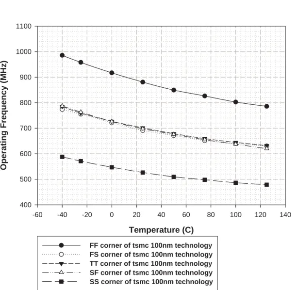
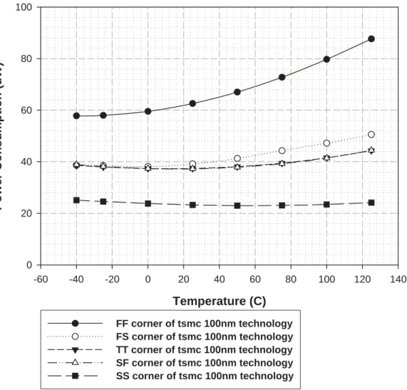
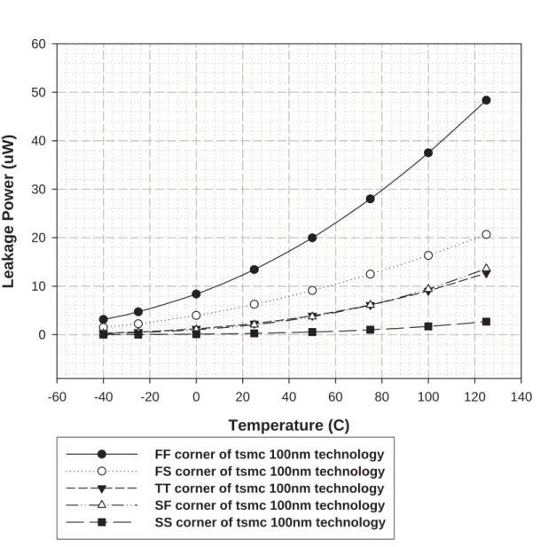
(12) Chapter 1 Introduction. while power gating reduces static leakage power. Forward body bias can increase speed, while reverse body bias reduces power as well. Voltage islands can provide block-level control of power management, which makes control mechanism more flexible. These power reduction techniques are mainly circuit-level to architecture-level, meaning that given corresponding standard cell library, hardware-language coding remains unchanged and current EDA flows are compatible. It is possible to adopt these techniques to already established Software Intellectual Property (Soft-IP), which is in accordance with the concept of IP reuse in SoC designs. Besides battery life, thermal impact is another major reason to utilize power management [8]. Power consumption of the chip contributes thermal impact, such as frequency sacrifice, leakage increase, and even circuit breakdown. Because of high costs of packaging and cooling requirements for reliability, power reduction is also addressed to face thermal impact. However, system temperature is not temporally and spatially constant, so adaptive power control doesn’t imply adaptive thermal control. Thermal gradient over the system and its impact to SoC designs are barely discussed in current power management schemes. Shown in Figure 1.1 to Figure 1.3 is the thermal impact to operating frequency, power consumption, and leakage power of a ring oscillator. We notice that there are about 13% frequency decrease, 18% total power consumption increase in the active mode, and 9X leakage power increase in the standby mode from 0 to 125°C. Functional blocks will not keep performance coherence at the same target frequency due to temperature difference. Leakage problems will become worse and worse as temperature rises. System will become asynchronous and power will not be controlled within specifications if we ignore these changes. Therefore, power management of SoC chip should take temperature variation into consideration. In this thesis, we present a comprehensive thermal-aware power management (CTAPM) architecture and emphasis thermal optimization in block-level control. The proposed design not only deals with dynamic switching power and static leakage power, but also with temperature variation to dynamically adjust performance and power consumption of each block. Our goal is to make power and performance scalable as well as performance coherence between functional blocks in the meantime.. A Comprehensive Thermal-Aware Power Management System with Block-Level Optimization in 100nm CMOS Technology. 2.
(13) Chapter 1 Introduction. 1100. Operating Frequency (MHz). 1000. 900. 800. 700. 600. 500. 400 -60. -40. -20. 0. 20. 40. 60. 80. 100. 120. 140. Temperature (C) FF corner of tsmc 100nm technology FS corner of tsmc 100nm technology TT corner of tsmc 100nm technology SF corner of tsmc 100nm technology SS corner of tsmc 100nm technology. Figure 1.1 Thermal impact to operating frequency of a ring oscillator in TSMC 100nm CMOS technology. Supply voltage is 1.0V.. A Comprehensive Thermal-Aware Power Management System with Block-Level Optimization in 100nm CMOS Technology. 3.
(14) Chapter 1 Introduction. Power Consumption (uW). 100. 80. 60. 40. 20. 0 -60. -40. -20. 0. 20. 40. 60. 80. 100. 120. 140. Temperature (C) FF corner of tsmc 100nm technology FS corner of tsmc 100nm technology TT corner of tsmc 100nm technology SF corner of tsmc 100nm technology SS corner of tsmc 100nm technology. Figure 1.2 Thermal impact to power consumption of a ring oscillator in TSMC 100nm CMOS technology. Supply voltage is 1.0V.. A Comprehensive Thermal-Aware Power Management System with Block-Level Optimization in 100nm CMOS Technology. 4.
(15) Chapter 1 Introduction. 60. Leakage Power (uW). 50. 40. 30. 20. 10. 0. -60. -40. -20. 0. 20. 40. 60. 80. 100. 120. 140. Temperature (C) FF corner of tsmc 100nm technology FS corner of tsmc 100nm technology TT corner of tsmc 100nm technology SF corner of tsmc 100nm technology SS corner of tsmc 100nm technology. Figure 1.3 Thermal impact to leakage power of a ring oscillator in TSMC 100nm CMOS technology. Supply voltage is 1.0V.. A Comprehensive Thermal-Aware Power Management System with Block-Level Optimization in 100nm CMOS Technology. 5.
(16) Chapter 1 Introduction. 1.2 Organization In the beginning of Chapter 2, categories of power sources in digital ICs are discussed. Next comes the overview of low power techniques. After them, the Enhanced Intel SpeedStep® Technology, a state-of-the-art example of power management design, is presented. Finally, contributions and features of our comprehensive thermal-aware power management design end this chapter. In Chapter 3, we propose the CTAPM unit architecture. Possible control flow chart, control state definition, and look-up table design are also introduced in this chapter. This CTAPM is designed to provide dynamic block-level power control and ensure performance coherence between functional blocks. Moreover, the test vehicle and analysis flow for power analysis are described in the end of this chapter. In Chapter 4, the effect and efficiency of low power techniques are discussed. The experimental results of these different circuitry techniques are presented to see if they can provide needed functionalities for our CTAPM design. These results are based on TSMC 100nm CMOS technology, In Chapter 5, conclusions and future works are addressed.. A Comprehensive Thermal-Aware Power Management System with Block-Level Optimization in 100nm CMOS Technology. 6.
(17) Chapter 2 Overview of Low Power Techniques. Chapter 2 Overview of Low Power Techniques. This chapter begins with the classification of power sources in VLSI circuitry. Several low power techniques are examined next to realize their functionalities. Afterwards, the Enhanced Intel SpeedStep® Technology is introduced as an example of modern power management design. Finally, contributions and features of our comprehensive thermal-aware power management (CTAPM) design are summarized in the end of this chapter.. 2.1 Power Source Categories In modern digital integrated circuits, power consumption is categorized to three components: dynamic, short circuit, and static leakage power.. 2.1.1 Dynamic Power Conventionally, dynamic power is the dominant component of total power consumption. Charging and discharging load capacitance contribute this power. Dynamic power is given by. Pdynamic = pt × f clk × C switched × VDD. 2. (2.1). where pt is the switching activity, fclk is the operating frequency, Cswitched is the total effective switched capacitance, and VDD is the supply voltage. Obviously, scaling down VDD is the most efficient way to reduce dynamic power, since dynamic power is proportional to the square of VDD. However, VDD cannot be scaled down unlimitedly because the operating frequency also degrades with lower supply voltage.. A Comprehensive Thermal-Aware Power Management System with Block-Level Optimization in 100nm CMOS Technology. 7.
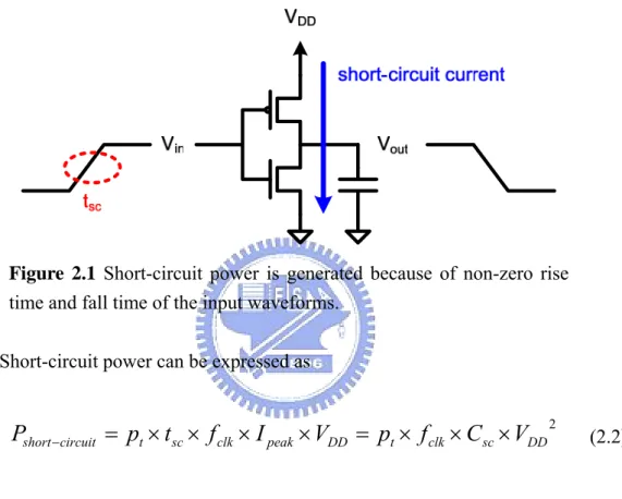
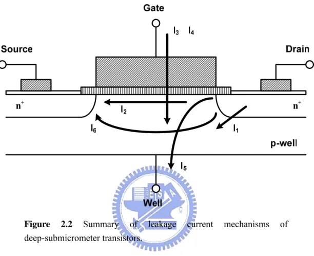
(18) Chapter 2 Overview of Low Power Techniques. 2.1.2 Short-Circuit Power The second component of power consumption is called short-circuit power, which results from non-zero rise time and fall time of the input waveforms. As shown in Figure 2.1, non-zero input rise time and fall time make PMOS and NMOS turn on at the same period of time, setting up a DC path between VDD and ground, therefore introducing the short-circuit current to consume power.. Figure 2.1 Short-circuit power is generated because of non-zero rise time and fall time of the input waveforms. Short-circuit power can be expressed as. Pshort −circuit = pt × t sc × f clk × I peak × VDD = pt × f clk × Csc × VDD. 2. (2.2). where tsc is the time when the DC path exists, Ipeak is the maximum of short-circuit current, and Csc is the equivalent switched capacitance. Just like dynamic power, short-circuit power is also proportional to the switching activity. Besides, if VDD can be scaled down below the sum of absolute values of NMOS and PMOS threshold voltage, which means Vthn + |Vthp|, then short-circuit power will be eliminated because NMOS and PMOS won’t turn on at the same time.. 2.1.3 Leakage Power The third component of power consumption is leakage power, which grows larger and larger in nano-scale CMOS technologies. Leakage current can be divided into several portions, as illustrated in Figure 2.2 [4]. I1 is the reverse-bias pn junction A Comprehensive Thermal-Aware Power Management System with Block-Level Optimization in 100nm CMOS Technology. 8.
(19) Chapter 2 Overview of Low Power Techniques. leakage, I2 is the subthreshold leakage, I3 is the oxide tunneling current, I4 is the gate current due to hot-carrier injection, I5 is the gate-induced drain leakage (GIDL), and I6 is the channel punchthrough current.. Figure 2.2 Summary of leakage deep-submicrometer transistors.. current. mechanisms. of. Among these leakage sources, subthreshold leakage is dominant and can be modeled as [4]. I subth = A × e. (VG − VS −Vth 0 − γ '×VS − η ×V DS ). mVT. × (1 − e. −V DS. VT. ). (2.3). where. A = μ0Cox. − ΔVth W (VT ) 2 × e1.8 × e ηVT Leff. (2.4). A Comprehensive Thermal-Aware Power Management System with Block-Level Optimization in 100nm CMOS Technology. 9.
(20) Chapter 2 Overview of Low Power Techniques. Vth0 is the zero bias threshold voltage, VT is the thermal voltage, γ' is the linearized body effect coefficient, and η is the drain-induced barrier lowing (DIBL) coefficient. μ0 is the zero bias mobility, Cox is the gate oxide capacitance, m is the subthreshold swing coefficient of the transistor, and ∆Vth is a term introduced to account for transistor-to-transistor leakage variations. Equation (2.3) reveals that subthreshold leakage is larger when threshold voltage is lower due to their inverse exponential relationship. It is serious in nanometer devices since threshold voltage follows the scaling trends with the progress of CMOS technology. Subthreshold leakage is the dominant component of leakage power consumption in deep-submicron and nanometer CMOS technologies. However, gate-tunneling leakage has the potential to exceed subthreshold leakage in future generations. The equation of gate tunneling leakage is given by [4]. { − B [1 − (1 − 2. J DT = AEox × e. Vox. φ ox. ) 3 / 2 ]} Eox. (2.5). where. 4 2m* φox q3 A= ,B= 16π 2 hφox 3hq. 3/ 2. (2.6). Vox is the voltage drop across the gate oxide, φ ox is the Si-SiO2 interface barrier height for electrons, and Eox is the field across the oxide. As shown in Figure 2.3 [4], gate-tunneling leakage can be further divided into five components, namely, parasitic leakage current through gate-to-source and gate-to-drain extension overlap region (Igso and Igdo), gate to inverted channel current (Igc) which goes to the source (Igcs) and the drain (Igcd), and the gate to the substrate leakage current (Igb).. A Comprehensive Thermal-Aware Power Management System with Block-Level Optimization in 100nm CMOS Technology. 10.
(21) Chapter 2 Overview of Low Power Techniques. Figure 2.3 Components of gate-tunneling leakage current. Unlike dynamic and short-circuit power which depend on the number of actively switching transistors, leakage power is a function of the total number (or area) of on-chip transistors, independent of their switching activity [1]. Although scaling VDD down also helps to reduce subthreshold and gate-tunneling leakage, its limitations of frequency degrading and noise margin decrease still exist. However, power gating and reverse bias are two effective ways to suppress leakage power, which will be explained later in Section 2.2.. 2.1.4 Summary Power consumption of a VLSI chip can be categorized to three components: dynamic, short circuit, and leakage power. Traditionally, dynamic power is dominant, but leakage power has become comparable to dynamic power in nano-scale CMOS technologies. Subthreshold leakage is the dominant component of leakage power nowadays. However, gate-tunneling leakage has the potential to exceed subthreshold leakage in future generations. Several low power techniques have been proposed to reduce and control power consumption dynamically, such as dynamic voltage scaling (DVS), clock gating, power gating, body bias, and voltage islands. These techniques will be introduced respectively in the next section. A Comprehensive Thermal-Aware Power Management System with Block-Level Optimization in 100nm CMOS Technology. 11.
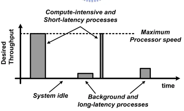
(22) Chapter 2 Overview of Low Power Techniques. 2.2 Low Power Techniques DVS, clock gating, power gating, body bias, and voltage islands are five major circuit-level techniques to reduce power consumption. They deal with different power sources and have individual control mechanisms.. 2.2.1 Dynamic Voltage Scaling Dynamic voltage scaling is the most efficient technique to reduce dynamic power. It also has benefits for leakage power saving. When the required performance of the target system is lower than the maximum performance, supply voltage can be dynamically reduced to the lowest possible extent that ensures proper operation. Significant power reduction is possible, since dynamic power of CMOS circuits is proportional to the square of the supply voltage.. Desired Throughput. Shown in Figure 2.4 is an example of the microprocessor system’s desired throughput as a function of time [9]. The computational requirements can be considered to fall into one of three categories: compute-intensive, low-speed, and idle (standby). Low-speed and long-latency tasks only require a fraction of the full throughput to adequately run. Executing these tasks faster than needed has no discernible benefit. Therefore, the supply voltage has room to be scaled down in this situation to save dynamic power.. Figure 2.4 Processor usage model. A Comprehensive Thermal-Aware Power Management System with Block-Level Optimization in 100nm CMOS Technology. 12.
(23) Chapter 2 Overview of Low Power Techniques. The conventional DVS system architecture is shown in Figure 2.5 [7]. The value of the supply voltage is determined by the computational loading and adjusted by a hard-wired frequency-voltage feedback loop. A ring oscillator, which is the replica of the critical path, is used to model the CMOS circuit delay for given supply voltage. However, this hardware-feedback approach does not provide efficient voltage control and has the following problems [7]: 1. Even in a same chip, critical path may be different along supply voltage, meaning that circuit delay of ring oscillator should have much margin to cover this variation. 2. Since fabrication process technology is different for each chip, circuit delay characteristics may differ a lot, meaning that all chips should be custom-designed to have same frequency-voltage relationship for efficient power reduction. 3. This approach cannot be applied for off-the-shelf processors, since ring oscillator cannot be inserted into ready-made chips. 4. In the multi-processor system, it is desirable to control supply voltages separately for each processor, which is impossible in this approach.. Voltage Regulator fDESIRE +. Σ -. fERR. Switching VVAR Power Supply. fVAR. Desired Frequency Register. Ring Oscillator. Interface with External Systems. I/O Chip. fVAR Memory Chip. Software. Processor Core Processor. Peripheral Chip System Bus. Figure 2.5 Conventional hardware-feedback DVS system architecture. These problems can be solved by the software-feedback approach, as shown in Figure 2.6 [7]. Desired supply voltage is looked up from the device driver. The device driver has two lookup tables: one for frequency-voltage relationship of the chip, and A Comprehensive Thermal-Aware Power Management System with Block-Level Optimization in 100nm CMOS Technology. 13.
(24) Chapter 2 Overview of Low Power Techniques. the other for transition delay to change clock frequency and supply voltage. These lookup tables are programmable and established by physical measuring results. Therefore, this software-feedback approach can prevent the conventional DVS system’s problems.. Figure 2.6 Improved software-feedback DVS system architecture. The concept of software feedback is inspiring and essential in our comprehensive thermal-aware power management design. This concept can be applied to other low power techniques, so that these techniques can be controlled in the same way. Related issues will be discussed in Chapter 3.. 2.2.2 Clock Gating Clock gating is another efficient technique to reduce dynamic power. Clock switching power is a major component of total dynamic power because clock tree represents a very large load and clock signal switches all the time. If we can control and stop clock switching when the system is idle or data remain unchanged, thus unnecessary clock switching power can be saved.. A Comprehensive Thermal-Aware Power Management System with Block-Level Optimization in 100nm CMOS Technology. 14.
(25) Chapter 2 Overview of Low Power Techniques. Shown in Figure 2.7 is an illustration of the clock gating technique. The clk_enable signal is commonly set to high voltage level (logic 1) during normal operation. If the system is idle or data remain unchanged, then clk_enable will be set to low voltage level (logic 0) to stop local gated clock switching. An example of the operating timing diagram is shown in Figure 2.8. Finally, either AND gate or NOR gate can be used to generate gated clock, depending on which trigger type (positive-edge trigger or negative-edge trigger) of sequential elements is selected.. Figure 2.7 Illustration of clock gating.. Global Clock Action. Stall. Stall. Stall. Action. clk_enable. Gated Clock. Figure 2.8 Operating timing diagram of clock gating, which is the positive-edge triggered case.. A Comprehensive Thermal-Aware Power Management System with Block-Level Optimization in 100nm CMOS Technology. 15.
(26) Chapter 2 Overview of Low Power Techniques. 2.2.3 Power Gating Power gating is the most efficient way to reduce leakage power. Figure 2.9 is an illustration of this technique [5]. In the active mode, the ctrl signal remains high, and the power gating devices act as minor power-rail resistance which does not affect the correctness of the function. In the standby mode, however, ctrl is set to low. The power gating devices act as open switches that cut off the direct connection between power supply and internal circuits, so as to reduce leakage current [15].. Figure 2.9 Illustration of power gating. Actually, sleep transistors, as power gating devices, can be PMOS (header-type) or NMOS (footer-type), as shown in Figure 2.10 [15]. Because PMOS sleep transistors require larger silicon area to be capable of sourcing the maximum instantaneous current in the active mode, NMOS is commonly chosen to be power gating devices. Besides, if sleep transistors are turned off more strongly, further leakage reduction can be achieved. Figure 2.11 shows the block diagram of two enhanced cut-off switch schemes having multi-threshold-voltage CMOS (MTCMOS) and variable-threshold-voltage (VTCMOS) [17]. However, using higher threshold voltage transistors as sleep transistors requires extra mask cost for foundry and larger silicon area to be capable of sinking the maximum instantaneous current in the active mode. Therefore, using single threshold voltage transistors as sleep transistors only or utilizing reverse body bias technique to adjust threshold voltage of sleep transistors are more recommendable. A Comprehensive Thermal-Aware Power Management System with Block-Level Optimization in 100nm CMOS Technology. 16.
(27) Chapter 2 Overview of Low Power Techniques. Figure 2.10 (a) NMOS footer-type sleep transistors for power gating. (b) PMOS header-type sleep transistors for power gating.. Figure 2.11 Block diagram of two enhanced cut-off schemes. (a) MTCMOS (b) VTCMOS (also known as reverse body bias).. A Comprehensive Thermal-Aware Power Management System with Block-Level Optimization in 100nm CMOS Technology. 17.
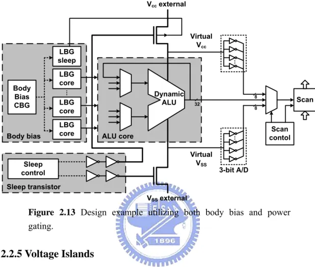
(28) Chapter 2 Overview of Low Power Techniques. 2.2.4 Body Bias Body bias can be applied for either dynamic or leakage power reduction. In the active mode, forward body bias (FBB) is applied to reduce supply voltage to save dynamic power at the same operating frequency. In the standby mode, reverse body bias (RBB) is applied to raise threshold voltage to save leakage power. Figure 2.12 shows the Vth-hopping scheme that the substrate bias of transistors can be dynamically changed [23]. VBSP and VBSN, the body voltage of PMOS and NMOS, are isolated from VDD and ground, connected to two possible voltage levels to adjust the threshold voltage of the target processor. In the active mode, the Vt_low_enable signal is asserted, inducing FBB to lower the threshold voltage, so as to reduce supply voltage to save dynamic power at the same operating frequency. In the standby mode, however, Vt_high_enable is asserted, inducing RBB to raise the threshold voltage of the target processor to save leakage power. The CONT signal represents the operation mode and decides the values of Vt_low_enable and Vt_high_enable. It can also be used to control the discrete frequency levels of the target processor.. Figure 2.12 Schematic diagram of Vth-hopping. As mentioned before, body bias can be combined with power gating technique to provide further leakage power savings. Shown in Figure 2.13 is a design example which applies these two techniques [6]. On the one hand, FBB can compensate part of frequency degradation due to power gating insertion in the active mode. On the other A Comprehensive Thermal-Aware Power Management System with Block-Level Optimization in 100nm CMOS Technology. 18.
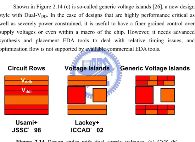
(29) Chapter 2 Overview of Low Power Techniques. hand, RBB can turn off sleep transistors more strongly to further reduce leakage power in the standby mode, which is also known as the VTCMOS cut-off scheme of power gating. Vcc external. Virtual Vcc. LBG sleep. Body Bias CBG. Body bias. LBG core Dynamic ALU. LBG core LBG core. 8 32. Scan. 8. Scan contol. ALU core Virtual VSS. Sleep control. 3-bit A/D. Sleep transistor VSS external. Figure 2.13 Design example utilizing both body bias and power gating.. 2.2.5 Voltage Islands Voltage Islands provide block-level control of the system. In the active mode, local supply voltage can scale down to reduce dynamic power while maintaining the same performance for islands at non-critical paths. In the standby mode, leakage savings are possible when the island is not being used, regardless of whether or not the rest of others are operating. Block-level control makes it easier to spatially optimize the system. The concept of voltage islands was proposed by IBM in 2002 and originated from the use of dual supply voltages (Dual-VDD) [24, 27]. To begin with, gates on critical paths are assigned to operate at higher VDD and non-critical portions of the circuit operate at lower VDD, reducing the total power consumption without degrading performance. For example, clustered voltage scaling (CVS) is a classic design style with Dual-VDD [24], as shown in Figure 2.14(a).. A Comprehensive Thermal-Aware Power Management System with Block-Level Optimization in 100nm CMOS Technology. 19.
(30) Chapter 2 Overview of Low Power Techniques. Afterwards, as shown in Figure 2.14 (b), the concept of voltage islands restores the concept of individual voltage optimization of functional blocks to SoC design [25]. Individual functional blocks of the SoC design can have power characteristics unique from the rest of the design, and can be optimized accordingly. For example, in a system integrating a processor core with on-chip memory and control logic, the processor core may require the highest voltage for performance requirements. However, the on-chip memory and control logic can be operated at low voltage to save dynamic power without compromising system performance. In addition, this macro-based design methodology allows pre-designed standard components to be reused. Shown in Figure 2.14 (c) is so-called generic voltage islands [26], a new design style with Dual-VDD. In the case of designs that are highly performance critical as well as severely power constrained, it is useful to have a finer grained control over supply voltages or even within a macro of the chip. However, it needs advanced synthesis and placement EDA tools to deal with relative timing issues, and optimization flow is not supported by available commercial EDA tools.. Circuit Rows. Voltage Islands. Generic Voltage Islands. Vddh Vddl. Usami+ JSSC 98. Lackey+ ICCAD 02. Figure 2.14 Design styles with dual supply voltages. (a) CVS (b) voltage islands (c) generic voltage islands. Voltage islands itself is a static solution for low power criteria, but it can be combined with power gating to perform dynamic block-level control of leakage power. It can also be combined with DVS to dynamically and spatially reduce active power, since the power supply of each voltage island is separated and isolated.. A Comprehensive Thermal-Aware Power Management System with Block-Level Optimization in 100nm CMOS Technology. 20.
(31) Chapter 2 Overview of Low Power Techniques. 2.2.6 Summary DVS provides overall power reduction by dynamically scaling down the supply voltage. Clock gating saves clock switching power when the system is idle or data remain unchanged by stopping local gated clock switching. These two techniques mainly focus on dynamic power saving. On the contrary, power gating efficiently suppresses leakage power in the standby mode by cutting off the direct connection between power supply and internal circuits. Body bias has two ways to use: FBB and RBB. Forward body bias can reduce dynamic power at the same target frequency or increase speed with the same supply voltage, whereas reverse body bias reduces leakage power by raising threshold voltages of NMOS and PMOS transistors. Moreover, voltage islands provide block-level optimization and spatial flexibility for control mechanism. Table 2.1 is the summary. Table 2.1 Summary of circuit-level low power techniques. Space domain. Dynamic power. Leakage power. saving. saving. Technology. Time domain. Dynamic Voltage Scaling. Yes. Yes. Clock Gating. Yes. Yes. Power Gating. Yes. Forward Body Bias. Yes. Reverse Body Bias. Yes. Yes Yes Yes. Voltage Islands. Yes. Yes. Yes. A Comprehensive Thermal-Aware Power Management System with Block-Level Optimization in 100nm CMOS Technology. 21.
(32) Chapter 2 Overview of Low Power Techniques. 2.3 Enhanced Intel SpeedStep® Technology In this section, the Enhanced Intel SpeedStep® Technology [28], a state-of-the-art example of power management design and widely used in the Intel processor family, is introduced. The old version of this technology enables real-time dynamic switching of the voltage and frequency between two performance modes based on processor demand. However, the Enhanced Intel SpeedStep® Technology enables the processor to switch between multiple frequency and voltage points instead of two. Switching between states is software controlled. Following are the key features of the Enhanced Intel SpeedStep® technology [28]: y Multiple voltage/frequency operating points provide optimal performance at the lowest power. y Voltage/Frequency selection is software controlled by writing to processor model specific registers (MSRs) thus eliminating chipset dependency. – If the target frequency is higher than the current frequency, Vcc is ramped up by placing a new value on the VID pins and the PLL then locks to the new frequency. – If the target frequency is lower than the current frequency, the PLL locks to the new frequency and the Vcc is changed through the VID pin mechanism. – Software transitions are accepted at any time. If a previous transition is in progress, the new transition is deferred until its completion. y Low transition latency and large number of transitions possible per second. – Processor core (including L2 cache) is unavailable for up to 10μs during the frequency transition. y Improved Intel® Thermal Monitor mode. – When the on-die thermal sensor indicates that the die temperature is too high, the processor can automatically perform a transition to a lower frequency/voltage specified in a software programmable MSR. – The processor waits for a fixed time period. If the die temperature is down to acceptable levels, an up transition to the previous frequency/voltage point occurs. – An interrupt is generated for the up and down Intel Thermal Monitor transitions enabling better system level thermal management.. A Comprehensive Thermal-Aware Power Management System with Block-Level Optimization in 100nm CMOS Technology. 22.
(33) Chapter 2 Overview of Low Power Techniques. The Enhanced Intel SpeedStep® Technology used a DVS based mechanism, changing both the voltage as well as the frequency at run time, to adjust the power consumption of the system to the thermal conditions and to maximize the battery life [8]. An example of a DVS cycle is described in Figure 2.15 [8]. Initially, the processor is operating at high VDD and high frequency generating high power. When the on-die thermal sensor indicates that the die temperature is too high, or the workload of the processor is lower than its capability, then the processor halts the execution and locks the phase-locked loop (PLL) at a new frequency. Once finished, the VDD starts changing to a new lower value. The full power saving is achieved once the voltage transition is finished. A frequency transition up is done in reverse order to ensure normal work of the processor. Finally, the target frequency and voltage points are programmable by BIOS or operating system. Table 2.2 is an example of the Enhanced Intel SpeedStep® Technology operating point for Intel Pentium® M Processor [28]. Besides the Enhanced Intel SpeedStep® Technology, the Intel Pentium® M processor supports the AutoHALT Power-Down, Stop Grant, HALT/Grant Snoop, Sleep, DeepSleep, and Deeper Sleep states for optimal power management. Figure 2.16 is its low power state machine and Table 2.3 explains definitions of these states in detail [28].. Figure 2.15 Dynamic voltage scaling cycle.. A Comprehensive Thermal-Aware Power Management System with Block-Level Optimization in 100nm CMOS Technology. 23.
(34) Chapter 2 Overview of Low Power Techniques. Table 2.2 Voltage specifications of Intel Pentium® M Processor. The Intel Pentium® M processor uses six voltage identification pins, VID[5:0], to support automatic selection of power supply voltages. Processor. Frequency (MHz). VDD (V). VID. 2.1. 1.340. 010111. 1.8. 1.276. 011011. 1.6. 1.228. 011110. 1.4. 1.180. 100001. 1.2. 1.132. 100100. 1.0. 1.084. 100111. 0.8. 1.036. 101010. 0.6. 0.988. 101101. 2.1. 1.340. 010111. 1.8. 1.292. 011010. 1.6. 1.244. 011101. 1.4. 1.196. 100000. 1.2. 1.148. 100011. 1.0. 1.100. 100110. 0.8. 1.052. 101001. 0.6. 0.988. 101101. Intel Pentium® M Processor 765. Intel Pentium® M Processor 755. STPCLK# asserted. Normal. STPCLK# deasserted. SLP# asserted. Stop Grant. Sleep SLP# deasserted. STPCLK# asserted. STPCLK# deasserted snoop occurs. AutoHALT snoop serviced. snoop serviced. DPSLP# deasserted. snoop occurs. DPSLP# asserted. core voltage raised. HALT/ Grant Snoop. Deep Sleep. Deep Sleep core voltage lowered. Figure 2.16 Low power state machine of Intel Pentium® M processor.. A Comprehensive Thermal-Aware Power Management System with Block-Level Optimization in 100nm CMOS Technology. 24.
(35) Chapter 2 Overview of Low Power Techniques. Table 2.3 State and control signal definitions of Intel Pentium® M processor. Normal State. This is the normal operating state for the processor.. AutoHALT Power-Down State. AutoHALT Power-Down is a low-power state entered when the processor executes the HALT instruction. While in AutoHALT Power-Down state, the processor will process bus snoops and interrupts.. Stop-Grant State. When the STPCLK# pin is asserted, the Stop-Grant state of the processor is entered 20 bus clocks after the response phase of the processor-issued Stop Grant Acknowledge special bus cycle. While in Stop-Grant state, the processor will process snoops on the FSB and it will latch interrupts delivered on the FSB.. HALT/Grant Snoop State. The processor responds to snoop or interrupt transactions on the FSB while in Stop-Grant state or in AutoHALT Power-Down state. During a snoop or interrupt transaction, the processor enters the HALT/Grant Snoop state.. Sleep State. A low power state in which the processor maintains its context, maintains the PLL, and has stopped all internal clocks. The Sleep state can be entered only from Stop-Grant state. In the Sleep state, the processor is incapable of responding to snoop transactions or latching interrupt signals. No transitions or assertions of signals (with the exception of SLP#, DPSLP# or RESET#) are allowed on the FSB while the processor is in Sleep state.. Deep Sleep State. Deep Sleep state is a very low power state the processor can enter while maintaining context. BCLK may be stopped during the Deep Sleep state for additional platform level power savings. When the processor is in Deep Sleep state, it will not respond to interrupts or snoop transactions.. Deeper Sleep State. This state is functionally identical to the Deep Sleep state but at a lower core voltage.. STPCLK#. STPCLK# (Stop Clock), when asserted, causes the processor to enter a low power Stop-Grant state. The processor issues a Stop-Grant Acknowledge transaction, and stops providing internal clock signals to all processor core units except the FSB and APIC units. The processor continues to snoop bus transactions and service interrupts while in Stop-Grant state. When STPCLK# is deasserted, the processor restarts its internal clock to all units and. A Comprehensive Thermal-Aware Power Management System with Block-Level Optimization in 100nm CMOS Technology. 25.
(36) Chapter 2 Overview of Low Power Techniques. resumes execution. The assertion of STPCLK# has no effect on the bus clock; STPCLK# is an asynchronous input. SLP#. SLP# (Sleep), when asserted in Stop-Grant state, causes the processor to enter the Sleep state. During Sleep state, the processor stops providing internal clock signals to all units, leaving only the Phase-Locked Loop (PLL) still operating. Processors in this state will not recognize snoops or interrupts. The processor will recognize only assertion of the RESET# signal, deassertion of SLP#, and removal of the BCLK input while in Sleep state. If SLP# is deasserted, the processor exits Sleep state and returns to Stop-Grant state, restarting its internal clock signals to the bus and processor core units. If DPSLP# is asserted while in the Sleep state, the processor will exit the Sleep state and transition to the Deep Sleep state.. DPSLP#. DPSLP# when asserted on the platform causes the processor to transition from the Sleep State to the Deep Sleep state. In order to return to the Sleep state, DPSLP# must be deasserted.. In summary, the Intel Pentium® M processor applies DVS in the active mode, which means utilizing the Enhanced Intel SpeedStep® Technology in Normal state; in the standby mode, namely in Stop Grant, Sleep, DeepSleep, and Deeper Sleep states, clock gating is used to reduce clock switching power. Although the Enhanced Intel SpeedStep® Technology has taken die temperature limit into consideration, however, it doesn’t deal with the problem of performance coherence between functional blocks due to temperature gradient. Besides, leakage power is barely emphasized in the Intel Pentium® M processor design. In our CTAPM system, performance coherence and leakage power suppression are especially addressed.. A Comprehensive Thermal-Aware Power Management System with Block-Level Optimization in 100nm CMOS Technology. 26.
(37) Chapter 2 Overview of Low Power Techniques. 2.4 Summary Power consumption is categorized to dynamic, short circuit, and static leakage power in modern VLSI circuitry. Several low power techniques have been used to deal with different power sources. DVS, clock gating and forward body bias can reduce dynamic power in different ways, while power gating and reverse body bias are aimed at leakage power suppression. The Enhanced Intel SpeedStep® Technology is a state-of-the-art example of power management design. However, just like other developments, the block-level control for multiple power sources and the awareness of thermal impact are not achieved yet. Therefore, we propose a new power management design in this thesis.. 1.. 2.. 3.. 4.. Contributions and features of our CTAPM design are listed in the following: The word “Comprehensive” means that this design adopts several low power techniques mentioned above to dynamically deal with both dynamic power and static power consumption. Some researches have used more than one technique in their designs [3, 6, 22, 29] but only one power source was discussed or both of them were controlled by static solutions for the most cases. The phrase “Thermal-Aware” means that the problem of performance coherence between functional blocks due to temperature gradient is ensured in our power management design. This problem was not revealed since previous works mainly focused on the full-chip control. Digital circuit designers are also hard to be aware of it during hardware-language coding. However, the block-level control provides more flexibility and efficiency. Therefore, this problem has to be solved to maintain system stability. Because the software-feedback approach is chosen, this CTAPM design is programmable to handle both die-to-die process variation and within-die process variation. The yield can hence be improved. Not only power analysis, design trade-offs between different techniques and technologies are also discussed in this thesis. The analysis flow is still the same for different technologies, while the selection of low-power techniques will be case by case.. In order to implement these design concepts, the CTAPM unit architecture and related issues are introduced in Chapter 3. The proposed full-version architecture design can be modified or simplified while maintaining the same functionality. More details and the experimental results are described in Chapter 4. A Comprehensive Thermal-Aware Power Management System with Block-Level Optimization in 100nm CMOS Technology. 27.
(38) Chapter 3 Comprehensive Thermal-Aware Power Management. Chapter 3 Comprehensive Thermal-Aware Power Management. The comprehensive thermal-aware power management (CTAPM) system is proposed in this chapter. In power phase, the CTAPM takes care of both dynamic power and leakage power; in thermal phase, the asynchronous problem between functional blocks due to temperature gradient is handled. Related issues like the architecture map, control state machine, and look-up table design are also introduced in this chapter. In addition, the test vehicle and analysis flow are described in Section 3.2 and 3.3.. 3.1 System Design of CTAPM As implied by the name, the function of CTAPM is to control power consumption of functional blocks of the chip, and take thermal issues into account at the same time. As shown in Figure 3.1, the CTAPM receives temperature and leakage information from the thermal sensor and job monitor of each target circuit. It also accepts system orders from the embedded operation system (OS) or specific scheduling software, such as system state and desired performance. Besides, there should be an application interface for users to input commands externally. Afterward, the CTAPM decides and sends control parameters to peripheral circuits to produce desired supply voltage and clock frequency, .etc. Finally, the target circuits will act in the desired performance and power envelopes. The overall architecture map, control state machine and look-up table design are major parts in system design of CTAPM. The following of this section will describe these three topics in sequence.. A Comprehensive Thermal-Aware Power Management System with Block-Level Optimization in 100nm CMOS Technology. 28.
(39) Chapter 3 Comprehensive Thermal-Aware Power Management. Figure 3.1 Illustration for the functionality of CTAPM. The dotted parts are not covered in this thesis.. 3.1.1 Architecture Map The proposed CTAPM unit architecture is shown in Figure 3.2. Techniques including dynamic voltage scaling (DVS), clock gating, power gating, and body bias are combined to control system power and adapt to thermal impact. DVS and clock gating can effectively reduce dynamic power consumption, while power gating reduces static leakage power. Forward body bias can increase speed, while reverse body bias reduces power as well. Individual details of these low power techniques have been described in Chapter 2. Besides, these techniques can be applied at the full-chip level, or they can be applied on a finer block-level granularity. As the result, the concept of voltage islands is also included in power management design.. A Comprehensive Thermal-Aware Power Management System with Block-Level Optimization in 100nm CMOS Technology. 29.
(40) Chapter 3 Comprehensive Thermal-Aware Power Management. Figure 3.2 Architecture of proposed comprehensive thermal-aware power management unit. Peripheral circuits, such as DC-DC converter and temperature sensor, are required. The CTAPM unit contains control logic circuits, look-up tables, status register files, and a bus interface. Look-up table design is the most important design parameter of the CTAPM unit, which will be discussed later. The control logic chooses optimized values of parameters based on look-up tables and system status. Status register files record system information from software and hardware. Finally, the bus interface is used for communication. Peripheral circuits are needed to implement these low power techniques. DC-DC converter is used to dynamically provide the desired supply voltage of the target circuit. Frequency synthesizer is applied to change the operating frequency between different performance levels. If the functional block is in the standby mode, the gated local clock will be paused to save clock switching power. Body bias generator provides the desired body voltages of core transistors. If forward body bias (FBB) is expected in the active mode, then the body voltage of PMOS (VBBH) will be below VDD and the body voltage of NMOS (VBBL) will be above ground. Otherwise, if reverse body bias (RBB) is preferred in the standby mode, then VBBH will be above VDD and VBBL will be below ground.. A Comprehensive Thermal-Aware Power Management System with Block-Level Optimization in 100nm CMOS Technology. 30.
(41) Chapter 3 Comprehensive Thermal-Aware Power Management. In addition, the thermal sensor in each voltage island is needed to report the operating temperature to CTAPM. Even at the same performance level, the supply voltage and body bias could vary according to temperature variation to make sure the consistence of the speed.. 3.1.2 Control State Machine Figure 3.3 is the low power state machine of CTAPM. Compared with that of Intel Pentium® M processor [28], Figure 3.3 is simpler because some functional states handling exceptions are omitted, but stronger in power phase due to leakage control mechanism, which is important especially for future technology generations and SoC designs. Besides, since CTAPM provides block-level control, each functional island should have its own state rather than unity.. DPSLP# asserted. DPSLP# deasserted. Figure 3.3 Low power state machine of CTAPM. From Figure 3.3, Normal State is identical to the active mode in previous used terminology, while other four states can be seen as different standby modes in the mean time. Normal State is the common operating state for the target functional block. When the island is about to execute few HALT instructions (this condition can be predicted or scheduled early in compile time), it will enter HALT State to pause the gated local clock to save clock switching power. If the functional block is idle for a A Comprehensive Thermal-Aware Power Management System with Block-Level Optimization in 100nm CMOS Technology. 31.
(42) Chapter 3 Comprehensive Thermal-Aware Power Management. longer time, then it will enter Sleep State, Deep Sleep State, and Deeper Sleep State in order. Corresponding low power solutions, like power gating and reverse body bias, will be applied sequentially, too. Timing specifications need to be investigated and decided by measurement or simulations. However, it is not covered in this thesis. Table 3.1 is the summary. Table 3.1 State definitions and functionalities of CTAPM. Definition Normal State Functionality. HALT State. Sleep State. Deep Sleep State. Deeper Sleep State. Normal operating state for the target functional island DVS to make performance and power scalable FBB to ensure performance coherence between blocks. Definition. Entered when few consecutive HALT instructions executed. Functionality. Gated clock off to reduce local clock switching power. Definition. Entered after the island idle for a while. Functionality. Sleep transistor off to reduce leakage power. Definition. Entered after the island in Sleep State for a while. Functionality. RBB to reduce leakage power even more. Definition. Lowest power state the system can enter. Functionality. Lowest VDD and highest RBB to reduce leakage power most. 3.1.3 Look-Up Table Design As shown in Figure 3.2, the look-up table is among the most important design parameter of the CTAPM unit. It provides frequency-voltage information for software feedback of the system, either in operation mode transitions or toward temperature variation. In this thesis, we focus on the look-up table design for the block-controlling parameters, especially for adjust frequency-voltage relationship under temperature variation. Besides power control mechanism, we utilize DVS and FBB on the temperature axis to meet performance requirements. We hope that power consumption can be controlled by the CTAPM system but also deal with thermal impact to performance coherence in the meantime. Figure 3.4 illustrates the construction of look-up tables. Each functional block should have its own look-up table in the CTAPM unit. Normal State is divided into five performance levels, followed by HALT State, Sleep State, Deep Sleep State, and Deeper Sleep State. The temperature axis is divided into six steps. VDDID and VBBID represent the optimized supply and body bias voltages, while CLKSP and CKTSP stand for enabling clock gating and power gating or not. A Comprehensive Thermal-Aware Power Management System with Block-Level Optimization in 100nm CMOS Technology. 32.
(43) Chapter 3 Comprehensive Thermal-Aware Power Management. Figure 3.4 Diagram of the look-up table design for CTAPM. Actually, Figure 3.4 primarily uses DVS to face temperature variance. If FBB is applied dynamically in the small scale of temperature to adjust frequency loss, there will be an extra look-up table in each temperature step for FBB to decide the value, which is like Figure 3.5.. Figure 3.5 Illustration of the FBB look-up tables.. A Comprehensive Thermal-Aware Power Management System with Block-Level Optimization in 100nm CMOS Technology. 33.
(44) Chapter 3 Comprehensive Thermal-Aware Power Management. 3.2 Test Vehicle To verify the concepts of CTAPM, a 101-stage ring oscillator is chosen as the test vehicle, as shown in Figure 3.6. The 101-stage ring oscillator is chosen for following reasons: First, the ring oscillator is composed by inverters, which consumes the largest static leakage power because of the least stacking effect. Therefore, this test vehicle matches the trend of leakage growth, and our experimental results are applicable for future generations. Second, the ring oscillator is a common component of digital circuits as the timing emulator, especially in hardware feedback systems. Moreover, the scale of the 101-stage ring oscillator is comparable to a 32-bit adder, meaning that the experimental results are practicable. VDD. VBBH. Dynamic Voltage Scaling. Body Bias. Sleep Transistor CTRL. .... .... CTRL Sleep Transistor. Power Gating VBBL. Figure 3.6 A 101-stage ring oscillator is used as the test vehicle. Several power reduction concepts are applied to this circuit. Figure 3.7 is the layout illustration of our test vehicle. Differing from the conventional layout style, source and body terminals of transistors are separated for DVS and body bias. Besides, sleep transistors are inserted in to the original circuit for power gating. However, if body bias is applied to NMOS transistors, then the triple-well technology (see Figure 3.8) is needed for block-level control to isolate the p-well bias of each voltage island. A Comprehensive Thermal-Aware Power Management System with Block-Level Optimization in 100nm CMOS Technology. 34.
(45) Chapter 3 Comprehensive Thermal-Aware Power Management. Figure 3.7 Layout illustration of the 101-stage ring oscillator. Source and body terminals of transistors are separated for DVS and body bias.. VDD. VSS VDD. Nwell. P+. P+. N-well. N+. N+. VSS2 P-well. Nwell. P+. Deep N-well. Nwell. P+. P+. N-well. N+. N+. VSS1 P-well. Nwell. Deep N-well P-substrate. Substrate Noise Trapping N-well Double N-well Isolation Structure Figure 3.8 Triple-well technology. Deep n-wells are implemented to prevent crosstalk between p-wells of NMOS transistors.. A Comprehensive Thermal-Aware Power Management System with Block-Level Optimization in 100nm CMOS Technology. 35.
(46) Chapter 3 Comprehensive Thermal-Aware Power Management. 3.3 Analysis Flow Power gating insertion is done before DVS simulation and body bias simulation, since DVS and body bias only change the supply voltage and body voltages of CMOS, which do not impact the structure of the core logic circuit, but power gating technique does. Sleep transistors are added to the original circuit for power gating insertion, which has a great impact on system performance, noise margin, dynamic power, and static power consumption. As a result, when designing a system integrating several low power techniques such as DVS, body bias, and power gating, the first work is to decide the type and size of sleep transistors. Figure 3.9 is the analyzing flow for experiments.. Target Circuit Design. Power Gating Insertion. Sleep Transistor Sizing Loop • Operating frequency No System Spec. ?. • Noise margin • Area overhead. Yes. DVS Simulation. Body Bias Simulation. Parameter Optimization. VDD and VBB Tuning Loop No Minimum Power ?. Yes. Loop-Up Table. Figure 3.9 Analysis flow for experiments.. A Comprehensive Thermal-Aware Power Management System with Block-Level Optimization in 100nm CMOS Technology. 36.
(47) Chapter 3 Comprehensive Thermal-Aware Power Management. After the target circuit design, simulations about power gating insertion will proceed. The type of sleep transistors has to be chosen first, then the sleep transistor sizing loop will be activated. Trade-offs between the operating frequency, noise margin, and area overhead drive this sizing loop. Once these three specifications are acceptable, the size of sleep transistors will have been decided. DVS and body bias simulations come after power gating insertion. First, basic characteristic simulations will be done to realize the effect and efficiency of these techniques. Afterward, VDD and VBB tuning loop should be activated to optimize design parameters. Each performance level and temperature interval should be corresponding to a pair of optimized VDD and VBB to minimize power consumption. At last, the loop-up table of CTAPM can be built. Detailed simulation results can be seen in Chapter 4.. A Comprehensive Thermal-Aware Power Management System with Block-Level Optimization in 100nm CMOS Technology. 37.
(48) Chapter 4 Power Analysis. Chapter 4 Power Analysis. The experimental results of different circuitry techniques utilized in proposed comprehensive thermal-aware power management (CTAPM) system are presented in this chapter. We first begin with power gating analysis in Section 4.1. Section 4.2 discusses characteristics of dynamic voltage scaling (DVS) and construction of the VDD look-up table. Section 4.3 and 4.4 examine the effect and efficiency of reverse body bias (RBB) and forward body bias (FBB). However, the simulation of clock gating is skipped since it is a mature technique. These experimental results are based on TSMC 100nm CMOS technology.. 4.1 Power Gating Analysis In this section, first we observe device leakage characteristics before we use these transistors. Then, we choose NMOS or PMOS as the sleep transistor for our test vehicle under some considerations. Section 4.1.3 shows sleep transistor sizing by trade-offs between operating frequency, dynamic power, and virtual ground rising. The minimum scale of voltage islands is also defined. In the end of this section is the summary.. 4.1.1 Device Leakage Characteristics Before proceeding power gating analysis, characteristics of device leakage should be known first. Figure 4.1 is the device leakage current simulation results based on TSMC 100nm CMOS technology (minimum transistor length is used) at room temperature. We can see that the PMOS device leakage is as a rule proportional to the transistor width; namely, the wider the transistor is the larger leakage current it produces. However, the NMOS device leakage is not that normal. Leakage current grows surprisingly large when the device width is approaching minimum width. There is no appropriate physical explanation yet for this unpredicted phenomenon, but it reveals two important messages: First, since digital circuits are generally composed of minimum size transistors for area constraints, larger than expected leakage current is A Comprehensive Thermal-Aware Power Management System with Block-Level Optimization in 100nm CMOS Technology. 38.
(49) Chapter 4 Power Analysis. produced inevitably to worsen power consumption. Moreover, to earn more effect and efficiency of power gating technique, NMOS approaching minimum size should be avoided to be sleep transistors.. 60. Leakage Current (nA). 50. 40. 30. 20. 10. 0 0.0. 0.2. 0.4. 0.6. 0.8. 1.0. 1.2. Transistor Width (um) NMOS of tsmc 100nm technology PMOS of tsmc 100nm technology. Figure 4.1 Device leakage simulation of TSMC 100nm CMOS technology. Unless otherwise noted, all data used for the figures and tables in this chapter are simulated at room temperature.. 4.1.2 Sleep Transistor Type Selection As mentioned in Chapter 2, sleep transistors for power gating can be PMOS (header-type) or NMOS (footer-type); only one polarity sleep device is actually required to reduce leakage. Because the mobility of electric holes is smaller than electrons, header-type PMOS sleep transistors require more silicon area than NMOS to source the maximum instantaneous current in the active mode. Therefore, NMOS is commonly chosen to be sleep transistors. A Comprehensive Thermal-Aware Power Management System with Block-Level Optimization in 100nm CMOS Technology. 39.
(50) Chapter 4 Power Analysis. Figure 4.2 shows the relationships between operating frequency and sleep transistor width of the 101-stage ring oscillator (described in Chapter 3) under TSMC 100nm CMOS technology. It shows that PMOS sleep transistor leads to more frequency sacrifice than NMOS sleep transistor for the same transistor size. In fact, for example, PMOS sleep transistor needs to be 14X minimum size to compete with 3X minimum size of NMOS sleep transistor for the same frequency sacrifice.. 750. Operating Frequency (MHz). 700 650 600 550 500 450 400 350 0.0. 0.2. 0.4. 0.6. 0.8. 1.0. 1.2. Transistor Width (um) NMOS of tsmc 100nm technology PMOS of tsmc 100nm technology. Figure 4.2 Speed comparison of different kinds of the sleep transistor of the ring oscillator under TSMC 100nm CMOS technology. NMOS sleep transistor is more competitive because of less area overhead for the same frequency sacrifice. Besides area overhead, virtual supply noise and power consumption should be taken into consideration when selecting sleep transistor type. However, there is nearly no difference in choosing which type of sleep transistor about these two issues. Shown in Table 4.1 are frequency/power/noise trade-offs of different sleep transistor A Comprehensive Thermal-Aware Power Management System with Block-Level Optimization in 100nm CMOS Technology. 40.
(51) Chapter 4 Power Analysis. types. Due to equivalent resistance but larger parasitic capacitance, using PMOS as the sleep transistor results in slightly less virtual supply noise and more power consumption than NMOS. Since these differences are quite small, selecting sleep transistor type should mainly depend on area overhead. Nevertheless, manufacturing issues need to be kept in mind when combining power gating with reverse body bias technique to do the block-level control. More details will be seen in Section 4.5. Table 4.1 Comparison of different sleep transistor types. Case 1. Case 2. Sleep Transistor Type. 9X PMOS. 2X NMOS. 14X PMOS. 3X NMOS. Operating Frequency (MHz). 680.61. 680.25. 701.75. 701.26. Virtual Supply Noise (mV). 52.05. 56.46. 31.49. 35.85. Power Consumption (uW). 35.56. 35.32. 38.76. 37.40. 4.1.3 Sleep Transistor Sizing Sleep transistors sizing is the most important and hardest part of power gating insertion due to frequency loss, area overhead, and other trade-offs. If sized too large, then valuable silicon area would be wasted and leakage power saving would be reduced. On the other hand, if sized too small, then the circuit would be too slow because of increased resistance to ground. A rule of thumb about sleep transistor sizing is to be 1/10 of total PMOS or NMOS area of the target circuit, depending on which kind of sleep transistor chosen. However, this rule is only a rough estimation, not really an optimization. As shown in Figure 4.3, 3X minimum size of NMOS sleep transistor is chosen for our test vehicle, which brings about 4% frequency loss, 9% dynamic power saving, and less than 50mV virtual ground raising. This size is only 3% of total NMOS area of the ring oscillator, which is more aggressive than the sizing rule mentioned above. Although different target circuits have their own optimized sleep transistor sizes, the same analysis flow can be applied. By sketch characteristic curves like Figure 4.3 and needed specifications, optimized sleep transistor sizes of different target circuits can be clearly decided.. A Comprehensive Thermal-Aware Power Management System with Block-Level Optimization in 100nm CMOS Technology. 41.
(52) Chapter 4 Power Analysis. 750. 45. 160. 40. 650. 35. 600. 30. 120 100 80 60. Virtual Ground (mV). 700. Power Consumption (uW). Operating Frequency (MHz). 140. 40 20. 550. 25 0.0. 0.2. 0.4. 0.6. 0.8. 1.0. 0. 1.2. NMOS Sleep Transistor Width (um) Operating frequency Power consumption Virtual ground. Figure 4.3 Relationship between frequency/power/virtual ground and NMOS sleep transistor width of the ring oscillator under TSMC 100nm CMOS technology. Without power gating, operating frequency and power consumption are 732.69MHz and 41.13uW, respectively. The use of power gating is to reduce leakage power. As shown in Figure 4.4, leakage power can be suppressed from the order of microwatt to nanowatt, which means more than 90% leakage power can be reduced applying this technique. For example, since 3X minimum size of NMOS sleep transistor is chosen for our test vehicle, then leakage power can be reduced from 2.3uW to 12.66nW at room temperature. However, as noticed in Section 4.1, NMOS approaching minimum size should be avoided to be sleep transistors. In other words, the scale of the target circuit should be large enough to prevent optimized size of sleep transistor falls in this region. Otherwise, leakage power saving will be reduced, or extra area wasted will be produced to enlarge the sleep transistor. Because the scale of the ring oscillator is comparable to a 32-bit adder and its optimized sleep transistor size is just outside this unusual leaky region, it can be concluded that power gating is preferable in system and sub-system design, but not suitable in cell library design. As a result, the minimum scale of voltage islands is defined.. A Comprehensive Thermal-Aware Power Management System with Block-Level Optimization in 100nm CMOS Technology. 42.
(53) Chapter 4 Power Analysis. 40. Leakage Power (nW). 35. 30. 25. 20. 15. 10 0.0. 0.2. 0.4. 0.6. 0.8. 1.0. 1.2. NMOS Sleep Transistor Width (um) Input = 0 Input = 1. Figure 4.4 Relationship between leakage power and NMOS sleep transistor width of the ring oscillator under TSMC 100nm CMOS technology. Without power gating, leakage power is about 2.3uW.. 4.1.4 Summary Sleep transistors for power gating can be implemented by PMOS or NMOS. Because of the area constraint and better leakage reduction efficiency, we choose NMOS to be sleep transistors. Besides, Sleep transistor sizing is the most important and hardest design decision due to frequency loss, area overhead, and other trade-offs. 3X minimum size of NMOS sleep transistor is chosen for our test vehicle, which brings about 4% frequency loss, 9% dynamic power saving, and small virtual ground rising. More than 90% leakage saving can be achieved applying power gating technique. Details about co-working with reverse body bias will be discussed later in Section 4.3. Finally, the scale of voltage islands should be beyond a sub-system, such as a 32-bit adder, .etc, to prevent the use of leaky sleep transistors. A Comprehensive Thermal-Aware Power Management System with Block-Level Optimization in 100nm CMOS Technology. 43.
數據
+7

![Figure 2.12 shows the V th -hopping scheme that the substrate bias of transistors can be dynamically changed [23]](https://thumb-ap.123doks.com/thumbv2/9libinfo/8388577.178597/28.892.131.766.289.932/figure-shows-hopping-scheme-substrate-transistors-dynamically-changed.webp)
相關文件
You are given the wavelength and total energy of a light pulse and asked to find the number of photons it
好了既然 Z[x] 中的 ideal 不一定是 principle ideal 那麼我們就不能學 Proposition 7.2.11 的方法得到 Z[x] 中的 irreducible element 就是 prime element 了..
Wang, Solving pseudomonotone variational inequalities and pseudocon- vex optimization problems using the projection neural network, IEEE Transactions on Neural Networks 17
volume suppressed mass: (TeV) 2 /M P ∼ 10 −4 eV → mm range can be experimentally tested for any number of extra dimensions - Light U(1) gauge bosons: no derivative couplings. =>
Define instead the imaginary.. potential, magnetic field, lattice…) Dirac-BdG Hamiltonian:. with small, and matrix
incapable to extract any quantities from QCD, nor to tackle the most interesting physics, namely, the spontaneously chiral symmetry breaking and the color confinement..
• Formation of massive primordial stars as origin of objects in the early universe. • Supernova explosions might be visible to the most
(Another example of close harmony is the four-bar unaccompanied vocal introduction to “Paperback Writer”, a somewhat later Beatles song.) Overall, Lennon’s and McCartney’s
