應用在低雜訊InAlAs/InGaAs變異型高電子遷移率電晶體之前端銅金屬化製程
90
0
0
全文
(2) Front-side Copper Metallization Process for InAlAs/InGaAs Low Noise MHEMTs 研 究 生:陳柏舟. Student: Po-Chou Chen. 指導教授:張. Advisor: Dr. Edward Yi Chang. 翼 博士. 國立交通大學 材料科學與工程研究所 碩士論文 A Dissertation Submitted to Department of Materials Science and Engineering College of Engineering National Chiao Tung University In Partial Fulfill of the Requirements For the Degree of Master in Engineering 2005 Hsinchu, Taiwan, Republic of China. 中華民國九十四年八月. 2.
(3) 誌謝 在論文進行的過程當中,心中的感激之情隨著電腦螢幕打出來的一字一句, 點滴流露逐漸而成泉湧,在研究的過程當中沒有這些熱忱的提攜與幫助,過程必 然艱辛難以想像。 說感謝。從頭說起。 在這研究生生涯即將結束的當下。首先感謝碩士班指導教授張翼博士,張翼 教授提供了一個良好而且實際的學習環境,豐沛靈活的使用資源,健全的軟硬體 設施,以及悉心的指導,令我在過去的兩年內獲益良多。 感謝實驗裡諸多博士班學長。連亦中學長兩年的帶領,不僅在製程量測上, 也與我分享許多作為一個研究生該學習的經驗;徐金鈺學長不時對於研究生本分 該有的提醒與關切;陳仕鴻學長對於研究方向的建議;謝炎彰學長在專題時代的 指導以及關於材料分析上的幫助;張家源學長在製成上的協助以及儀器使用的指 導;另外也感謝張尚文、吳偉成、陳克弦、黃瑞乾、王威超學長於我研究完成所 提供的協助。謝謝。 也感謝張家達、林良郡、許育瑛等學弟妹乾脆地提供幫忙,令我感到相當溫 暖。 還要感謝同是身為畢業生的戴忠霖、林勃遠、柯志廷、許立翰、江哲維、張 信源,在最後的幾個月我們所建立的革命情感,讓我感覺不孤獨。其中戴忠霖於 公於私所展現的情誼,我會銘記在心。 感謝那些記憶中的人,你們讓這兩年的酸甜苦澀的生活增添許多樂趣。感謝 我那些朋友們不時的善意關切,讓我拾起信心往前走去。 另外還要感謝我的家人,謝謝你們幫助我完成學業,也感謝你們讓我知道, 我隨時都有家在等待,而隨時都有人會陪伴我,無論在任何我需要的時刻。 最後,感謝那些我沒有感謝到的人。謝謝各位,請原諒我僅用三言兩語草草 帶過心中的感激,並附上最大的祝福,願萬事順心。. 3.
(4) 應用在低雜訊 InAlAs/InGaAs 變異型高電 子遷移率電晶體之前端銅金屬化製程 研究生:陳柏舟. 指導教授:張 翼 博士. 國立交通大學材料科學與工程研究所. 摘要. 本次研究中探討應用在 InAlAs/InGaAs 變異型高電子遷移率電晶體 (MHEMTs)銅金屬化蕭基接觸以及銅導線製程。鈦/鉑/銅閘極金屬取代低雜音假 晶高電子遷移率電晶體中傳統的鈦/鉑/金閘極金屬。此前端 MHEMTs 銅金屬化製 程針旨在降低成本以及簡化銅導線製程,並獲良好的熱穩定性以及電導特性。 鈦/鉑/銅金屬結構中,鉑作為擴散阻擋層,避免銅擴散進入鈦而形成金屬化 合物。本實驗中針對鈦/鉑/銅蕭基二極體做不同溫度之熱處理以探討其熱穩定性 質。透過 XRD,AES,TEM 以及直流電性的檢測,鈦/鉑/銅蕭基二極體在退火 350 度仍保有蕭基特性。且展現了足以和鈦/鉑/金媲美的特性。銅金屬化蕭特基 結構具有優良的電性及熱穩定性,並且可應用於砷化鎵元件的蕭特基金屬製程。 再則,在歐姆以及蕭基接觸金屬上銅的使用,使得金半接面以及銅導線之間 無須另一擴散阻擋層,簡化了銅導線製程。最後則在銅導線上沉積氮化矽薄膜來 避免銅金屬氧化。 在元件特性方面,前端銅金屬化低雜訊變異型高電子遷移率電晶體其在此次 的研究中其汲極飽和電流密度為 673 mA/mm,而電流在 1.5 V 的汲極偏壓下最大 的互導係數可達 750 mS/mm。元件的電流增益截止頻率為 90 GHz。 因此,本次研究成功的研發出應用在低雜訊變異型高電子遷移率電晶體元件 之前端銅金屬化製程。應用此製程之元件具有優越的電流以及高頻特性。結果顯 示鈦/鉑/銅之閘極結構以及銅金屬化空氣橋製程可以整合應用在低噪音變異型高 電子遷移率電晶體之製程上。. 4.
(5) Front-side Copper Metallization Process for InAlAs/InGaAs Low Noise MHEMTs. Student: Po-Chou Chen. Advisor: Dr. Edward Yi Chang. Department of Materials Science and Engineering National Chiao Tung University. Abstract. In this dissertation, the feasibility of using Cu-metallized Schottky contact and interconnects for an InAlAs/InGaAs metamorphic high electron mobility transistors (MHEMTs) is studied. The front side Cu metallization process was performed to reduce the production cost and to simplify the Cu interconnect process of the GaAs MHEMTs. The finished front-side copper metallized MHEMTs exhibit good thermal stability and electrical performances. In this study, Pt was used as diffusion barrier to prevent the interaction between Ti and Cu for MHEMTs. The Ti/Pt/Cu Schottky diodes were annealed at different temperatures to investigate the thermal stability of the material system. XRD, AES, TEM analysis and I-V measurement were performed to examine the diffusion behavior of Cu in this metal system in details. It revealed that the Ti/Pt/Cu structure was thermally stable up to 350 ℃. The electrical performance of the Ti/Pt/Cu Schottky diode was comparable to that of the performance of Ti/Pt/Au Schottky diodes. Overall, the Cu-metallized Schottky structure has excellent electrical characteristics and thermal stability, and can be used as the Schottky metals for GaAs MHEMTs. In addition, using the Ti/Pt/Cu Schottky contact is the simplification of the copper metallization process when Cu interconnects was introduced. The silicon nitride film was deposited on the copper airbridge to prevent copper surface from oxidation. The front-side Cu metallized low noise MHEMT has a saturated drain current of 5.
(6) 663 mA/mm and a maximum transconductance of 750 mS/mm. The device demonstrates a cutoff frequency fT of 90 GHz. In summary, the front-side Cu metallization process for high-frequency low noise MHEMTs was successfully developed. The fabricated MHEMTs show superior DC and RF performances. It is shown that the Ti/Pt/Cu gate structure and Cu-metallized airbridge process can be integrated into the front-side metallization process for the InAlAs/InGaAs/GaAs MHEMTs.. 6.
(7) Contents Acknowledge……………………………………………………………..3 Abstract (Chinese)……………………………………………………......4 Abstract (English).……………………………………………………......5 Contents………………………………………………………………......6 Tables…………………………………………………………………......9 Figures..………………………………………………………………....10. Chapter 1 Introductions…………………………………………………13 1.1 Introduction of copper metallization fabrication for HEMTs …………………...13 1.2 Thesis Content……….…………………………………………………….……..16. Chapter 2 Study of Schottky contacts on InAlAs………….……………19 2.1 Theory of Schottky contacts...……………………………………………………19 2.2 Gate formation……………………………………………………………………24 2.3 Ti/Pt/Cu Schottky structure………………………………………………………27. Chapter 3 Device process and measurement…...……………………….32 3.1 Device structure………………………………………………………………….32 3.2 Ti/Pt/Cu Schottky diodes sample preparation ………………………………...…32 3.3 Device fabrication………………………………………………………………..33 3.3.1 Mesa……………………………………………………………………………34 3.3.2 Ohmic contacts formation….…………………………………………………..34 3.3.3 T-shaped gate process…………………………………………………………..35 3.3.4 Device passivation and contact via formation………………………………….37 3.3.5 Airbridge formation…………………………………………………………….38 3.4 Copper airbridge formation………………………………………………………38 3.4.1 Comparison between Au airbridge and Cu airbridge processes………………..39 3.4.2 The First Photolithography for Plating Vias……………………………………41 3.4.3 Thin Metal Deposition for Cu airbridges………………………………………41 3.4.4 The Second Photolithography for Plating Areas……………………………….42 3.4.5 Copper Electroplating………………………………………………………….42 7.
(8) 3.4.6 Plating PR. Removal and Thin Metal Etching…………………………………42 3.4.7 The First PR. (bottom layer) Removal…………………………………………43 3.4.8 Airbridges Passivation………………………………………………………….43 3.5 DC characteristics and measurements……………………………………………44 3.5.1 I-V measurements………………………………………………………………44 3.5.2 Transmission line model (TLM)……………………………………………….45 3.5.3 Breakdown characteristics……………………………………………………..45 3.6 RF characteristics and measurements…………………………………………….46 3.6.1 Scattering parameters ………………………………………………………….46 3.6.2 Current gain cutoff frequency fT and Maximum frequency of oscillation fmax….48 3.6.3 Noise figure…………………………………………………………………….49. Chapter 4 Results and discussions………..……………………………..62 4.1 Characteristics and material analysis of the Ti/Pt/Cu Schottky diodes on undoped InAlAs………………………………………………………………………...….62 4.1.1 XRD……………………………………………………………………………62 4.1.2 I-V curve…………………….………………………………………………….64 4.1.3 AES……………………………………………………………………………..65 4.1.4 TEM…………………………………………………………………………….67 4.1.5 Barrier height vs annealing temperature for diodes with three different pretreatments…………………………………………………………………..69 4.2 DC Characteristics of the copper-airbridged LN MHEMTs using Ti/Pt/Cu gate..71 4.3 Current gain cutoff frequency fT …………………………………………….…..72. Chapter 5 Conclusion…………………………………………………...85. Chapter 6 References……………………………………………………88. 8.
(9) Tables Table 1.1 Comparison of the properties and prices of different metals…18 Table 2.1 Paper review of Schottky diodes characteristics on InAlAs with different Metal system………………………………………29 Table 3.1 Comparison of Au and Cu airbridges………………………...51 Table 4.1 Comparison of ideal factor and effective barrier height for Ti/Pt/Cu and Ti/Pt/Au (anneal time 120 s)………………….73. 9.
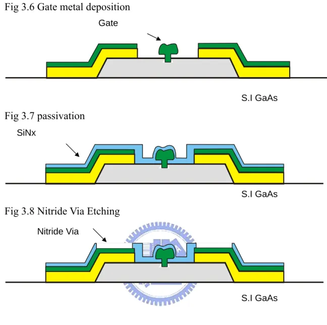
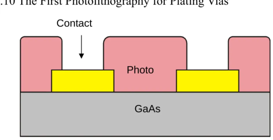
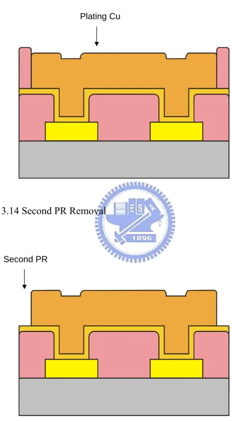
(10) Figures Fig 2.1 Schottky Contacts band diagram at different biases……………30 Fig 2.2 Physical image of the field emission and the tunneling at a Schottky junction……………………………………………....31 Fig.2.3 I-V characteristics of the Schottky diode......................………...31 Fig 3.1 MHEMT structure………………………………………………52 Fig 3.2 Mesa…………………………………………………………….53 Fig 3.3 Ohmic photo…………………………………………………….53 Fig 3.4 Ohmic metal…………………………………………………….53 Fig 3.5 Ohmic window and ebeam T-gate followed by recess………….53 Fig 3.6 Gate metal deposition………………………………………..…54 Fig 3.7 Passivation………………………………………………………54 Fig 3.8 Nitride Via Etching…...........……………………………………54 Fig 3.9 TLM of the AuGe/Ni/Au Ohmic contact for MHEMT………....55 Fig 3.10 the first photolithography for plating vias……………………..56 Fig 3.11 Thin metals Ti/Cu deposition………………………………….56 Fig 3.12 the second photolithography for plating areas………………...56 Fig 3.13 Cu electroplating………………………………………………57 Fig 3.14 Second PR removal……………………………………………57 Fig 3.15 Thin metal etching …………………………………………….58 Fig 3.16 Bridge passivation…..…………………………………………58 Fig 3.17 SEM of the Cu airbridges…………………………………..….59 Fig 3.18 (a) TLM pattern (b) The illustration of utilizing TLM to measure 10.
(11) the Ohmic contact resistance………………….……………..60 Fig 3.19 the equivalent two-port network schematic at high frequency...61. Fig 4.1 XRD spectra of Ti/Pt/Cu on i-InAlAs with different annealing temperature for 30 min.………………………………………..74 Fig 4.2 I-V characteristic of Ti/Pt/Cu diodes on i-InAlAs with different annealing temperature for 120 secs……………………………75 Fig 4.3 AES depth profiling of Ti/Pt/Cu on i-InAlAs (a) as deposited and annealed at (b) 350 ℃(c) 400 ℃ for 30 min.……………..…76 Fig 4.4 Cross-section of Ti/Pt/Cu on i-InAlAs after annealed at (a) 350 ℃(b) 400 ℃ for 30 min..………………………..……………77 Fig 4.5 EDX of Ti layer of Ti/Pt/Cu on i-InAlAs after annealed at (a) 350 ℃(b) 400 ℃ for 30 min..……………………………..………78 Fig 4.6 EDX of InAlAs layer of Ti/Pt/Cu on i-InAlAs after annealed at (a) 350 ℃(b) 400 ℃ for 30 min..………………………………..79 Fig 4.7 Barrier height varies with annealing temperature with three different pretreatments…………………………………………80 Fig 4.8 I-V characteristics of Ti/Pt/Cu gate copper-gate copper-airbridged LN MHEMT.........................................................................81 Fig 4.9 Transconductance vs. applied voltage Ti/Pt/Cu gate copper-airbridged LN MHEMT……..……………….…………81 Fig 4.10 Breakdown voltage Ti/Pt/Cu gate copper airbridged LN MHEMT…………………………………………….………..82 Fig 4.11 Drain I-V characteristics of Cu-airbridged LN-MHEMT 11.
(12) fabricated with Ti/Pt/Cu gate before and after 250°C 30mins thermal annealing in nitrogen atmosphere……………………83 Fig 4.12 Dependence of the transconductance on the gate bias voltage of Cu-airbridged LN-MHEMT fabricated with Ti/Pt/Cu gate before and after 250°C 30min thermal annealing in nitrogen atmosphere……………………………………………………83 Fig 4.13 Current gain cutoff frequency fT of Cu-airbridged LN-MHEMT fabricated with Ti/Pt/Cu gate…………………………....……..84. 12.
(13) Chapter 1 Introduction 1.1 Introduction MHEMTs and copper metallization process. Nowadays, much attention has been focused on the the InAlAs/InGaAs metaphoric high electron mobility transistors (MHEMTs). InAl0.52As/InGa0.52As heterostructures lattice-matched to InP can be grown on GaAs substrate using different designed buffer layers. Consequently, MHEMTs have outstanding high-frequency performances in terms of gain, noise figure, etc. They are of high technological interest for a wide variety of application including optical telecommunication, optical computing, and quantum electronics.. For GaAs and InP-based HEMT metallization process, gold plays an important role. Due to its high electrical conductivity and relative chemical inertness, gold is extensively used for GaAs device fabrication, like Schottky contacts (Ti/Pt/Au), Ohmic contacts (AuGe/Ni/Au), interconnect (Ti/Au), and so forth [1.1]. Notwithstanding gold is of very high cost for industry commercial use. Also for gold plating baths, the gold cyanide complex is harmful to the operator’s health.. Various materials can be used for the interconnect metallization. It was reported that gold and copper both have low resistivity (2.2 µΩ-cm for Au; 1.67µΩ-cm for Cu, table 1.1), and they provide high endurance 13.
(14) against electromigration resulting in failure[1.2]. Copper metallization has been extensively used in silicon integrated circuit technology since IBM first announced its success in realizing the silicon very-large-scale integration process [1.3-1.5]. The advantage of using copper metallization for Si technology include a low resistivity resulting in a lower RC delay, and potential enhancement in electromigration and stress resistance, which can improve the device performance [1.6].. Although the use of copper as the metallization metal instead of gold has become very popular in the fabrication of Si devices, copper diffuses very rapidly into Si when it is direct contact with Si substrate without any diffusion barrier. As in the case, copper also diffuses very rapidly into GaAs when it is direct contact with GaAs substrate without any diffusion barrier. If copper diffuses into the Ohmic contact, SiNx or active region of the device, it will result in the degradatinn of the electrical properties of the device.. Therefore, key issues need to be solved if Cu interconnections are used for GaAs device metallization:. (1) It is necessary to use a thin barrier layer to block Cu diffusion especially for narrow, high aspect-ratio structures.. (2) A passivation layer is required to prevent the oxidation of Cu surface [1.7].. 14.
(15) Above all, when it comes to Cu metallization for HEMT, we can use two kinds of metallization structures to fulfill Cu metallization process:. (1) Cu interconnects with diffusion barrier on Au-based electrodes (2) Fully copper metallization: Cu interconnects on Cu-based electrodes with diffusion barrier. In our prior work, our group had used WNx as the diffusion barrier, which was successfully applied to the Cu metallization of the airbridge, interconnects of the AlGaAs/InGaAs low noise pseudomorphic HEMTs to prevent interconnection metal Cu from diffusing into gate and Ohmic metal underneath. The copper plating bath was a copper sulfate based solution (CuSO4.5H2O), and it may be recycled. It is less detrimental to the environment than the gold bath. Moreover WNx was found to have poor adhesion onto metal contacts, for that reason, Ti was introduced in between to WNx and Copper to preventing peeling .. In this work, copper replaced gold as the top gate metal, traditional Ti/Pt/Au gate structure was substituted by Ti/Pt/Cu for the copper metallization process of the MHEMTs. Pt is an effective diffusion barrier for Cu and id thermally stable up to 350 ℃ annealing, and shows similar characteristics compared to the Ti/Pt/Au gate metal. This metal system was also deposited onto Ge-based metals to form Ohmic contact on highly doped InGaAs cap layer. And the thin metal was simplified as Ti/Cu for Cu airbridge interconnects. And plasma-enhanced chemical 15.
(16) vapor deposition (PECVD) silicon nitride film was deposited after copper airbridge fabrication to prevent copper surface from oxidation. The goal of the study is to build a simple and convenient Cu metallization process for MHEMTs in order to reduce the production cost of manufacture of the GaAs devices and to provide comparable or even better thermal and electrical device performance.. 1.2 Thesis content. The copper metallization process for GaAs MHEMTs is outlined in introduction. In this thesis, both copper contacts and copper interconnects are arranged in parallel to fulfill the copper metallization for MHEMTs.. In chapter 2, the basic theory and the paper review of the Schottky contacts were presented. The material analysis and the characteristics of the Ti/Pt/Cu Schottky diodes on undoped InAlAs were shown in chapter 4. The samples were subjected to thermal treatments to examine their thermal stability. Material analysis was for the comprehensive study of the stability of the Ti/Pt/Cu structure.. A full and accurate description is given for the copper metallization process in chapter 3. Furthermore, the process flow will be compared to that of the Au metallization process for etch step.. In chapter 4, the Ti/Pt/Cu gate metal system was applied to fabricate high-performance MHEMTs. The DC, RF, noise figure and power 16.
(17) performance MHEMT devices of the MHEMTs will be demonstrated. Then, in the final chapter, we will summarize and conclude the experiment results in this study. Some suggestions for future studies will also be given for the improvement of the Cu metallization process.. 17.
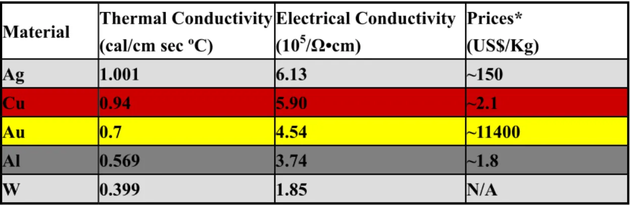
(18) Table 1.1 Comparison of the properties and price for different metals Material. Thermal Conductivity Electrical Conductivity Prices* (cal/cm sec ºC) (105/Ω•cm) (US$/Kg). Ag. 1.001. 6.13. ~150. Cu. 0.94. 5.90. ~2.1. Au. 0.7. 4.54. ~11400. Al. 0.569. 3.74. ~1.8. W. 0.399. 1.85. N/A. 18.
(19) Chapter 2 Study of Schottky contacts on InAlAs. The ternary compound InxAl1-xAs is an important wide-band-gap semiconductor material (1.436 eV) used in high-electron mobility transistors (HEMTs) and optoelectronic devices. It is evident that although relatively high barrier is achievable for InAlAs, they may be disparity between the measured results. The measured barrier height depends on the characterization techniques used, the InAlAs epitaxial grown and the quality of the semiconductor surface [2.1-2.3], and the contact metal used (shown as table 2.1).. 2.1 Theory of Schottky Contacts. When metal is making intimate contact with a semiconductor, the Fermi levels in the two materials must be coincident at thermal equilibrium. This can be achieved through a charge flow from semiconductor to metal. Thus a barrier forms at the interface and an equal and opposite space charge is contributed over the barrier region near the. 19.
(20) semiconductor surface. With an n-type semiconductor in the absence of the surface state, the barrier height qψbn is given by:. qψbn=q(φm-χ). Where qψbn is the metal work function, qχ is the electron affinity of semiconductor. For an ideal contact between metal and a p-type semiconductor, the barrier height qψbn is given by:. qψbp=εg- q(φm-χ). When surface states are present on the semiconductor surface, and the density is sufficiently large to accommodate any additional surface charges without appreciably altering the occupation level Ef, the space charge in semiconductor will remain unaffected. As a result, the barrier height is determined by the properties of the semiconductor surface, and is independent of the metal work function. In practice, some surface states always present at semiconductor surface, and energies continuously distributed within the energy gap. The Schottky barrier. 20.
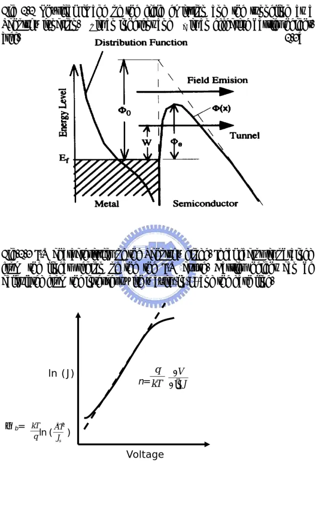
(21) heights of the metal-semiconductor systems with intimate contact are, in general, determined by both the metal work function and the surface states.. The current transport the in metal-semiconductor contacts is mainly due to the majority carriers, in contrast to the p-n junctions. Two major processes under forward bias, and based on the diffusion theory of Wagner (1931) and Mott (1939), and the thermionic emission theory of Bethe (1942). A good combination of the two theories is achieved by Henisch (1957).. (1) Field emission / Thermionic emission: transport of the electrons from the semiconductor over the potential barrier into the metal; (2) Tunneling / diffusion: quantum-mechanical tunneling of electrons through the barrier.. According. to. the. diffusion,. the. current. flowing. in. a. metal-semiconductor barrier is supposed to be determined by the process of diffusion and drift operating in the space-charge region, as shown in. 21.
(22) Fig. 2.2, while the Thermionic emission theory, the current is determined by the emission of electrons from the semiconductor over the top of the barrier into the metal.. In addition, we may have recombination current in the space –charge region and leakage current at the contact periphery. The effect of tunneling on breakdown of Schottky gate of InAlAs/InGaAs HEMTs was reported and explained that their low breakdown voltages are attribute to tunneling effect. The transport of the electrons over the potential barrier is often the dominant process for Schottky diodes on the moderately doped semiconductors. It can be adequately described by the thermonic emission theory for the high mobility semiconductor (for low mobility materials, the diffusion theory is also appreciable), and the electric current density over the barrier has the following expression:. J=Js [exp (. qϕ qV qV )-1] = A**T2exp (- b ) [exp ( )-1] kT kT kT. Where Js is the saturation current density, A** is the effective Richardson constant. In practical device, the barrier height dependent on. 22.
(23) bias voltage and the current-voltage characteristics is more accurately described by:. J=A exp (-. qϕ b qV ) [exp ( )-1] kT nkT. Factor n is called the ideality factor. The barrier height and ideality factor can be obtained from the forward J-V characteristics (for V > 3kT/q) in fig 2.3, and. n=. ψb =. q ∂V kT ∂ ln J. kT A**T 2 in( ) q Js. For a heavily doped semiconductor or for operation at high temperatures, the tunneling current may become the dominant transport process. The tunneling current has an expression:. 2ϕ b Jt ~exp ( h. ε s m* ND. ) 23.
(24) Where εs is permittivity of the semiconductor; m** is effective mass of carrier, Nd is carrier concentration. It indicates the current will increase exponentially with Nd1/2.. 2.2 Gate Formation. The Schottky barrier gate is one of the most important elements of GaAs devices. The gate metal used, the gate length are critical to the performances of both power and low noise HEMTs. Uniformity of the device performance is also resulted from reproducible fabrication process. Generally, a high barrier height of the gate in drive threshold is increased when the barrier height of the gate contact is increased. Also a higher reverse breakdown of the Schottky contact is very beneficial for power device application. Although almost any metal placed on GaAs will yield a Schottky barrier, the metal must also exhibit two other characteristics: good adhesion and thermal stability. Gold is one of the choices for both advantages, but it shows poor adhesion and is highly susceptible to diffusion. A good adhesion layer and an excellent diffusion barrier are. 24.
(25) needed for gold to be gate material. Titanium is ideal for adhesion layer and the barrier metal is usually platinum. Adhesion of Ti was observed to be good, scratching by probe needles can does not remove the metal contacts. In this case, barrier metals which prevent diffusion are used between the Schottky contact metal and the gold. Other structures such as TiMoAu, CrPdAu, and MoAl have also been used for Schottky contacts.. The Ti/Pt/Au Schottky contacts using Ti as the Schottky barrier metal is the most important multilayer metallization system because of its wild use in the fabrication of metal semiconductor field effect transistors, high electron-mobility transistors, and Schottky barrier diodes. Table 2.1 shows several common Schottky metal structures on InAlAs and the Schottky characteristics.. Besides the main concern of appropriate gate metal for III-V compounds, there are other things need to be taken into consideration. The electrical properties of the Schottky contact are strongly dependent on the defects in the material. With the help of molecular beam epitaxy, one may have epitaxy wafer with good quality. The high resistivity of the. 25.
(26) low temperature grown InAlAs is usually ascribed to the appearance of new defects caused by the low growth temperature which pin the Fermi level near mid-gap. [2.5] These defects act as traps distributed within the layers and also a transition step for reverse bias defect-assisted tunneling current.. On the other hand, the surface pretreatment on the characteristics of the Schottky diodes fabricated on InAlAs has been an important issue for MESFET and HEMT process. The characteristics of the Schottky diodes formed were fairly sensitive to the etching conditions used, indicating the importance of the state of the surface and its native oxide prior to the barrier formation. As shown in former researches, the best enchants led to systematic increase in ψbn by 0.05 eV from the average value pounced by using the worst enchants investigated. [2.7]. Moreover, there are a number of reports suggested that the physical structure of a real Schottky barrier is far more complicated than of an ideal planar junction between the semiconductor and metal. It is generally realized that defects at or near the surface of a semiconductor are playing. 26.
(27) an important role in the formation of Schottky barrier and can dominate the electrical properties of Schottky barriers. Although the Schottky diode is one of the most elementary electronic devices, and large effort has been devoted to the study of the metal-semiconductor junction, it is clear that both the physical and electrical properties of this device are not completely understood.. 2.3 Ti/Pt/Cu Schottky structure. Ti/Pt/Au is the most widely used metal structure for the fabrication of Schottky contacts in MESFETs, HEMTs, and Schottky diodes. In this study, one brand new Cu-metallized gate metal structure was proposed for MHEMTs, the top Au layer of the Schottky structure was replaced by Cu. This is due to Cu has the advantages of reduced electrical resistivity and production cost compared with the use of Au for metallization process. The Ti/Pt/Cu gate was formed on the undoped InAlAs layer. Ti acts as Schottky metal with good adhesion on the semiconductor surface. The Pt layer in Ti/Pt/Au structure was used as diffusion barrier due to its excellent anti-diffusion capability and the electrical conductivity. The. 27.
(28) effect of using different pretreatment was also included in this study. The interface of metal-semiconductor contact will be fully examined by XRD, AES, and TEM.. 28.
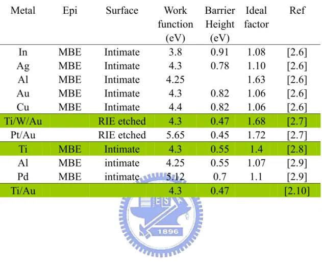
(29) Table 2.1 Paper review on various Schottky diodes on InAlAs using different Metal system. Metal. Epi. Surface. In Ag Al Au Cu Ti/W/Au Pt/Au Ti Al Pd Ti/Au. MBE MBE MBE MBE MBE. Intimate Intimate Intimate Intimate Intimate RIE etched RIE etched Intimate intimate intimate. MBE MBE MBE. Work function (eV) 3.8 4.3 4.25 4.3 4.4 4.3 5.65 4.3 4.25 5.12 4.3. 29. Barrier Ideal Height factor (eV) 0.91 1.08 0.78 1.10 1.63 0.82 1.06 0.82 1.06 0.47 1.68 0.45 1.72 0.55 1.4 0.55 1.07 0.7 1.1 0.47. Ref. [2.6] [2.6] [2.6] [2.6] [2.6] [2.7] [2.7] [2.8] [2.9] [2.9] [2.10].
(30) Fig 2.1 Schottky Contact band diagram at different bias conditions. (a) Before contact. (b) at thermal equilibrium. (c) Reverse bias. (d) Forward bias. 30.
(31) Fig 2.2 Physical image of the field emission and the tunneling at a Schottky junction. Φo is an inherent and Φc is an effective barrier height. [ref. 2.3]. Fig.2.3 I-V characteristics of the Schottky diode. Ideal factor is obtained from the linear region of the the I-V curve. Barrier height can be calculated from the intercept with y axis (ln(J))and the dash line.. ln (J). ψb= kT. q ∂V n= kT ∂ ln J. ** 2 AT. q ln ( Js ). Voltage. 31.
(32) Chapter 3 Device Process and Measurement 3.1 Device structure. The epitaxial layers of the metamorphic HEMT with InxAl1-xAs grading buffer layer were grown by molecular beam epitaxy (MBE). The cross-section of the MHEMT structure is shown in Fig. 3.1. The Indium graded InxAl1-xAs metamorphic buffer layer was grown on a 3-inch semi-insulating GaAs wafer, followed by an undoped In0.52Al0.48As buffer layer. 15 nm In0.52Ga0.48As was chosen as the channel layer. The Si-planar doping (2x1012 cm-2) layers were separated from the channel layer by 4 nm thin undoped In0.52Al0.48As spacer. The undoped In0.52Al0.48As Schottky layer was 15 nm. Then, the 18 nm thick In0.52Ga0.48As cap layer was highly doped with Si of 2x1018 cm-3 for Ohmic contact formation.. 3.2 Ti/Pt/Cu Schottky diode sample preparation. The InGaAs/InAlAs samples used in this study were grown by MBE. The structure of the samples consists of a 30 nm Si-doped n-InGaAs top of a 150 Å InAlAs Schottky layer on the GaAs substrate. The samples were first cleaned with acetone and isopropyl alcohol for 5 min, followed 32.
(33) by dipping in HCl: H20 (1:10) solution for 3 min. The samples were then immediately put into an electron-beam evaporating system and pumped down to a pressure of 8 × 10⁻⁷ Torr. Rectangular contact pads of Au/Ge/Ni/Au multilayer metals were evaporated on n-InGaAs and were RTA annealed at 320℃ for 20 s in nitrogen gas to form Ohmic contacts. The. Schottky. contact. materials,. Ti/Pt/Cu. were. deposited. by. electron-beam evaporating system after InGaAs cap layer was etched. Ti/Pt/Cu was also deposited on InAlAs wafer for material analysis. And different pretreatments were performed by HCl dipping, NH4OH dipping and N2 etching before Schottky metal deposition. The final thickness of these films was about 4000 Å. The diameter of the Schottky pattern was 1.23 mm. The current-voltage (I-V) characteristics of the as-deposited and annealed diodes were measured at room temperature using a HP4145B semiconductor parameter analyzer.. 3.3 Device Fabrication. The fabrication process of the MHEMTs in this study includes:. 1. Mesa/device isolation 33.
(34) 2. Ohmic contact formation 3. Gate formation 4. Device passivation 5. Airbridge formation. The detail will be described in the following sections.. 3.3.1 Mesa isolation. Device isolation is the very first step of the whole HEMT fabrication process which was used to define the active region on the wafer. In these defined areas by lithography technique, the current flow is restricted to the desired path and each active device is isolated from each other (Fig 3.2). There are three typical ways to achieve device isolation: wet etching, ion bombardment, and selective implantation. Wet etching is the simplest way of the three. In this study Mesa isolation was carried out by a phosphoric based solution. The active areas were masked by Shipley S1818 photo resist. According to the device structure, the inactive era was etched to the buffer layer to provide good isolation. In order to avoid the photo resist peeling during the etching, the wafer surface was pre-treated before resist coating by Hexamethyldisilazane (HMDS). Finally, the etching depth was measured by α-step or surface profiler after the photo-resist was stripped and the etched profile was checked by Scanning electron microscopy (SEM). To inspect the mesa isolation process, a test pattern with a 10µm gap is used to measure the leakage current.. 34.
(35) 3.3.2 Ohmic contact Formation. After wafer cleaning by using ACE and IPA, the negative photo resist and I-line aligner were used to define the Ohmic pattern and make sure to form undercut profile for the metal lift-off (Fig 3.3). Ohmic metals multilayer Au/Ge/Ni/Au, from the bottom to the top, was deposited in the appropriate composition by e-gun evaporation system. After lift-off process, source and drain Ohmic contacts were formed after 320℃ for 20 sec in nitrogen atmosphere (Fig 3.4). Germanium atoms diffused into the InGaAs and heavily doped InGaAs during the thermal annealing process. The specific contact resistance was checked by the transmission line method (TLM) in the process control pattern monitor (PCM). The typical measured contact resistance was < 1 x 10⁻⁶ Ω-cm2 (Fig. 3.9).. 3.3.3 T-shaped gate process. For high frequency and high speed application, short gate length with low gate resistance is expected. T-shaped gate structure was the most common approach for obtaining low gate resistance. According to the T-gate structure design, the gate length is defined by small footprint and the wide top offers low gate resistance.. T-shaped gates were achieved by using a multilayer resist technique with E-beam lithography. In this study, PMMA/copolymer was used as the resist system to form the T-shaped gates. The fabricated PHEMT in 35.
(36) this study has a gate length of 0.2µm.. Before T-gate lithography, in this study, Ohmic areas were exposed by optical lithography (Fig 3.5). Not only for gate metal, was Ti/Pt/Cu metal was also deposited on this area for Cu interconnect fabrication. Pt was effective diffusion barrier to keep Cu diffusion into the underlying Au layer.. After patterning the T-shaped gate, the exposed HEMT channel was recessed to achieve the desired channel current and pinch-off voltage characteristics. That means a groove is fabricated in the exposed surface of the wafer to “recess” the gate. This process is done by wet etch technique in this study, although dry etching methods may also be used. The recess etching was conducted using PH-adjusted solution of succinic (S.A.) and H2O2 mixture to perform selective etching of the heavily doped InGaAs cap layer over InAlAs Schottky layer. The concentration of the etchant should be adjusted to provide an etch rate that is sufficiently slow to allow good control over the recess process, thus enable the operation to approach the target current value, without over etching it. The etching selectivity of InGaAs cap layer over InAlAs Schottky layer was beyond 100.The schematic of the HEMT with recessed gate is as shown in Figure 3.5, too.. The target current after the gate recess is a critical parameter affecting the HEMT performance. In order to get the desired recess depth, the recess process was controlled by monitoring the ungated Ids. The 36.
(37) method used to control the recess depth is to monitor the source-to-drain current during the etching process. For low noise PHEMT, the saturation current and the slope of the linear region go down as the recess groove was etched deeper and deeper. The wet etchant usually leaves a thin oxide on the InAlAs. HCl-based solution was used to remove the surface oxide. After recess etching, Ti/Pt/Cu gate metal was evaporated and lifted off.. 3.3.5 Device passivation and contact via formation. FETs are very susceptible to the surface condition, especially in the gate region. As the device scales down, the gate length and spaces of source-to-drain and gate-to-drain become smaller. In situation like this, the devices are very sensitive to the damages and contaminations such as chemicals, gases, and particles. The passivation layer protects the device from damage during process handling (such as “airbridge”) and wafer probing (Fig 3.7). The dielectric layer SiNx is a common choice for device passivation.. In this study, Samco PECVD system was used for depositing silicon nitride film. The processing gases of passivation PECVD were Silane, ammonia, and nitrogen. The process condition is: process pressure: 100Pa, process temperature: 300 °C and process time: 10 minutes to form the silicon nitride film 1000Å. The reflection index was inspected by Ellipsometer about 2.0.. Then the contact openings of the devices were formed by photo 37.
(38) lithography (Fig 3.8). The RIE was used to open the contact via hole region of the source and drain pads for interconnection. The plasma gases source for SiNx etching were mixture of CF4 and O2.. 3.3.6 Airbridge formation. In order to reduce the total device area, finger-type layout was adopted. As a result, airbridge process was necessary to contact the fingers. The use of airbridge had several advantages including lowest dielectric constant of air, low parasitic capacitance, and the ability to carry substantial currents. The airbridge process flow will be discussed in detail in next section.. 3.4 Airbridge formation Airbridge is built by metal with air between the metal interconnect and the wafer surface beneath. Airbridges are used extensively in GaAs analog devices and MMICs for interconnections [3.1]. They may be used to interconnect sources of FETs, to cross over a lower level of metallization, or to connect the top plate of a MIM capacitor to adjacent metallization. The airbridges have several advantages including low parasitic capacitance, and the ability to carry substantial currents if the plated airbridge is thick enough. Analog GaAs devices operating at high current density benefit from airbridges with thick plated metal layer. Low parasitic capacitance (between the bridge and any metallization beneath) follows from the large 38.
(39) spacing and low dielectric constant of the intervening medium. The capacitance is a function of the thickness, and the dielectric constant of the intervening material. Air (k=1.0) has a much lower dielectric constant than any other dielectric, and the space under the airbridge tends to be greater than the thickness of typical dielectrics. These considerations mean that airbridge crossovers are less capacitive than the dielectric type by a factor (typically) of five to twenty. Traditionally, Au is used as the interconnect metal in III-V device fabrications, mainly owing to its high electrical conductivity and better chemical inertness with no surface oxidation. Recently Cu has been used widely in Si IC interconnects due to its low resistivity and high electromigration resistance. Both the resistivity and the material cost of Cu (1.67 µΩ-cm) are lower than those of Au (2.2 µΩ-cm). Based on the above advantages, Cu was used instead of Au as the airbridge metal in order to provide better thermal and electrical conductivities for the device applications.. 3.4.1 Comparison between Au airbridge and Cu airbridge processes. The following process flow was used to fabricate the airbridge interconnects.. 1. The first photolithography for plating vias 2. Thin metals deposition 3. The second photolithography for plating Areas. 4. Electroplating.. 39.
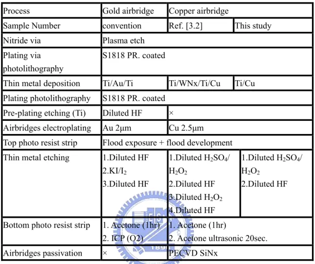
(40) 5. Second PR removal and thin metal etching. 6. First PR removal 7. Bridge Passivation. (For copper metallized airbridge only). Table 3.1 shows the process flow of one conventional Au and two Cu-airbridge formation methods. There are three main differences between the fabrications of the Au airbridges and Cu airbridges: thin metal structure, electroplating and airbridge passivation.. Au airbridge used Ti/Au/Ti as thin metal while Ti/WNx/Ti/Cu was used in Ref [3.2] and Ti/Cu was used in this work for Cu airbridge. Among the three airbridge processes, pre-plating etching was eliminated for the two Cu airbridge processes. Besides, compared to Au airbridge and Cu airbridge process in Ref [3.2], the selectively thin metal etching of the proposed Cu-airbridge process in this study was simplified as well. For Au airbridge, Ti/Au/Ti metal system is chosen for thin metal. In Ref [3.2], Ti/WNx/Ti/Cu was their choice of thin metal. WNx was the diffusion barrier for Cu and the Au contacts (Ohmic and gate top metal). In this study, the top metals of Ohmic and gate are both copper-based structure with diffusion barrier, so the thin metal structure was simplified to Ti/Cu without the worries of the diffusion between Au-based contacts and Cu interconnects. Moreover the Ti/Cu thin metal needed no additional layer of Ti to improve the adhesion in between seed metal and second photo resist. As for thin metal etching, the process was simplified as well because the simpler thin metal system. Finally the passivation of SiNx was used for preventing Cu oxidation in atmosphere. 40.
(41) The Cu airbridge process in this study will be expounded in detail in the next section.. 3.4.2 The First Photolithography for Plating Vias. The thickness of the first layer of resist determines the spacing between the bridge and the material beneath (usually a dielectric). The thickness of the photo resist was about 2.5 µm. (Fig 3.10). After the wafer was immersed in Acetone (ACE) and isopropyl alcohol (IPA) for 5 minutes, and dried by compressed dried air (CDA) blowing, the first layer of photo resist lithography was performed. The thickness was about 2.5 µm. In order to remove the thin PR residues in the exposed region, an O2 descum process was necessary after the photolithography. Then the wafer was plate-baked immediately after the ICP descum. This bake was used to evaporate the remaining solvent in the photo resist. On the other hand, the first photo resist must be sufficiently baked to prevent the “bubbling” after thin metal deposition and the later thermal bake of the second photolithography.. 3.4.3 Thin Metal Deposition for Cu airbridges. The thin metal structure of the copper airbridge was Ti/Cu with Ti as the adhesion layers. The thicknesses of these two metal layers were 300 Å, and 1000 Å, respectively, from the bottom to the top. (Fig 3.11) 41.
(42) 3.4.4 The Second Photolithography for Plating Areas. The second photolithography was performed on thin multilayer metals. The thickness of the second PR was about 2.5 µm. Same as the first lithography, descum is necessary to remove the polymer residues after development. (Fig 3.12). 3.4.5 Copper Electroplating. The wafer was cleaned before plating to prevent contamination. The wafer was dipped in the diluted sulfuric acid to remove the surface copper oxide. However, the sulfuric acid also attacks copper and the dipping time should not be too long. The wafer was dipped in the diluted sulfuric acid (1:10) for 5 seconds. The current density of the copper electroplating was 1 A/dm2 and the plating time was 10 minutes for 2.5 µm thick copper. (Fig 3.13). 3.4.6 Plating PR. Removal and the Thin Metal Etching. The samples after electroplating were immersed in ACE to remove the second photo resist of the airbridges. (Fig 3.14) The thin metals used for the Cu airbridges were Ti/Cu. The wafer was dipped in the diluted sulfuric acid (1:10) for 5 seconds to remove the surface copper oxide. The thin copper metal was then etched by H2SO4/H2O2/H2O solution mixed in the volume ratio of 5:6:100. The etching rate of this step is very high, and 42.
(43) the etching of copper stops at the underlying Ti as the color turned from red to grey.. Titanium was also etched by mixed 1:100 HF (49 %): H2O solution. HF is the active ingredient in this etchant, so it also etches oxides. Raising the fraction of HF in the solution increases the etching rate. Titanium is readily oxidized, so it is likely to form an oxide layer from the water, which is readily etched by the HF in this solution, resulting in the formation of bubbles of oxygen. (Fig 3.15). 3.4.7 The First PR. (bottom layer) Removal. For copper airbridges, however, the PR residues were stripped by ultrasonic ACE bath instead of O2 plasma to prevent copper contamination of the ICP etcher.. For copper-metallized airbridges, the samples were dipped in ACE for 20 minutes to remove the first photo resist for plating vias. And then the specimens were dipped in IPA for 2 min. They were finally immersed in D.I. water, and then followed by CDA drying (Fig 3.16).. 3.4.8 Airbridges Passivation. Silicon nitride was used as the passivation layer for copper airbridges to prevent surface oxidation. This dielectric passivation was deposited by plasma enhanced chemical vapor deposition (PECVD) 43.
(44) method. The SEM photograph of the copper airbridge with silicon nitride passivation is shown in Figure 3.17.. 3.5 DC Characteristics. 3.5.1 DC measurement. Keithley 2400 source meter, HP 4141B, and Karl Suss semi-automatic probe system was set up to measure the DC characteristics of the devices.. (1) I-V characteristics. In this experiment, the drain-to-source voltage was applied from 0 to 2 volts. The gate- to-source voltage range from 0 to -1.5 volts for low noise MHEMTs.. (2) Transconductance Gm. The drain-to-source voltage is biased at 1.5 volts and the gate-to-source voltage varies from 1.5 to -3 volts for GaAs low noise MHEMTs. The value of Gm was calculated by differentiating Id vs. Vgs curve. 3.5.2 Transmission line model (TLM) [3.3] 44.
(45) The resistance of the ideal planar contacts may be found using a transmission-line method (TLM). This technique is based on the assumption that specific contact resistance is determined by either the metal-semiconductor interface or by the interface between the alloyed and nonalloyed portions of the active layer, and the semiconductor resistivity under the contacts is uniform (through it may be different from that outside the contact). The typical TLM pattern used for the measurements is shown in Fig. 3.18 (a). The resistance between two adjacent pads of width W and length d separated by distance L is given by:. R=RsL/W+ 2Rc. Where Rs is the sheet resistance of the active layer between the contacts (i.e. the film resistance per square), Rs is the contact resistance. The values of Rc and Rs were determined from the intercept and the slope of the R vs. L curve, as shown in Fig. 3.18 (b).. 3.5.3 Breakdown characteristics [3.4]. Breakdown mechanisms and models are discussed in many articles. One of them shows it is dominated by the thermionic field emission (TFE) / tunneling current in the Schottky gate contact area. Tunneling currents are known to increase with the temperature rising because the carriers 45.
(46) have higher energy to overcome the Schottky barrier which makes, according to this model, two-terminal breakdown voltage lower at higher temperature. Other model suggests the final two-terminal breakdown voltage is determined by impact-ionization determines, because the avalanche current decreases with increasing temperature. Lower avalanche current occurs at higher temperature because the phonon vibrations as well as carrier-carrier scattering increase with the increasing temperature.. As so far, breakdown mechanisms are still complicated to define clearly. Either model mentioned above is incomplete since coupling exists between TFE and impact ionization mechanisms. In addition, different devices may suffer from different breakdown mechanisms, depending on the details of the device design (insulator thickness, recess, channel composition, and so on). In this study, the gate-to-drain breakdown voltage is defined as the gate-to-drain voltage when the gate current is 1mA/mm. 3.6 RF Characteristics& Measurements 3.6.1 Scattering parameters [3.5] Scattering parameters, generally referred to as S-parameters, are fundamental to microwave measurement. The scattering parameters are used to characterize the performance of a device. Figure 3.15 shows the two-ports 1 and 2.When the frequency is up to several GHz, the z-, y-, hparameters can not be directly obtained by the open or short circuit 46.
(47) because of the reflected wave from the open or short terminations. The open or short terminations will induce the network oscillation. The relation of the microwave signals and s-parameters can be described as. S-parameters:. ⎡ b1 ⎤ ⎡ s11 ⎢ ⎥=⎢ ⎣ b 2 ⎦ ⎣ s 21. s12 ⎤ ⎡ a 1 ⎤ ⎥*⎢ ⎥ s 22 ⎦ ⎣ a 2 ⎦. a1: the electric field of the microwave signal entering the component input b1: the electric field of the microwave signal leaving the component input a2: the electric field of the microwave signal entering the component output b2: the electric field of the microwave signal leaving the component output. By the definition, then,. s11 =. b1 a1 a 2 = 0. s 21 =. b2 a1 a 2 = 0. s12 =. b1 a 2 a1 = 0. s 22 =. b2 a 2 a1 = 0. 47.
(48) Therefore, S11 is the electric field leaving the input divided by the electric field entering the input, under the condition that no signal enters the output. The measurement includes instruments for the DC and RF measurement. Where a1and b1 are electric fields, their ratio is a reflection coefficient. Similarly, S21 is the electric field leaving the output divided by the electric field entering the input, when no signal enters the output. Therefore, S21 is a transmission coefficient and is related to the insertion loss or the gain of the device. Similarly, S21 is a transmission coefficient related to the isolation of the device and specifies how much power leaks back through the device in the wrong direction. S22 is similar to S11, but looks in the other direction into the device. The s-parameters have both the amplitude and phase. 3.5.2 Current gain cutoff frequency fT and maximum frequency of oscillation fmax [3.6]. fT is defines as the frequency when current gain equals unit, and can be express as:. fT ≈. gm Vsat 1 ≈ ∝ 2π (Cgs + Cgd ) 2π Lg ( eff ) Lg. fmax can be obtained by using unilateral gain:. U = Gu max = (1/4) (fT2/f2)(1/RiGd). 48.
(49) When U =1, fmax can be expressed as:. f. max. ≈. fT CMiller ⎞ ⎛ 2 ( Rg + Rs + Ri )⎜ gd + gm ⎟ Cgin ⎠ ⎝. fT and fmax are parameters often used to indicate the high frequency capability of the transistors.. 3.6.3 Noise figure [3.7]. In wireless communication, the generation of noise has notorious impact on the quality of the signal transmission. There are many different types of noise generation, two most influential are thermal noise and shot noise. Noise figure reflects the noise added to the signal by the imperfect amplifier, and is defined as the signal-to-noise ratio (S/N) of the input signal divided by the signal-to-noise ratio of the output signal,. F = (Si/Ni)/ (S0/F0). It is usually expressed in dB:. NF = 10logF. Another noise figure of FETs structure is shown as the following equation.. 49.
(50) NF = 1 + 2. f ft. g m (R s + R g) , f t =. gm. 2π C gs. In general, high source-drain current contributes to noise by electron scattering, and this noise is reduced as the current is reduced. However, reducing the current too close to pinch-off reduces the transconductance, which causes increased noise figure because of decrease gain. There will exist an optimum gate bias that presents the best compromise.. 50.
(51) Table 3.1 Comparison of Au and Cu airbridges Process. Gold airbridge. Copper airbridge. Sample Number. convention. Ref. [3.2]. This study. Nitride via. Plasma etch. Plating via photolithography. S1818 PR. coated. Thin metal deposition. Ti/Au/Ti. Ti/WNx/Ti/Cu. Ti/Cu. Plating photolithography. S1818 PR. coated. Pre-plating etching (Ti). Diluted HF. ×. Airbridges electroplating. Au 2µm. Cu 2.5µm. Top photo resist strip. Flood exposure + flood development. Thin metal etching. 1.Diluted HF. 1.Diluted H2SO4/. 1.Diluted H2SO4/. 2.KI/I2 3.Diluted HF. H2O2 2.Diluted HF 3.Diluted H2O2 4.Diluted HF. H2O2 2.Diluted HF. Bottom photo resist strip. 1. Acetone (1hr) 2. ICP (O2). 1. Acetone (1hr) 2. Acetone ultrasonic 20sec.. Airbridges passivation. ×. PECVD SiNx. 51.
(52) Fig 3.1 MHEMT structure. n+ -In0.52Ga0.48As Cap layer i-In0.52Al.0.48As Schottky. Si planar-doping 2x1012cm-3. i-In0.52Al.0.48As Spacer i-In0.52Ga0.48As Channel i-In0.52Al0.48As InAlAs buffer Composition Grading Layer S.I. GaAs Substrate. 52.
(53) Fig 3.2 Mesa Photo Resist. S.I GaAs. Fig 3.3 Ohmic photo Photo Resist. S.I GaAs. Fig 3.4 Ohmic metal AuGe/Ni/Au. S.I GaAs. Fig 3.5 Ohmic window and ebeam T-gate followed by recess Photo resist PMMA/Coplymer. S.I GaAs. 53.
(54) Fig 3.6 Gate metal deposition Gate. S.I GaAs. Fig 3.7 passivation SiNx. S.I GaAs. Fig 3.8 Nitride Via Etching Nitride Via. S.I GaAs. 54.
(55) Fig 3.9 TLM of the AuGe/Ni/Au Ohmic contact for MHEMT. SPACE(mm). 3. 5. 10. 20. 36. 1. 6.523. 8.882. 15.753. 28.659. 50.213. 2. 6.872. 9.001. 15.972. 29.123. 51.345. Orange line (W/[])=. 9.8081E+01. Blue line (W/[])=. 1.0010E+02. Orange line rC(W-cm2)=. 8.7722E-07. Blue line rC(W-cm2)=. 9.0565E-07. 60. 50. 數列1. 數列2. Resistance(( Ω ). 40. 數列3 數列4 數列5. 30. 數列6 數列7. 20. 數列8 數列9. 10. 0 0. 10. 20 W idth(µm). 55. 30. 40.
(56) Fig 3.10 The First Photolithography for Plating Vias Contact. Photo. GaAs. Fig 3.11 Thin Metals Ti/Cu Deposition.. Thin Metal Ti/Cu. Fig 3.12 The Second Photolithography for Plating Areas.. Photo resist. 56.
(57) Fig 3.13 Cu electroplating.. Plating Cu. Fig 3.14 Second PR Removal. Second PR. 57.
(58) Fig 3.15 Thin Metal Etching.. Thin Metal etching. Fig 3.16 First PR Removal. First PR. removal. Air Bridge. Air. 58.
(59) Fig 3.17 SEM of the Cu airbridges (a) plan view for 40µmx4. (b) side view. 59.
(60) Fig 3.18 (a) The TLM pattern. (b) The illustration of utilizing TLM to measure the Ohmic contact. resistance. 60.
(61) Fig 3.19 The equivalent two-port network schematic at high frequency. 61.
(62) Chapter 4 Results and Discussion. In the first part of this chapter, Ti/Pt/Cu Schottky structure was studied and compared with the traditionally Ti/Pt/Au Schottky. The Ti/Pt/Cu structure was characterized by XRD, AES, TEM and I-V measurement to evaluate the effectiveness of Pt as a diffusion barrier for Cu. And three different pretreatments were conducted to remove the surface oxide of InAlAs after recess etching. The Ti/Pt/Cu Schottky characteristics were also presented in this section.. 4.1 Characteristics and material analysis of the Ti/Pt/Cu Schottky diodes on InAlAs. 4.1.1 XRD. Fig 4.1 shows the X-ray diffraction (XRD) patterns of the Ti/Pt/Cu multilayer metals on InAlAs. To investigate the diffusion barrier property of platinum for Ti/Pt/Cu gate structure, the Ti/Pt/Cu films were first. 62.
(63) evaporated on an InAlAs using e-gun evaporator and subjected to anneal for 30 min at different temperatures in nitrogen ambient for material analysis. Fig 4.1 also shows the XRD results of the Ti/Pt/Cu samples as-deposited and after annealed from 300℃ to 400℃ for 30 min. XRD was mainly used to monitor the interfacial reactions. From this evidence revealed by XRD, the Ti/Pt/Cu/InAlAs structure was stable up to 350 ℃ annealing. In the XRD figure the peaks of Cu, Pt, and Ti remained unchanged and kept distinct shape up to 350 ℃ annealing, that is ,the Ti/Pt/Cu structure were quite stable up to 350 ℃. However, after 400℃ annealing, Cu was found diffusing through Pt and reacted with the Ti metal, meanwhile additional peaks emerged. The intermetallic compound peaks were identified as Cu4Ti. Besides, the Cu4Ti diffraction peaks appeared and the Ti and Pt peaks disappeared. Owing to the inter-diffusion of the atoms, the Ti and Pt layer disappeared. The Ti layer and Pt layer vanished after the inter-diffusion and resulted in the weakening signal of the Ti and Pt peaks. The formation of Cu4Ti after 400 ℃ annealing suggested that Cu atoms had diffused through the Pt layer and reacted with the Ti layer. According to the comprehension of the evidence shown by XRD, the Ti/Pt/Cu material system was quite stable. 63.
(64) up to 350℃ annealing, and Pt was an effective barrier layer for Cu at annealing temperature up to 350 C.. 4.1.2 I-V curve. Fig. 4.2 shows the I-V characteristics of the Ti/Pt/Cu/InAlAs diodes as a function of annealing temperature. The leakage current density of the as-deposited Ti/Pt/Cu/ InAlAs diode was about 3.83 × 10⁻⁷ A cm-2 at -1 V . There was a slight increase to 2 × 10⁻⁶ A cm-2 at -1 V after annealing at 200℃ and 300℃. The Schottky characteristics degraded when the annealing temperature exceeded 400℃. The Schottky diode showed Ohmic-like behavior after 400℃ annealing.. The barrier heights and the ideality factors of the Ti/Pt/Cu/InAlAs and Ti/Pt/Au/InAlAs under different annealing temperatures are summarized in Table 4.1 As shown in Table 4.1, the Ti/Pt/Cu/InAlAs and Ti/Pt/Au/InAlAs showed similar characteristics. For the as-deposited Ti/Pt/Cu/InAlAs diode, the barrier height and the ideality factor were 1.01 eV and 1.25, respectively, while 1.01 and 1.27 for Ti/Pt/Au. Both. 64.
(65) Ti/Pt/Cu and Ti/Pt/Au exhibited excellent thermal stability up to 350℃. It means that Ti/Pt/Cu is a good Schottky contact and has comparable performance as Ti/Pt/Au. However, the diode characteristics degraded after 400℃ annealing and became Ohmic-like behavior after 400℃ annealing. A reason for that was the top copper layer diffused through Pt to Ti and formed intermetallic compound. Moreover the decay was partly distributed to the microstructure changes of Ti and InAlAs interface which will be discussed in more detail later.. 4.1.3 AES. To evaluate the interface reaction and thermal stability of the Schottky metal structure in more detail, the Ti/Pt/Cu samples were subjected to Auger Electron Spectroscopy (AES) depth profiling analysis. Two samples were treated with thermal annealing at 350℃ and 400℃, respectively. Fig 4.3 (a) and Fig. 4.3 (b) show the AES depth profiles for the Ti/Pt/Cu as deposited and after annealing at 350℃ and 400℃. As can be seen from Fig 4.3 (b), the interface of Ti/Pt/Cu on InAlAs remained sharp after 350℃ annealing, and the Cu did not diffuse through Pt into Ti. 65.
(66) layer, indicating that the Pt diffusion barrier was thermally stable even up to 350℃. This result coincides with XRD data. However, after 400℃ annealing, the Cu atoms began to penetrate through Pt layer to the underlying Ti layer, that is how the intermetallic compounds, as shown in Fig. 4.3 (c). The results match with the XRD data with additional peaks showed up to 400℃ annealing. As shown in Table 4.1 which indicates that the barrier height of the Ti/Pt/Cu diode dropped to 0.86eV and the ideal factor increased to 1.51 after 400℃ annealing.. Annealed ternary MBE layers show a tendency of third-column segregation following In>Ga>Al[4.1]. It means that In-As has weaker bonding than In-Al. As revealed in Fig 2.7(b) and (c), the shifted magnitude and the amount of In atoms increase with the annealing temperature. The outdiffusion of In atoms made a Al rich InAlAs layer. Since the ideal factor and the barrier height did not change at 350℃ annealing, so for the decay of the Schottky characteristics, there might be due to formation of other additional intermetallic compounds.. The diffusion of Ti atoms into InAlAs became more serious which is. 66.
(67) responsible for the drop of the Schottky characteristics. Materials other than Ti and As atoms had not changed significantly at the annealing temperature of 350℃. The Ti atoms slightly shifted into the InAlAs layer. Since the In-As bond was weak, the In-As decomposed at 350℃. When the annealing temperature was higher, more Ti and As atoms are downward and upward penetrated, respectively. Therefore, excess Ti and As atoms were found to accumulate at the interface between Ti and InAlAs layers. Therefore InAlAs decomposition resulted in the formation of metallic In, TiAs, and Al rich InAlAs. The TiAs sublayers caused the deterioration of the Schottky contact.. 4.1.4 TEM. Since the migration of In from the substrate InAlAs upward and the Ti interdiffuion to the substrate InAlAs occurred, it was believed that the final resulting material layer sequence was TixIn/TixAs/AlAs/InAlAs.. Fig 4.4 (a) and (b) are the cross section TEM images of the Ti/Pt/Cu on i-InAlAs after 350℃ and 400℃ annealing for 30 min respectively.. 67.
(68) The oxide layer was visible as a continuous layer in Fig 4.4 (a) after annealed at 350 ℃ . No significant reaction occurred between the Ti/InAlAs and Ti/Pt interface was observed in Fig 4.4 (a). The In atoms outdiffusion upward revealed as black spots at the upper InAlAs layer in Fig 4.4 (b) after 400℃ annealed. Moreover the TixAs layer was formed at the Ti/InAlAs interface.. Fig 4.5 (a) and (b) show the EDX of Ti layers of Ti/Pt/Cu/InAlAs after 350℃ and 400℃ annealing for 30 min. Cu signal only appeared in Fig 4.5 (b), which means Cu did not diffuse into Ti layer even after 350℃ annealing. This result was in good tune with XRD spectra.. On the other hand, the interdiffussion of Ti into InAlAs increased with increasing annealing temperature, as can be seen the concentration of Ti in InAlAs increased dramatically after 400 ℃ annealing. As described, the final material consequence was TixIn/TixAs/AlAs/InAlAs, however, the Al signal was too weak to be detected at the Ti and InAlAs interface. This evidence was in agreement with the AES depth profiles.. 68.
(69) 4.1.5 Different pretreatments effect in the properties of the Ti/Pt/Cu Schottky diodes. Before the multilayer metals deposition, the air exposure of the highly reactive InAlAs leading to surface oxidation. Although it is common practice to reduce the thickness of the oxide layer by acid-etching, it is improbable that the resultant surface is atomically clean and oxide-free.. One should be aware that InAlAs is very easy to be oxidized when exposed to the air. Nevertheless, the properties of Schottky diodes are sensitive to the surface circumstance; the oxidation layer on the InAlAs should be removed completely before Schottky metal deposition. Fig 4.7 shows the results of different pretreatments of the Ti/Pt/Cu/InAlAs diodes. Before deposition of multilayer Ti/Pt/Cu was performed on InAlAs, three samples were subjected to dilute HCl (1:10) dipping for 15s, dilute NH4OH (1:50) dipping for 60s and N2 plasma with 30 eV etching for 120 sec, respectively. Thermal stability tests of the three samples were also carried out. For the latter two pretreatments, both had improved Ti/Pt/Cu. 69.
(70) Schottky characteristics.. After RTA at 300℃, the Schottky characteristics of the diode with NH4OH pretreatment remained stable and so did the diode with HCl pretreatment. Meanwhile the diode with N2 plasma pretreatment had barrier heights increase form 1.04 eV to 1.08 eV. One attempted to explain the increase of the barrier height in view of metallurgical transformations. Point defects generated over the ion projection range due to the bombardment in N2 plasma enabled a significant diffusion of In to the surface after annealing. And also, the pretreatment using NH4OH dipping also increased the barrier heights when compared to that of HCl dilute dipping pretreatment. This is because NH4OH etching removed the Al oxidation layer and form an Al deficient layer .. Therefore, the combined Ti/Pt bilayer provided a good barrier to Cu diffusion to the semiconductor surface. Ti/Pt/Cu Schottky diodes were proved to be capable of replace the traditional used Ti/Pt/Au material as the new gate metal system. And the Ti/Pt/Cu was applied to MHEMTs as gate material in the next section and preceded to the copper interconnects.. 70.
數據

+7


相關文件
• 接續之前的例子,若原為 0.288 pF 的液晶 電容 C LC ,再並聯一個亦為 0.288 pF 的電 容C st ,則電位保持的變化值為.
A factorization method for reconstructing an impenetrable obstacle in a homogeneous medium (Helmholtz equation) using the spectral data of the far-field operator was developed
A factorization method for reconstructing an impenetrable obstacle in a homogeneous medium (Helmholtz equation) using the spectral data of the far- eld operator was developed
Then, it is easy to see that there are 9 problems for which the iterative numbers of the algorithm using ψ α,θ,p in the case of θ = 1 and p = 3 are less than the one of the
The nanostructure with anisotropic transmission characteristics on ITO films induced by fs laser can be used for the alignment layer , polarizer and conducting layer in LCD cell.
In BHJ solar cells using P3HT:PCBM, adjustment of surface energy and work function of ITO may lead to a tuneable morphology for the active layer and hole injection barrier
Define instead the imaginary.. potential, magnetic field, lattice…) Dirac-BdG Hamiltonian:. with small, and matrix
when certain additional symmetry Y is present, topological invariants of TCIs protected by symmetry X can be inferred by the Y -symmetry eigenvalues of energy
