Impact of static and dynamic stress on threshold voltage instability in high-k/metal
gate n-channel metal-oxide-semiconductor field-effect transistors
Chih-Hao Dai, Ting-Chang Chang, Ann-Kuo Chu, Yuan-Jui Kuo, Wen-Hung Lo, Szu-Han Ho, Ching-En Chen
, Jou-Miao Shih, Hua-Mao Chen, Bai-Shan Dai, Guangrui Xia, Osbert Cheng, and Cheng Tung Huang
Citation: Applied Physics Letters 98, 092112 (2011); doi: 10.1063/1.3560463 View online: http://dx.doi.org/10.1063/1.3560463
View Table of Contents: http://scitation.aip.org/content/aip/journal/apl/98/9?ver=pdfcov
Published by the AIP Publishing
Articles you may be interested in
Investigation of abnormal negative threshold voltage shift under positive bias stress in input/output n-channel metal-oxide-semiconductor field-effect transistors with TiN/HfO2 structure using fast I-V measurement
Appl. Phys. Lett. 104, 113503 (2014); 10.1063/1.4868532
Physical understanding of different drain-induced-barrier-lowering variations in high-k/metal gate n-channel metal-oxide-semiconductor-field-effect-transistors induced by charge trapping under normal and reverse channel hot carrier stresses
Appl. Phys. Lett. 103, 183502 (2013); 10.1063/1.4826918
Abnormal threshold voltage shift under hot carrier stress in Ti1xNx/HfO2 p-channel metal-oxide-semiconductor field-effect transistors
J. Appl. Phys. 114, 124505 (2013); 10.1063/1.4822158
Abnormal sub-threshold swing degradation under dynamic hot carrier stress in HfO2/TiN n-channel metal-oxide-semiconductor field-effect-transistors
Appl. Phys. Lett. 103, 022106 (2013); 10.1063/1.4811784
Hot carrier effect on gate-induced drain leakage current in high-k/metal gate n-channel metal-oxide-semiconductor field-effect transistors
Appl. Phys. Lett. 99, 012106 (2011); 10.1063/1.3608241
This article is copyrighted as indicated in the article. Reuse of AIP content is subject to the terms at: http://scitation.aip.org/termsconditions. Downloaded to IP: 140.113.38.11 On: Wed, 30 Apr 2014 09:17:53
Impact of static and dynamic stress on threshold voltage instability
in high-k/metal gate n-channel metal-oxide-semiconductor
field-effect transistors
Chih-Hao Dai,1Ting-Chang Chang,1,2,3,a兲Ann-Kuo Chu,1Yuan-Jui Kuo,1Wen-Hung Lo,2 Szu-Han Ho,4Ching-En Chen,4Jou-Miao Shih,2Hua-Mao Chen,2Bai-Shan Dai,2 Guangrui Xia,5Osbert Cheng,6and Cheng Tung Huang6
1
Department of Photonics, National Sun Yat-Sen University, Kaohsiung 804, Taiwan
2
Department of Physics, National Sun Yat-Sen University, Kaohsiung 804, Taiwan
3
Center for Nanoscience and Nanotechnology, National Sun Yat-Sen University, Kaohsiung 804, Taiwan
4
Department of Electronics Engineering, National Chiao Tung University, Hsinchu 300, Taiwan
5
Department of Materials Engineering, The University of British Columbia, Vancouver 2053, Canada
6
Department of Device, United Microelectronics Corporation, Tainan Science Park 744, Taiwan
共Received 16 January 2011; accepted 7 February 2011; published online 2 March 2011兲
This letter investigates the impact of static and dynamic stress on threshold voltage共Vth兲 instability
in ultrathin n-channel metal-oxide-semiconductor field-effect transistors with hafnium-based gate stacks. Experimental results indicate Vthshift under dynamic stress is more serious than that under
static stress due to charge trapping within the high-k dielectric. Capacitance-voltage techniques demonstrated that electron trapping under dynamic stress was located in the high-k dielectric near the source/drain overlap region rather than throughout the overall dielectric layer. This implies in real circuit operation, the phenomenon of electrons trapped in high-k near the source/drain overlap is the main issue affecting Vthinstability. © 2011 American Institute of Physics.
关doi:10.1063/1.3560463兴
With the scaling down of metal-oxide semiconductor field electrical field transistors 共MOSFETs兲, the aggressive shrinking of the conventional SiO2-based dielectric in recent years has approached its physical limits. To meet the Inter-national Technology Roadmap for Semiconductors, Hf-based dielectrics have been heavily investigated as a replacement for SiO2gate insulator to reduce both tunneling gate leakage and power consumption in complementary metal-oxide-semiconductor circuits.1–3 However, charge trapping in high-k gate stacks remains a key reliability issue, since it causes the Vth shift and drive current degradation.3–5This is
believed to happen due to the filling of pre-existing traps in the high-k dielectric layer, rather than trap creation over the device operation time.6–8However, these studies mainly fo-cused on charge trapping characteristics under the static bias condition. There are a few studies investigating the im-pact of dynamic operation on Vth instability in Hf-based
n-MOSFETs, noteworthy because in real circuits the devices are generally operated in the dynamic condition. Therefore, this work further investigates Vth instability of Hf-based
n-MOSFETs under the dynamic bias operation. The static condition was also performed on the identical device for a comparison.
The HfO2/TiN n-MOSFETs used in this study were fab-ricated using a conventional self-aligned transistor flow through the gate first process. For the gate first process de-vices, high quality thermal oxide with thickness of 10 Å was grown as an interfacial layer oxide layer. After standard cleaning procedures, 30 Å of HfO2 films were sequentially deposited by atomic layer deposition. Next, 10 nm of TiN films were deposited by radio frequency physical vapor
deposition, followed by poly-Si deposition as a low resis-tance gate electrode. The source/drain共S/D兲 and poly-Si gate activation were performed at 1025 ° C.
The devices are stressed in the dynamic condition with 50% duty cycle. A pulse train with high-voltage of 0.5 V + Vth, low-voltage of 0 V, and frequency of 100 kHz was
applied to the gate electrode. The static bias stress was also performed at 0.5 V + Vthfor comparison. The source, drain,
and body terminals were all grounded during stress. Varia-tions in the Vth were monitored from the drain current-gate
voltage共Id-Vg兲 and capacitance-voltage 共C-V兲 transfer char-acteristics. In the gate-to-channel capacitance 共Cgc兲 mea-surement, a capacitance measurement high 共CMH兲 was ap-plied to the gate electrode, and both S/D electrodes were connected to a capacitance measurement low 共CML兲. In the gate-to-body capacitance 共Cgb兲 measurement, the gate and body electrodes were connected to CMH and CML, respec-tively. All experimental curves were measured using an Agi-lent B1500 semiconductor parameter analyzer.
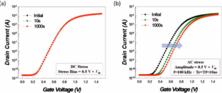
Figure 1共a兲 shows the Id-Vg transfer characteristic curves with 50 mV drain voltage under initial and after static
a兲Author to whom correspondence should be addressed. Electronic mail: [email protected].
FIG. 1. 共Color online兲 Id-Vg transfer characteristic curves of high-k/metal gate MOSFETs as function of stress time under 共a兲 dc stress and 共b兲 ac stress. The sweep was done at Vd= 0.05 V for both curves.
APPLIED PHYSICS LETTERS 98, 092112共2011兲
0003-6951/2011/98共9兲/092112/3/$30.00 98, 092112-1 © 2011 American Institute of Physics
This article is copyrighted as indicated in the article. Reuse of AIP content is subject to the terms at: http://scitation.aip.org/termsconditions. Downloaded to IP: 140.113.38.11 On: Wed, 30 Apr 2014 09:17:53
stress. Obviously, the device exhibits no degradation under the static positive gate bias of 0.5 V + Vth over a period of
1000 s. However, when dynamic stress was applied to the identical device, the Vth shifts to the positive direction and
on-current is degraded after the stress, as shown in Fig.1共b兲. In addition, the transfer curves shift has not been accompa-nied by subthreshold swing degradation, meaning that there is no creation of extra interface states. Therefore, most of the
Vth shift can be attributed to the charge trapping within the
high-k dielectric layer.
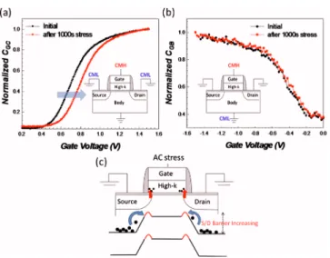
The results above are inconsistent with the general real-ization that the dynamic bias causes less degradation due to its shorter effective stress time.9 To further understand this phenomenon, the Cgb-Vg and Cgc-Vg transfer characteris-tics under initial and after dynamic stress are measured and shown in Figs.2共a兲and2共b兲, respectively. It can be observed that the Cgc-Vg curves shift in the positive direction after dynamic stress, which is consistent with the Id-Vg result in Fig.1共b兲. However, Fig. 2共b兲 shows that Cgb measured be-tween the gate and the body terminals has no significant change before and after stresses. No variation in flat band voltage suggests that in the dynamic condition, electrons cannot be really captured in throughout the overall high-k dielectric layer. Therefore, the⌬Vthin Figs.1共b兲and2共a兲can
be mainly attributed to the electrons trapped near the S/D overlap region. Figure2共c兲illustrates that the captured elec-trons raise the band energy upward and induce additional energy barriers near the S/D overlap. Both barrier heights resist the electrons supplied from the S/D, leading to the positive shift in the Cgc-Vg measurement. However, the lo-cal electrons trapped near the S/D overlap region have no influence on the charge variation during the Cgb-Vg mea-surement. Therefore, the flat band voltage in the Cgb-Vg curves has no significant change before and after stresses.
The previous proposed charge trapping model10,11 sug-gests that in the period of on-state stress, a small portion of electrons can be captured instantly in the shallow traps of the high-k dielectric, as shown in the Fig.3共a兲. Then, at off state, the built-in electronic field established by work function dif-ference between metal gate and p-substrate drives these trapped electrons to migrate toward the gate electrode by
Poole–Frenkel emission.4This same electrical field direction during on-state and off-state continuously drives these elec-tions, captured in shallow traps, toward the gate electrode. Therefore, few electrons can be captured in the deep traps of high-k dielectric above the channel region. This is also the reason why the charge trapping phenomenon cannot be ob-served under static bias stress. The constant electrical field drives the electrons to migrate toward the gate electrode con-tinuously, leading to few electrons captured in the deep traps. When we consider the S/D overlap region, the on-state bias results in the electrons still being captured in the shallow traps, as shown in Fig.3共b兲. In the off-state stress, however, due to the positive value of work function difference be-tween TiN and N+S/D, a contrary direction of electrical field exists and prompts the trapped electrons to migrate toward the N+S/D. The different electrical field directions between on and off states does not allow these electrons in the shal-low traps to have sufficient time to escape from the high-k dielectric. This significantly increases the possibility of elec-tron capture in the deep traps of high-k dielectric.
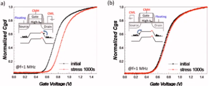
To further confirm this phenomenon, the dynamic stress condition was imposed upon an identical device, with the exception of a floating source terminal. The gate-to-drain capacitance共Cgd兲 and gate-to-source capacitance 共Cgs兲 mea-surements before and after stress are shown in Figs.4共a兲and
4共b兲, respectively. After the stress, the Cgd-Vg curves have a similar shift to those in Fig. 2共a兲 due to the energy barrier induced by trapped electrons in the drain overlap region, as shown in the inset of Fig.4共a兲. However, Fig.4共b兲shows no significant change in the Cgs-Vg curves under this stress condition. This evidence indicates that there is no additional energy barrier near the source overlap region, due to the fact that the dynamic bias cannot be applied across the overlap region between the gate and floating source terminals. This result further verifies that charge trapping in the overlap re-gion is an effect of variation in electrical field.
In summary, we observed that the Vthinstability induced
by charge trapping under dynamic stress was more serious than under static stress. C-V techniques verified that electron
FIG. 2. 共Color online兲 共a兲 Cgc-Vg and 共b兲 Cgb-Vg transfer characteristics under initial and after dynamic stress. The inset shows their respective mea-surement method.共c兲 Schematic diagram of the high-k/metal gate MOSFET and its energy-band diagram after dynamic stress.
FIG. 3. 共Color online兲 Variation in energy-band diagram cutting from 共a兲 channel region and共b兲 S/D overlap region during dynamic stress.
092112-2 Dai et al. Appl. Phys. Lett. 98, 092112共2011兲
This article is copyrighted as indicated in the article. Reuse of AIP content is subject to the terms at: http://scitation.aip.org/termsconditions. Downloaded to IP: 140.113.38.11 On: Wed, 30 Apr 2014 09:17:53
trapping under ac stress is located in the high-k dielectric near the S/D overlap region rather than throughout the over-all dielectric. This can be attributed to the influence of dif-ferent electrical field directions in the S/D overlap region during dynamic stress. These results suggest that the overlap region in high-k/metal gate stacks is the primary charge trap-ping issue in the real circuit operation.
Part of this work was performed at United Microelec-tronics Corporation. The work was supported by the National Science Council under Contract Nos. NSC99-2120-M-110-001 and NSC-97-2112-M-110-009-MY3.
1Y. Kim, G. Gebara, M. Freiler, J. Barnett, D. Riley, J. Chen, K. Torres, J. E. Lim, B. Foran, F. Shaapur, A. Agarwal, P. Lysaght, G. A. Brown, C. Young, S. Borthakur, H. J. Li, B. Nguyen, P. Zeitzoff, G. Bersuker, D. Derro, R. Bergmann, R. W. Murto, A. Hou, H. R. Huff, E. Shero, C. Pomarede, M. Givens, M. Mazanec, and C. Werkhoven, Tech. Dig. - Int. Electron Devices Meet. 2001, 455.
2C. Hobbs, H. Tseng, K. Reid, B. Taylor, L. Dip, L.Hebert, R. Garcia, R. Hegde, J. Grant, D. Gilmer, A. Franke, V. Dhandapani, M. Azrak, L. Prabhu, R. Rai, S. Bagchi, J. Conner, S. Backer, F. Dumbuya, B. Nguyen, and P. Tobin, Tech. Dig. - Int. Electron Devices Meet. 2001, 651. 3M. Casse, L. Thevenod, B. Guillaumot, L. Tosti, F. Martin, J. Mitard, O.
Weber, F. Andrieu, T. Ernst, G. Reimbold, T. Billon, M. Mouis, and F. Boulanger,IEEE Trans. Electron Devices 53, 759共2006兲.
4G. Ribes, J. Mitard, M. Denais, S. Bruyere, F. Monsieur, C. Parthasarathy, E. Vincent, and G. Ghibaudo,IEEE Trans. Device Mater. Reliab. 5, 5
共2005兲.
5S. Zafar, A. Callegari, E. Gusev, and M. V. Fischetti,J. Appl. Phys. 93, 9298共2003兲.
6G. Bersuker, J. H. Sim, C. D. Young, R. Choi, P. M. Zeitzoff, G. A. Brown, B. H. Lee, and R. W. Murto, Microelectron. Reliab. 44, 1509
共2004兲.
7A. Kerber, E. Cartier, L. Pantisano, R. Degraeve, T. Kauerauf, Y. Kim, A. Hou, G. Groeseneken, H. E. Maes, and U. Schwalke,IEEE Electron De-vice Lett. 24, 87共2003兲.
8H. R. Harris, R. Choi, J. H. Sim, C. D. Young, P. Majhi, B. H. Lee, and G. Bersuker,IEEE Electron Device Lett. 26, 839共2005兲.
9W. Abadeer and W. Ellis, IEEE Int. Reliab. Phys. Symp. Proc. 2003, 17. 10L. Pantisano, E. Cartier, A. Kerber, R. Degraeve, M. Lorenzini, M. Ros-meulen, G. Groeseneken, H. E. Maes, and IMEC, Dig. Tech. Pap. - Symp. VLSI Technol. 2002, 163.
11G. Bersuker, J. H. Sim, C. S. Park, C. D. Young, S. V. Nadkarni, R. Choi, and B. H. Lee,IEEE Trans. Device Mater. Reliab. 7, 138共2007兲.
FIG. 4. 共Color online兲 共a兲 Cgd-Vg and 共b兲 Cgs-Vg transfer characteristics under initial and after dynamic stress. The inset shows their respective mea-surement method and illustrates the energy-band diagram after dynamic stress for a device with a floating source.
092112-3 Dai et al. Appl. Phys. Lett. 98, 092112共2011兲
This article is copyrighted as indicated in the article. Reuse of AIP content is subject to the terms at: http://scitation.aip.org/termsconditions. Downloaded to IP: 140.113.38.11 On: Wed, 30 Apr 2014 09:17:53