Improved contact performance of GaN film using Si diffusion
C. F. Lin, H. C. Cheng, G. C. Chi, C. J. Bu, and M. S. Feng
Citation: Applied Physics Letters 76, 1878 (2000); doi: 10.1063/1.126198 View online: http://dx.doi.org/10.1063/1.126198
View Table of Contents: http://scitation.aip.org/content/aip/journal/apl/76/14?ver=pdfcov Published by the AIP Publishing
Articles you may be interested in
Low-resistance Ohmic contacts developed on undoped Al Ga N Ga N -based high electron mobility transistors with AlN interlayer
J. Vac. Sci. Technol. B 24, 2723 (2006); 10.1116/1.2395964
Low resistance ohmic contact to p -type GaN using Pd Ir Au multilayer scheme J. Vac. Sci. Technol. B 23, 1072 (2005); 10.1116/1.1924416
Dopant activation and ultralow resistance ohmic contacts to Si-ion-implanted GaN using pressurized rapid thermal annealing
Appl. Phys. Lett. 85, 5254 (2004); 10.1063/1.1828237
Thermally-stable low-resistance Ti/Al/Mo/Au multilayer ohmic contacts on n– GaN J. Appl. Phys. 92, 1712 (2002); 10.1063/1.1491584
Low-resistance Ti/Al/Ti/Au multilayer ohmic contact to n- GaN J. Appl. Phys. 89, 6214 (2001); 10.1063/1.1350617
This article is copyrighted as indicated in the article. Reuse of AIP content is subject to the terms at: http://scitation.aip.org/termsconditions. Downloaded to IP: 140.113.38.11 On: Thu, 01 May 2014 07:53:37
Improved contact performance of GaN film using Si diffusion
C. F. Lina) and H. C. ChengDepartment of Electronics Engineering and Institute of Electronics and Semiconductor Research Center, National Chiao Tung University, Hsinchu 30049, Taiwan, Republic of China
G. C. Chi
Department of Physics, National Central University, Chungli, Taiwan, Republic of China
C. J. Bu and M. S. Feng
Institute of Materials Science and Engineering, National Chiao Tung University, Hsinchu 30049, Taiwan, Republic of China
共Received 1 December 1999; accepted for publication 7 February 2000兲
In this letter, we investigate a metalization process for reducing the contact resistance on undoped GaN layers. The Si metal source was diffused successfully into the GaN films by using SiOx/Si/GaN/Al2O3 structures. By using a high-temperature annealing process, we diffused and activated the Si atoms into the GaN film. This caused a heavy doped n-type GaN layer to be formed near the GaN surface. Under high temperatures, such as a diffusion process at 1000 °C, the as-deposited Ni/Al/Ti contact had good ohmic properties and a low specific contact resistivity (c)
of 1.6⫻10⫺3⍀ cm2. Rapid thermal annealing the contact at 800 °C for 30 s caused the c to
decrease rapidly to 5.6⫻10⫺7⍀ cm2. The Ni/Al/Ti contact characteristics on the GaN films diffused at various temperatures are also discussed. © 2000 American Institute of Physics.
关S0003-6951共00兲02114-8兴
Gallium nitride is a direct wide-band-gap semiconduc-tor. It has attracted considerable interest for applications in blue-green, green, and ultraviolet light-emitting diodes, laser diodes, high-electron mobility transistors, and photoconduc-tive detectors. Conventional metalization gives high-contact resistance that limits the GaN device’s performances. Lin et al. achieved a low-resistance ohmic contact to n-GaN us-ing Al/Ti metalization with 900 °C rapid thermal annealus-ing
共RTA兲 for 30 s. The resulting value for the specific contact
resistivity was 8⫻10⫺6⍀ cm2.1 It has also been reported that using Si-doped2 and Si-implanted3,4 n-type GaN layers has been successful in reducing contact resistance. For ohmic contact to be enhanced in heavy Si-doping GaN films, the tunneling process is the best way to reduce specific contact resistivity. In this work, the Si-diffusion process and ohmic contact properties on GaN films are discussed. Our results show that the nonalloyed Ni/Al/Ti metal layers on Si-diffused GaN films exhibit ohmic behavior. We achieved our lowest specific contact resistivity by using the Si-diffusion and metal-alloyed process to undoped GaN films.
The undoped GaN films were grown by metal–organic chemical-vapor deposition on polished optical-grade C-face
共0001兲 sapphire substrates. The sapphire was placed on a
graphite susceptor in a horizontal-type reactor with a rf heater. Triethylgallium 共TEGa兲 and ammonia (NH3) were used as the Ga and N sources, respectively. The carrier gas was hydrogen (H2) and the growth pressure was kept at 100 mbar. The GaN buffer layer was grown at 525 °C, which was lower than the normal-grown 1025 °C temperature for the GaN epitaxial layer. Once the buffer layer was grown, the temperature was raised to 1025 °C for the GaN epitaxial layer growth.5 After the material was grown, the undoped
GaN films were prepared for the Si-diffusion experiment. The schematic diagram of the deposited Si metal films on the GaN epitaxial layers prior to the SiO2 caps is illustrated in
Fig. 1. The specimens were cleaned in BOE enchant for 5 min before evaporating the Si metal. The sandwich structure consisted of a 500-Å-thick Si metal layer deposited directly on the GaN, followed by a 1000-Å-thick SiO2cap layer. The
Si metal layers were deposited by an e-gun deposition sys-tem with the evaporation chamber below 2⫻10⫺6Torr. The SiO2 cap layer was deposited by photo-CVD. The
SiOx/Si/GaN/Al2O3 structures were used to prevent the Si
metal from out-diffusing on the GaN surface so that the Si atoms were diffused into GaN films. In this series of samples, the GaN films were diffused at varied the tempera-tures as follows: 825 °C 共sample B兲, 875 °C 共sample C兲,
a兲Electronic mail: [email protected] FIG. 1. Schematic drawing showing the structure of Si-diffused samplesthat contain diffusion metal layers and SiO
xcap layers.
APPLIED PHYSICS LETTERS VOLUME 76, NUMBER 14 3 APRIL 2000
1878
0003-6951/2000/76(14)/1878/3/$17.00 © 2000 American Institute of Physics
This article is copyrighted as indicated in the article. Reuse of AIP content is subject to the terms at: http://scitation.aip.org/termsconditions. Downloaded to IP: 140.113.38.11 On: Thu, 01 May 2014 07:53:37
935 °C 共sample D兲, and 1000 °C 共sample E兲. They were put in a nitrogen ambient furnace for 2 h and sample A was the standard GaN sample, without the diffusion process. After the thermal diffusion process, a chemical solution consisting of HF, HNO3, and CH3COOH at a ratio of 6:20:7 was used to remove the metal and cap layers. These Si-diffused GaN films were rinsed in deionized water, so that the ohmic con-tact property on the diffused GaN films could be studied in this experiment.
Through reactive ion etching共RIE兲, the mesa region of the GaN films was defined for the use of the transmission line measurement method共TLM兲. BCl3gas was used to etch
the GaN films at an etching rate of 600 Å/min with a 2m etching depth. The flow rate, the rf power, and the pressure were fixed at 5 sccm, 120 W, and 24 mTorr, respectively. The dimensions of the metal contact pads were 200m wide and 100 m long. The gaps between the two contact pads ranged from 20 to 120 m with 20 m increments. The Si-diffusion depth in the GaN films was 0.15 m at a 1000 °C annealing temperature, observed from secondary ion mass spectrometry 共SIMS兲 profiles. The Ni/Al/Ti 共300 Å/1200 Å/150 Å兲 metal pads were deposited by using the e-beam evaporator. These metal contact pads were defined on the mesa region by using a photoresist lift-off technique. The specimens were treated in a RIE system for the second time to etch the Si-diffused layer between the two contact pads. The thin Ni metal layer was used as a RIE metal mask to protect the metal layer during the RIE treatment. After the treatments, the specimens were alloyed by rapid thermal an-nealing at 800 °C for 30 s.
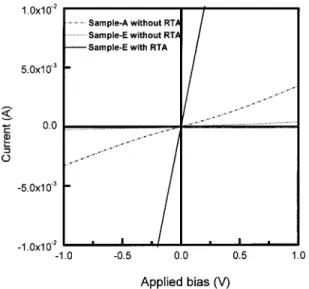
The current–voltage (I – V) characteristics of the metal contacts to the Si-diffused GaN films before and after ther-mal alloying are shown in Fig. 2. These three curves show the contact properties of sample A without RTA, sample E without RTA, and sample E with alloyed RTA, using Ni/ Al/Ti 共300 Å/1200 Å/150 Å兲 layers as the ohmic contact metals, respectively. Sample A without the alloyed RTA ex-hibited nonlinear I – V characteristics, which were probably due to the formation of a Schottky contact. Sample E without the alloyed RTA, in the linear I – V curve, showed ohmic
behavior on the Si-diffused GaN film. In this experiment with the metal contact on Si-diffused GaN films, we got ac
value of 1.6⫻10⫺3⍀ cm2, even for the nonalloyed Ni/Al/Ti ohmic contacts. This implied that the Si atoms had been diffused and activated during the high-temperature diffusion process. The heavy n-type GaN layers from the Si-diffusion treatment provided the current tunneling through the barrier height at the metal/GaN interface. During the high-temperature diffusion process, there is a probable mechanism that lets the nitrogen atoms escape from the GaN leaving vacancies6to form the donor sites for the Si atoms. The third I – V curve for sample E with the alloyed RTA exhibited a sharp linear I – V curve and lower overall contact resistance characteristics.
On the fabricated TLM patterns, the RT valves 共total
resistance兲 were measured using the four-point-probe method. The dimensions of the contact pads and the contact spacing were measured by a scanning electron microscope. The RTdata for samples D and E with the alloyed RTA were
plotted as functions of the distance for the separated contact pads, as shown in Fig. 3. The contact resistance was deter-mined from the intercepts of the least-squares linear fitting line in the resistance versus distance plot. The total contact resistance for the alloyed RTA at 800 °C was measured and the specific contact resistivities c were calculated from the TLM method. The specific contact resistivities c were duced by increasing the diffusion temperatures. The total re-sistance of samples D and E with the alloyed RTA at 800 °C varied with the contact pad spacing, as shown in Fig. 3. The specific contact resistivities c of samples D and E are
cal-culated as 1.9⫻10⫺6 and 5.6⫻10⫺7⍀ cm2according to the TLM method. The as-deposited Ni/Al/Ti contact on sample A, without RTA, had a non-ohmic property because of a lower carrier concentration of 1.8⫻1017cm⫺3 and a higher barrier of Ti metal.7However, the as-deposited Ni/Al/Ti con-tact had an ohmic property on the Si-diffused GaN film at 1000 °C 共sample E兲 and the specific contact resistivity c
was measured as 1.6⫻10⫺3⍀ cm2. The reason is the same as in past reports about the results of contact on heavy
Si-FIG. 2. Current–voltage (I – V) characteristics of the metal contact on sample A without RTA and sample E with and without alloyed RTA mea-sured from the HP-4156 system.
FIG. 3. Total contact resistance as a function of the Ni/Al/Ti metal pad spacing of samples D and E. All contacts were RTA alloyed at 800 °C for 30 s.
1879
Appl. Phys. Lett., Vol. 76, No. 14, 3 April 2000 Linet al.
This article is copyrighted as indicated in the article. Reuse of AIP content is subject to the terms at: http://scitation.aip.org/termsconditions. Downloaded to IP: 140.113.38.11 On: Thu, 01 May 2014 07:53:37
doped and Si-implanted GaN films. The Si-diffused process forms a high surface density of donors to provide the tunnel-ing process at the metal/GaN interface.
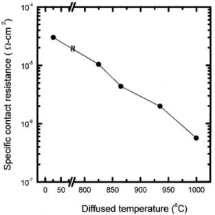
Ni/Al/Ti metal on Si-diffused GaN films was RTA al-loyed at 800 °C for 30 s in N2 ambient and the total
resis-tance RT was measured as the function of the metal pad
spacing to calculate its c value. The specific contact
resis-tivities c as functions of Si-diffused temperatures on GaN
films are shown in Fig. 4. The specific contact resistivityc
decreases with increasing Si-diffused temperatures. From ob-servation of SIMS depth profiles of Si-diffused GaN films, the number of Si atoms increased when the diffused tempera-tures were raised from 825 to 1000 °C. Large amounts of Si atoms were diffused near the surface to form the heavy Si-doped n⫹-GaN layer of sample E. This Si-diffused process caused the contact resistance to decrease, specifically thec
values observed decreased from 3.0⫻10⫺5 to 5.6
⫻10⫺7⍀ cm2. Ti is the most important metal in the Al/Ti
contact because it reduces the gallium oxide, so that the Al
can diffuse through the Ti to reach the GaN surface. The Al–Ti intermetallic phase has a lower work function1共lower than 0.07 eV兲,2 and the Al also has the same properties to help reduce contact resistivity. In addition to the lower metal work function, Si-diffused n⫹-GaN surfaces also provide the tunneling process for the electrons. These two important pa-rameters have a strong influence on the specific contact re-sistivity c of GaN epitaxial films. Our experiment has
shown another way to form heavy Si doping on the GaN surface to help reduce contact resistance.
In conclusion, Si was successfully diffused into GaN films using SiOx/Si/GaN/Al2O3 structures. SIMS analyzed the diffusion profiles of Si, and large quantities of Si atoms were diffused into the GaN surfaces to form highly doped n⫹-type GaN layers. This Si-diffused process caused the ohmic contact resistance to clearly decrease. The specific contact resistivitycvalues were reduced from 3.0⫻10⫺5to
5.6⫻10⫺7⍀ cm2for the Ni/Al/Ti metal contact, and the dif-fusion temperature increased from 825 to 1000 °C. This tech-nique to form diffused n⫹-type GaN thin layers can be used to fabricate GaN-based devices with good ohmic contact.
The National Science Council of Taiwan, R.O.C., under Contact No. NSC 89-2215-E-009-069, has supported this re-search. Technical support from the Semiconductor Research Center at the National Chiao-Tung University is also ac-knowledged.
1
M. E. Lin, Z. Ma, F. Y. Huang, Z. F. Fan, L. H. Allen, and H. Morkoc¸, Appl. Phys. Lett. 64, 1003共1994兲.
2J. D. Guo, C. I. Lin, M. S. Feng, F. M. Pan, G. C. Chi, and C. T. Lee, Appl. Phys. Lett. 68, 235共1996兲.
3L. F. Lester, J. M. Brown, J. C. Ramer, L. Zhang, S. D. Hersee, and J. C. Zolper, Appl. Phys. Lett. 69, 2737共1996兲.
4J. Burm, K. Chu, W. A. Davis, W. J. Schaff, L. F. Eastman, and T. J. Eustis, Appl. Phys. Lett. 70, 464共1997兲.
5C. F. Lin, G. C. Chi, M. S. Feng, J. D. Guo, J. S. Tsang, and J. M. Hong, Appl. Phys. Lett. 68, 3758共1996兲.
6
C. J. Sun, P. Kung, A. Saxler, H. Ohsato, E. Bigan, M. Razeghi, and D. K. Gaskill, J. Appl. Phys. 76, 236共1994兲.
7S. C. Binari, H. B. Dietrich, G. Kelner, L. B. Rowlan, K. Doverspike, and D. K. Gaskill, Electron. Lett. 30, 909共1994兲.
FIG. 4. Specific contact resistivitiescon Si-diffused GaN films with
al-loyed RTA as functions of diffusion temperatures in the N2ambient.
1880 Appl. Phys. Lett., Vol. 76, No. 14, 3 April 2000 Linet al.
This article is copyrighted as indicated in the article. Reuse of AIP content is subject to the terms at: http://scitation.aip.org/termsconditions. Downloaded to IP: 140.113.38.11 On: Thu, 01 May 2014 07:53:37