2050 IEEE PHOTONICS TECHNOLOGY LETTERS, VOL. 18, NO. 19, OCTOBER 1, 2006
Enhancement of InGaN–GaN Indium–Tin–Oxide
Flip-Chip Light-Emitting Diodes With TiO
2
–SiO
2
Multilayer Stack Omnidirectional Reflector
C. H. Lin, C. F. Lai, T. S. Ko, H. W. Huang, H. C. Kuo, Member, IEEE, Y. Y. Hung, K. M. Leung, C. C. Yu,
R. J. Tsai, C. K. Lee, T. C. Lu, and S. C. Wang, Senior Member, IEEE
Abstract—Enhancement of light extraction of GaN-based
flip-chip indium–tin–oxide light-emitting diodes (FC ITO LEDs) with an omnidirectional reflector (ODR) is presented. The ODR con-sisting of alternating layers of TiO2 and SiO2 is designed to pos-sess a complete photonic bandgap within the blue region of interest, and it is fabricated byE-beam deposition. At a driving current of 300 mA and a chip size of 1 mm2 1 mm, the light output power of the FC ITO LEDs with the ODR reaches 156 mW. This is an en-hancement of 31% when compared with the same device with an Al mirror instead. Furthermore, by examining the radiation pat-terns, the FC ITO LED with the ODR shows stronger enhancement around the vertical direction. Our work offers promising potential for enhancing output powers of commercial light-emitting devices.
Index Terms—Flip-chip (FC), GaN, indium–tin–oxide (ITO),
light-emitting diodes (LEDs), omnidirectional reflector (ODR), one-dimensional photonic crystal (1-D PhC).
I. INTRODUCTION
T
HE availability of higher brightness, higher power, and larger area of GaN-based light-emitting diodes (LEDs) has enabled their applications in outdoor displays, exterior automo-tive lightings, backlight for various handheld devices, printers, LCD TVs, and rear projection TVs [1]. To further reduce the cost and enhance the performance of these LEDs, there is always a great need to improve the internal as well as external quantum efficiency (EQE) in order to further increase their light output power. However, it is well known that LEDs are inherently in-efficient because photons generated by spontaneous emission within the device are emitted in all directions with random po-larizations. To improve the EQE and the output power of pack-aged LEDs, light emitted downward toward the substrate must be reflected upward in order to contribute to usable light output [1]–[3].Manuscript received February 7, 2006; revised July 15, 2006. This work was supported by the National Science Council NSC94-2752-E009-007-PAE, NSC94-2120-M009-007 Republic of China. The work of K. M. Leung was supported in part by the United States Army Research Office under Grant W911NF-04-1-0231.
C. H. Lin, C. F. Lai, T. S. Ko, H. W. Huang, H. C. Kuo, T. C. Lu, and S. C. Wang are with the Institute of Electro-Optical Engineering, National Chiao Tung University, Hsinchu 30050, Taiwan, R.O.C. (e-mail: [email protected]. edu.tw).
Y. Y. Hung, C. C. Yu, and R. J. Tsai are with the HighLink Technology Cor-poration, ChuNan 350, Taiwan, R.O.C.
K. M. Leung is with the Department of Computer and Information Science, Polytechnic University, Brooklyn, NY 11201 USA.
C. K. Lee is with the Institute of Electro-Optic Engineering, National Sun Yat-Sen University, Kaohsiung 80424, Taiwan, R.O.C.
Digital Object Identifier 10.1109/LPT.2006.883330
Metallic mirrors have been used for this purpose [4]. Al-though they reflect light at arbitrary angles and polarizations, they are somewhat lossy in the visible [6] and have mechanical problems at the interface with semiconductor. In particular, a re-cent work indicated that absorption by metallic mirrors becomes more severe as the thickness of the device is reduced [7]. As a result, distributed Bragg reflectors (DBRs) [5] have been used. They have many advantages, such as low optical loss, high re-flectance, and high mechanical robustness, compared with their metallic counterpart [8]. However, only light of a given polariza-tion impinging near the normal direcpolariza-tion to the DBR structure can be effectively reflected.
Total reflection of light with an arbitrary polarization at an ar-bitrary incidence angle onto a periodic structure can be realized with the existence of a complete photonic bandgap (CPBG) at the wavelengths of interest. A one-dimensional (1-D) periodic dielectric structure possessing this characteristic is known as an omnidirectional 1-D photonic crystal (PhC). Since there is no allowed photon propagation states for wavelengths within the CPBG, an omnidirectional reflector (ODR) made from such 1-D PhC can totally reflect the light with wavelength in the CPBG at any incidence angle and polarization. Therefore, compared with a DBR mirror, a substantially higher reflectance can be achieved. In our previous work, we have demonstrated an 80% enhancement in the extracted light intensity for a GaN-based LED incorporated with an ODR composed of alternate layers of TiO and SiO [2].
Light that propagates upward above the active layer can still be scattered and absorbed by the electrode wires and bonding pads at the top of our device, and thus reducing the external ex-traction efficiency. In this work, this problem is dealt with by in-tegrating flip-chip (FC) technology into the LED chip processes to eliminate bonding pads and wires at the top of the device. A layer of electrically conductive and optically transparent in-dium–tin–oxide (ITO) is introduced to help spread the current and provide connection to the p-contacts from the bottom. In ad-dition, an ODR is deposited at the bottom of the device to reflect light upward, as well as around the sides to reduce the amount of light that leaks out sideways. Another difference between the ODR here and in our previous work is that the ODR here is lo-cated between air and the ITO layer rather than sapphire.
In this letter, we report enhanced light extraction of nitride-based FC ITO LEDs with an ODR. The ODR, designed to pos-sess a CPBG within the blue regime, is located between the ITO layer and air. It is made from TiO –SiO by -beam deposition. At a driving current of 300 mA with a chip size of 1 mm 1 mm, the light output power of our FC ITO LED with the ODR reaches
LIN et al.: ENHANCEMENT OF InGaN–GaN ITO FC LEDs WITH TiO –SiO MULTILAYER STACK ODR 2051
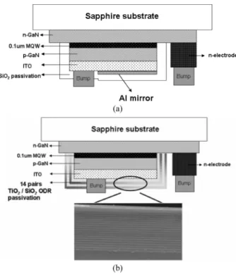
Fig. 1. Schematic diagram of the GaN-based FC ITO LEDs (a) containing an Al mirror with SiO passivation, and (b) containing the TiO –SiO ODR pas-sivation fabricated at the bottom. The inset shows the SEM picture of the 1-D PC.
156 mW. This gives an enhancement of 31% when compared with the same device with an Al mirror instead. Improvement in the light output power of the device is attributed to the better reflectivity and much lower absorption loss of the ODR.
II. EXPERIMENTS
Our GaN-based LED samples were grown by metal–or-ganic chemical vapor deposition with a rotating-disk reactor (Emcore) on a -axis sapphire (0001) substrate at the growth pressure of 200 mbar. Fig. 1 is a schematic diagram of the FC ITO LED with (a) Al mirror and (b) ODR with 14 pairs of TiO and SiO layers. The actual thickness of the sapphire substrate is much larger than that of the epitaxial layers. The LED structure is similar to [2]. The FC ITO LEDs with Al mirror were fabricated using standard process with a mesa area of 1 mm 1 mm, very similar to [3]. We partially inductively coupled plasma-reactive ion etcher etched the surfaces of the LED samples using –Ar as the etching gas until the n-type GaN layers were exposed. A 300-nm-thick ITO layer and a 300-nm-thick Al mirror were subsequently evaporated onto the sample surface. The ITO layer had a high electrical conduc-tivity and a high transparency ( 95% at 460 nm). Ti–Al–Ni–Au contacts were subsequently deposited onto the exposed n-type GaN layers to serve as the n-type electrodes. SiO layers were then deposited over all wafers by plasma-enhanced chemical vapor deposition. Photolithography and HF solution etching were subsequently performed to define the P/N pad pattern for bump electroplating. Step coverage of the SiO films was well controlled to cover the entire chips, as shown in Fig. 1(a). Au Sn solder was used for electrical and mechanical in-terconnection because of its very high reliability due to its good mechanical properties, good thermal conductivity, and low growth of intermetallic phase. Au –Sn (1600/400 nm)
Fig. 2. Photonic band diagram of a 1-D PC composed of TiO and SiO mul-tilayers. Refractive indexes and layer thickness are assumed to ben = 2:52, d = 56 nm for TiO and n = 1:48, d = 77 nm for SiO . The gray and white regions distinguish between the allowed and forbidden photon states, re-spectively. The lines in the diagonal directions identify the edges of the light cone. The grayish white region of the CPBG represents an omnidirectional re-flection region.
layers were then evaporated onto the samples while P/N bumps were defined by the liftoff process. During the bonding process, chips were picked, orientated, and flipped by a die bonder system. The FC ITO LED was soldered onto an AlN submount. For comparison reasons, FC ITO LEDs with Al mirror and FC ITO LEDs with TiO –SiO ODR were fabricated from exactly the same epitaxial wafer with the same chip size, and then chosen for the same chip brightness and wavelength on the fabricated wafer.
Fig. 1(b) shows the schematic structure of FC ITO LEDs with ODR. After front end processing, an ODR with 14 pairs of TiO –SiO (see inset in Fig. 1(b) for a scanning electron mi-croscope (SEM) picture) was evaporated onto FC ITO LEDs by an -beam evaporator at 150 C, and at an oxygen partial pres-sure of Torr with Ar and O as the ion source inlet gases. The film deposition rates of TiO and SiO were 0.4 and 0.8 nm/s, respectively. It should be noted that the ODR is well controlled to cover the entire chip surface to serve as a good pas-sivation layer as well and to reflect also light from the side walls of the device.
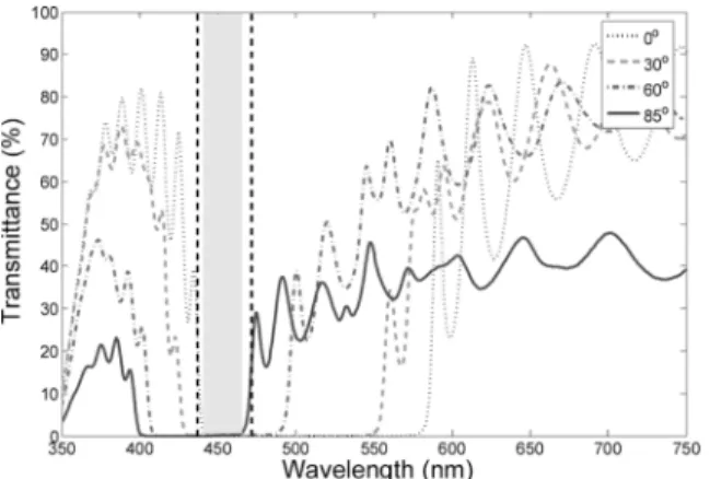
The band structures of a 1-D PhC composed of TiO and SiO with reflective indexes of 2.52 and 1.48, respectively, and var-ious thicknesses were calculated by the modal transmission-line method [9], as shown in Fig. 2. We found the most optimal CPBG at frequencies between 0.282 and 0.304 (e.g., the grayish white region), where is the speed of light and is the lattice constant for thicknesses of 0.421 and 0.579 , re-spectively, for the TiO and SiO layers. We chose the lattice constant nm to give a CPBG centered at 455 nm. Thus, we found that our ODR has a CPBG between 437 and 472 nm if the TiO and SiO layers have a thickness of 56 and 77 nm, respectively. Fig. 3 shows the measured transmit-tance of our ODR with an ITO cover and an air ambient. The figure shows the transmittance at incidence angles of 0 , 30 , 60 , and 85 for unpolarized light as a function of the wave-length. We observed that rather high reflectance ( 99.5%) can be achieved from 441 to 465 nm, and up to an incidence angle of 85 (e.g., the grayish white region). This wavelength region falls in the CPBG, as shown in the dashed line region, and this is expected from the photonic band diagram Fig. 2. As the number
2052 IEEE PHOTONICS TECHNOLOGY LETTERS, VOL. 18, NO. 19, OCTOBER 1, 2006
Fig. 3. Measurement transmittance results of the four transmittance curves with different incidence angles (e.g., 0 , 30 , 60 , 85 ) for unpolarized light versus wavelength.
Fig. 4. ELL–I characteristics of the FC ITO LEDs with TiO –SiO ODR, FC ITO LEDs with Al mirror, and conventional face up ITO LEDs, respectively. The inset shows the room-temperature EL spectra.
of TiO –SiO pair increases, this high reflectivity region is ex-pected to approach the result given by the CPBG. We note that the ambience of our ODR is 300 nm of ITO, which has a refrac-tive index of 1.9, smaller than that of the GaN [6].
III. RESULTS ANDDISCUSSION
We performed electroluminescence (EL) measurements by injecting a continuous current into our LEDs at room temper-ature. The light output was detected by a calibrated an inte-grating sphere with Si photodiode on the package device. It was found that the – curves were almost identical for these two devices. The 300-mA forward voltages were both around 3.34 V for the FC ITO LED with TiO –SiO ODR and FC ITO LED with Al mirror. The slightly higher forward voltage of FC ITO LEDs with TiO –SiO ODR than those with Al mirror can be attributed to additional thermal processes during the ODR depo-sition. We believe that ITO/SPS layer interfacial mixing could result in a higher specific contact resistance and hence could raise the LED operation voltage.
We incorporated TiO –SiO ODR onto the bottom of our GaN-based FC ITO LEDs with a reflectance peak at 455 nm and a full-width at half-maximum of about 20 nm. The inten-sity–current ( – ) characteristics of the three different types of LEDs were shown in Fig. 4. We clearly observed that the output powers of the FC ITO LEDs with TiO –SiO ODR were larger than those of the FC ITO LEDs with Al mirror. At an in-jection current of 300 mA, it is found that the MQW emission
peaks of those three devices are located at about 455 nm, and the light output powers of the FC ITO LEDs with TiO –SiO ODR, FC ITO LEDs with Al mirror, and conventional face up ITO LEDs are about 156, 119, and 68 mW, respectively. In other words, both FC ITO LED with our designed ODR and FC ITO LED with Al mirror show output power enhancement by 129% and 75%, respectively, when compared to the conventional face up ITO LED. At an injection current of 300 mA, the EQE of FC ITO LED with TiO –SiO ODR and FC ITO LED with Al mirror are estimated to be approximately 19.1% and 14.8%, re-spectively. The inset of Fig. 4 shows the typical room-tempera-ture EL spectra of FC ITO LEDs with TiO –SiO ODR and FC ITO LEDs with Al mirror at a driving current of 300 mA. The EL intensity of the FC ITO LEDs with TiO –SiO ODR was larger than that of the FC ITO LEDs with Al mirror.
IV. CONCLUSION
GaN-based FC ITO LEDs with an ODR was designed and fabricated. Our ODR consisting of TiO and SiO was de-signed to possess a CPBG within the blue region of interest. At a driving current of 300 mA and a chip size of 1 mm 1 mm, the light output power of FC ITO LEDs with the ODR reaches 156 mW. This gives an enhancement of 31% when compared with the same device with an Al mirror instead of an ODR. Furthermore, stronger enhancement around the vertical direc-tion and wider view angle as shown in the radiadirec-tion pattern for the FC ITO LEDs with TiO –SiO ODR can be attributed to the higher reflectance of our ODR when compared to that of an Al mirror. Our work offers promising potential for enhancing output powers of commercial light-emitting devices.
ACKNOWLEDGMENT
The authors would like to thank Dr. C. Kuo of LuxNet Corpo-ration, and Prof. S. Y. Lin of Rensselaer Polytechnic Institute, for useful discussion and technical support.
REFERENCES
[1] S. Nakamura, T. Mukai, and M. Senoh, “Candela-class high bright-ness InGaN/AlGaN double-heterostructure blue light-emitting diodes,” Appl. Phys. Lett., vol. 64, pp. 1687–1689, 1994.
[2] C. H. Lin, J. Y. Tsai, C. C. Kao, H. C. Kuo, C. C. Yu, J. R. Lo, and K. M. Leung, “Enhanced light output in InGaN-based light-emitting diodes with omnidirectional one-dimensional photonic crystals,” Jpn. J. Appl. Phys., vol. 45, p. 1591, 2006.
[3] S. J. Chang, C. S. Chang, Y. K. Su, C. T. Lee, W. S. Chen, C. F. Shen, Y. P. Hsu, S. C. Shei, and H. M. Lo, “Nitride-based flip-chip ITO LEDs,” IEEE Trans. Adv. Packag., vol. 28, no. 2, pp. 273–277, May 2005. [4] J. K. Kim, T. Gessmann, H. Luo, and E. F. Schubert, “GaInN
light-emitting diodes with RuO /SiO /Ag omni-directional reflector,” Appl. Phys. Lett., vol. 84, pp. 4508–4510, 2004.
[5] Y. S. Zhao, D. L. Hibbard, H. P. Lee, K. Ma, W. So, and H. Liu, “Efficiency enhancement of InGaN/GaN light-emitting diodes with a back-surface distributed Bragg reflector,” J. Electron. Mater., vol. 32, p. 1523, 2003.
[6] Y. Fink, J. N. Winn, S. Fan, C. Chen, J. Michel, J. D. Joannopoulos, and E. L. Thomas, “A dielectric omnidirectional reflector,” Science, vol. 282, pp. 1679–1682, 1998.
[7] A. David, T. Fujii, B. Moran, S. Nakamura, S. P. DenBaars, C. Weis-bush, and H. Benisty, “Photonic crystal laser lift-off GaN light-emitting diodes,” Appl. Phys. Lett., vol. 88, p. 133514, 2006.
[8] J.-Q. Xi, M. Ojha, J. L. Plawsky, W. N. Gill, J. K. Kim, and E. F. Schubert, “Internal high-reflectivity omni-directional reflectors,” Appl. Phys. Lett., vol. 87, p. 031111, 2005.
[9] C. H. Lin, K. M. Leung, and T. Tamir, “Modal transmission-line theory of three-dimensional periodic structures with arbitrary lattice configu-rations,” J. Opt. Soc. Amer. A, vol. 19, pp. 2005–2017, 2002.