Bipolar resistive switching characteristics of Gd2O3 thin film structure
K. M. Changa,b, W. H. Tzenga, K. C. Liuc, Y. C. Chanc, and C. C. Kuoc
a
Department of Electronics Engineering & Institute of Electronics, National Chiao Tung University, HsinChu, No. 1001, University Rd., 30010, Taiwan, R.O.C.
b
Department of Electronic Engineering, I-Shou University, No. 1, Sec. 1, Syuecheng Rd., Kaohsiung, 840, Taiwan, R.O.C.
c
Institute of Electro-Optical Engineering, Chang Gung University, Tao-Yuan, 33302, Taiwan, R.O.C.
The resistive switching (RS) behavior of the Ti/Gd2O3/Pt capacitor
structure is fabricated and discussed in this paper. The switching characteristics operated under positive bias exhibits stable switching properties with a condensed voltage and resistance values dispersion, while the switching characteristics becomes unstable and large fluctuation on switching parameters under the negative bias operation. We suggest that the anode electrode plays an important role to the switching characteristics, and might be the causes of the asymmetry of the I-V curves between positive and negative operation. Constant voltage stress measurement is also tested to reveal the switching mechanism of the Gd2O3 film, and
the switching mechanism is mainly based on the applied voltage and thermal Joule heat.
Introduction
Resistive random access memory (RRAM) are practically one of the interesting subjects in the field for nonvolatile memory applications because of its great affinity with the complementary metal-oxide-semiconductor (CMOS) technology, simple structure, high density, and low power consumption (1-3). Depending on the requirement of the applied bias polarity, resistive switching can be divided into “bipolar” or “unipolar” operation. The unipolar switching has the advantages of simpler circuits for memory arary application. Many candidate materials have been reported to demonstrate the switching characteristics including transition metal oxides (TMOs): HfO2, NiO, TiO2, and Cu2O
(4-7), perovskite oxide: PCMO, and LCMO (8,9) and chagenide materials. Several switching models have been proposed to explain the switching characteristics. However, some of them contradicted between each other. The resistive switching based on rare-earth oxide, such as CeO2 (10) and Gd2O3 (11) have been revealed the reversible
switchinthe characteristics. The rare-earth oxide material has been applied on the microelectronics, magnetic recording media, new superconducting components, and optoelectronic technologies for many years, however, the use for the application as RRAM device is less being discussed. Because the unipolar RS operation was reported to exhibit highly material dependence, including oxide film and electrodes, therefore, a deep investigation on the resistive switching of the Gd2O3 is essential to seek a universal
nature on various oxide materials.
In this study, the resistive memory cells employing the Gd2O3 film as the resistance
change material is fabricated and discussed here. The RS behavior, endurance, voltage dispersion, resistance values, and the polarity dependence on the unipolar operation, was
discused. We observed the electrical characteristics of Ti/Gd2O3/Pt device are dependent
to the operation polarity. This reveals that the electrodes are a critical issue to rare-earth oxide Gd2O3 film under unipolar switching.
Experiments
The Pt metal as a bottom electrode was deposited on Ti/SiO2/Si wafer by e-beam
evaporation. Then, the Gd2O3 films with a thickness of 25 nm were deposited by pulsed
layer deposition (PLD) at RT by using a metal Gd target with oxygen pressure of 0.01 Pa during deposition. PLD process can provide the advantages of transfering the complex target materials at the same time in one process. After stacking Gd2O3 thin films on the
bottom electrodes, the metal Ti used as top electrode was deposited by e-beam evaporation. The thicikness of metal is about 50 nm. Shadow mask with a diameter of 200 um was used to define contact pad for measurement. The electrical characteristics were performed on Agilent 4156C semiconductor parameter analyzer (SPA) at RT. Current flow from top to bottom electrode was defined as positive sweep.
Results and Discussion
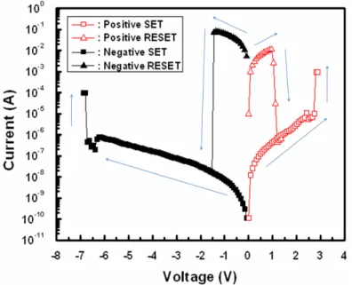
Fig. 1 shows the typical unipolar I-V curves operated under positive and negative bias. The Ti/Gd2O3/Pt resistive switching memory exhibits the nonpolar switching
characteristics which can be both operated under positive and negative bias, respectively. Before operation, the electroforming process is necessary to trigger the resistive properties. Under the applied bias, a voltage sweeps from 0 V to certain positive voltage value with a compliance current of 1 mA. The forming voltage is about 3.5 V for our Ti/Gd2O3/Pt structure. After forming process, a low resistance state (LRS) can be
obtained. When sweeping voltage value from zero to a certain positive bias next operation, a reversible switching by an abrupt drop on the current value occurred at certain voltage value, then the state was switched back to high resistance state (HRS). We defined the voltage value as Vset and Vreset where the certain voltage values trigger the
HRS to LRS and LRS to HRS switching. The reversible switching can also be performed by negative bias, as shown in Fig. 1. After forming process, the state can be switched to another HRS by applied the negative bias. The asymmetric I-V curves under the two polarity operation were clearly observed, and can be attributed to the asymmetry of our MIM structure. Since the metal Ti and Pt is respectively used as top and bottom electrode, which may cause the distinction.
! !
Figure 1. Typical nonpolar I-V characteristics of the Ti/Gd2O3/Pt capacitor structure. The
arrows indicate the applied voltage sweeping direction.
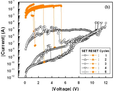
Then, the repetitive resistive switching is tested here. As it can be seen from Fig. 2(a) and 2(b), the unipolar resistive switching I-V curves of the Ti/Gd2O3/Pt memory
cells in 5 cycles could both be obtained repetitively by applying the positive or negative bias to the device. As shown in Fig. 2(a), the positive operation Gd2O3 film at a 1 mA
compliance current exhibit a high to low resistance ratio of about 1 order of magnitude. And the Vset and Vreset values are about 2-3 V and 1 V, respectively. However, the Vset
and Vreset values are distinguishable. As for the negative bias operation, the Vset values
at negative side operation of about |-11| V are much higher than that of positive side (2.5 V), while the Vreset exhibits no distinct dependence on the polarity. To evaluate the
memory performance of Ti/Gd2O3/Pt structure, we investigated measurements of the
Figure 2. The I-V curves of the Ti/Gd2O3/Pt memory cells in continuous 5 switching
cycles under (a) positive, and (b) negative bias operation.
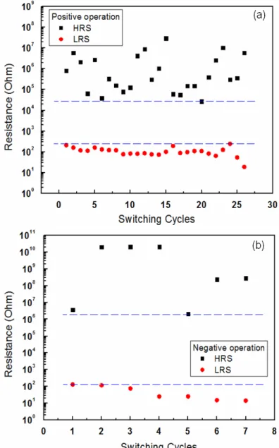
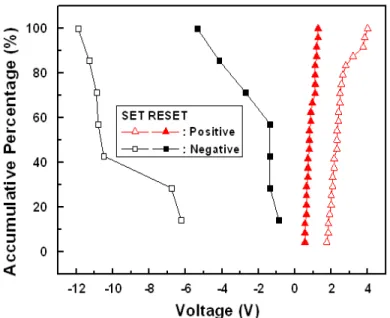
Fig 3(a) and 3(b) shows the resistance values versus switching cycles by the positive and negative bias operation, respectively. The resistance values read at 0.3 V in each dc sweep. During the repetitive switching cycles, the positive operation exhibits a high to low resistance ratio of about 1 order of magnitude during the consequent switching, while a resistance ratio of about 4 orders of magnitude was observed on the negative bias samples. However, a large dispersion on resistance values is clearly observed. Fig. 4 compares the accumulative percentage on operation voltage of the positive and negative operated devices, respectively. For the negative bias operated sample, a wide distribution on voltage values in the range of -6.2 ~ -12 V and -0.9 ~ -5.7 V for Vset and Vreset is
obtained. On the contrary, the samples operated under positive bias exhibit the stable and reliable switching characteristics, and the operation voltage values ranges from 1.2 to 2.2 V for Vset and from 0.3 to 0.9 V for Vreset values. From the collected data shown above,
distinct switching characteristics on the two operation polarity are obviously observed. We suggest that the different switching properties between positive and negative operation may be owing to the asymmetric Ti/Gd2O3/Pt stacked structure.
Taking the reported literature into consideration, we may refer that the switching mechanism is based on the formation and rupture of the conducting filamentary paths inside the Gd2O3 thin film. For the unipolar operation, the anode has been reported to be
an important factor to influence the switching characteristics. When the device is operated under positive bias, the Ti is as anode electrode. The reactive metal Ti can easily
be achieved when Pt electrode was as anode electrode (negative operation), thus causing the switching properties short-lived and unreliable.
Figure 3. Endurance test of the Ti/Gd2O3/Pt capacitor structures under (a) positive bias,
Figure 4. Comparison of the Vset and Vreset distribution of the Ti/Gd2O3/Pt memory cells
under both positive bias operation (up-triangle) and negative bias operation (square). To reveal more information about the switching mechanism, the constant voltage stress (CVS) test is also performed here. Fig 5(a) shows the time to resistive switching under the constant negative bias of -11 V. As we can see from this figure, the current values decreased step by step at the time slot of 5 and 23 s, however, a sudden increase to high current level occurred at the time slot of 40 s (indicated by arrows). It is well known that the integrity and quality of dielectric film would be gradually degraded under the voltage stress, and the percolation path is generated and breakdown (BD) takes place (11,12). However, we can observe that the phenomenon of the sudden drop on current values occurred prior to totally breakdown, which means another mechanism is triggered during the breakdown measurement. We suggest that the reversible switching characteristics correspond to the thermal destruction of the filamentary paths. Under the high constant voltage stress, the thermal Joule heat gradually accumulates inside the conducting filaments and has been simulated to be about 700-900 K (13,14). So with the increase in the measurement time, the accumulative Joule heat became higher, and the conducting filamentary paths destructed sequentially. Therefore, a two step on the current drop is observed. This result is similar to our dc sweep by voltage ramping measurement shown in Fig 2(a) and 2(b). Fig. 5(b) shows the time to resistive switching under different negative CVS of -0.5, -1.0, -1.5 and -3.2 V. As is evident from this figure, the low voltage stress can not trigger the reversible resistive switching over a period of time. However, once the applied voltage is increased to -3.2 V, the LRS can be switched back
Figure 5. (a) Current value evolution with time during CVS test. The arrows indicate the sudden change on current value. (b) Current value evolution with time during CVS test under different applied voltage.
Conclusion
To sum up, the resistance switching properties of Ti/Gd2O3/Pt device is fabricated
and discussed here. The switching characteristics operated under positive and negative exhibit quite different phenomenon. Under positive bias operation, the switching can be operated repeatedly for near 30 switching cycles with low voltage and resistance dispersion, while becomes unstable when operated under negative bias and only 7 cycles could be performed. The stress test results confirm that the resistive switching mechanism is attributed to formation and rupture of conducting paths based on thermal Joule heat. Asymmetry on the device structure may be main reason on the distinct behaviors. This work reveals the importance of anode material, and switching properties of Gd2O3 film are dependent on electrode material under unipolar operation.
Acknowledgments
This work was supported by J. P. Lin in Nanya Technology Corporation and by M. J. Tsai, P. S. Chen and H. Y. Lee in the Electronics and Optoelectronics Research Laboratory of Industrial Technology Research Institute and by the National Sciences Council (NSC 97_2221_E_182005).
References
1. S. Q. Liu and N. J. Wu, Appl. Phys. Lett., 76, 2749 (2000). 2. R. Waser and M. Aono, Nat. Mater., 6, 833 (2007).
3. A. Sawa, T. Fujii, M. Kawasaki, and Y. Tokura, Appl. Phys. Lett., 85, 4073 (2004).
4. K. Tsunoda, K. Kinoshita, H. Noshiro, Y. Yamazaki, T. Iizuka, Y. Ito, A. Takahashi, A. Okano, Y. Sato, T. Fukano, M. Aoki, and Y. Sugiyama, IEDM,
Tech. Dig., 2007, p. 767.
5. A. Chen, S. Haddad, Y. C. Wu, Z. Lan, T. N. Fang, and S. Kaza, Appl. Phys. Lett.,
91, 123517 (2007).
6. B. J. Choi, S. Choi, K. M. Kim, Y. C. Shin, C. S. Hwang, S. Y. Hwang, S. Cho, S. Park, S. K. Hong, Appl. Phys. Lett., 89, 012906 (2006).
7. K. M. Chang, W. H. Tzeng, K. C. Liu, and W. R. Lai, ECS Trans., 28, 119 (2010). 8. X. Chen, N. J. Wu, J. Strozier, and A. Ignatiev, Appl. Phys. Lett., 87, 223506
(2005).
9. R. Dong, W. F. Xiang, D. S. Lee, S. J. Oh, D. J. Seong, S. H. Heo, H. J. Choi, M. J. Kwon, M. Chang, M. Jo, M. Hasan, and H. Hwang, Appl. Phys. Lett., 90, 182118 (2007).
10. X. Sun, B. Sun, L. Liu, N. Xu, X. Liu, and R. Han, IEEE Electron Device Lett.,
30, 334 (2009).
11. X. Cao, X. Li, X. Gao, W. Yu, X. Liu, Y. Zhang, L. Chen, and X. Cheng, J. Appl.
Phys., 106, 073723 (2009).
12. G. Ribes, J. Mitard, M. Kenais, S. Bruyere, F. Monsieur, C. Parthasarathy, E. Vincent, and G. Ghibaudo, IEEE Trans. Dev. Mater. Reliab., 5, 5(2005).
13. E. Miranda, and J. Sune, Mic. Reliab., 44, 1 (2004).
14. D. C. Kim, S. Seo, S. E. Ahn, D. S. Suh, M. J. Lee, B. H. Park, I. K. Yoo, I. G. Baek, H. J. Kim, E. K. Yim, J. E. Lee, S. O. Park, H. S. Kim, U. Chung, J. T. Moon, and B. I. Ryu, Appl. Phys. Lett., 88, 202102 (2006).