Thin Solid Films 270 ( 1995) 607-611 ELSEVIER
Chemical mechanical polishing of PSG and BPSG dielectric films: the
effect of phosphorus and boron concentration
Chi-Wen Liu, Bau-Tong Dai ‘, Ching-Fa Yeh
Department of Electronics Engineering and Institute of Electronics, National Chiao Tung University, 1001 Ta Hsueh Road, Hsinchu, Taiwan
Abstract
Chemical-mechanical polishing of blanket and patterned oxide films doped with phosphorus and boron has been studied. FIIR was used to characterize the film microstructure. Experimental results show that an increase of phosphorus level promoted the polish rate of PSG film. We also found that increasing the boron content enhanced the polish rate of BPSG films although phosphorus contents is decreased. This implies that boron is more effective than phosphorus in enhancing the polishing rate of BPSG films. However, the hardness of these doped films is slightly affected by doping level. Excellent planarity achieved by CMP is demonstrated for patterned wafers. Here, we also identify inversion patterns for the composite dielectric formed by a thin hard film on the top of a thick soft film. Such inversion phenomenon can be used for monitoring CMP process as a means of end point detection.
Keywords: Dielectrics; Boron; Phosphorus; Planarization
1. Introduction
Phosphosilicate glasses (PSG) and borophosphosilicate glasses (BPSG) have been widely used in the microelectron- ics industry in the fabrication of bipolar and metal-oxide- semiconductor (MOS) devices as interlevel and intermetal dielectric films for multilevel interconnections [ 141. PSG films are used for passivation and reflow planarization of device surfaces [ 31, while BPSG films reduce reflow tem- perature because boron plays a principle role in the lowering of glass viscosity [ 1,2,4]. Furthermore, phosphorus acts to provide trapping sites for alkali metals and thus minimizes impurity penetration into sensitive derivatives [ 41.
However, when working with dimensions below 0.35 pm or with three or more levels of metals, there are several lim- itations to the use of reflow PSG and BPSG. First, the limited depth of focus of high numerical aperture lenses used in the latest generation wafer stepper for patterning smaller dimen- sion requires a flatter surface [ 5,6]. Even with higher doping levels of boron and phosphorus in the doped film, doped films still fail to provide adequate contours in the dielectric, espe- cially in the smaller line dimension [ 71.
Second, boron and phosphorus incorporated in the glass tend to react with water in the ambient air. This absorption
’ National Nano Device Laboratory.
0040-6090/95/$09.50 0 1995 Elsevier Science S.A. All rights reserved SSDIOO40-6090(95)07088-5
process is concentration dependent for both dopants. The use of higher dopant concentration to increase surface smoothing causes doped films to be a major contributor to metal line corrosion and increase the defect density to an unacceptable level in the subsequent patterned-metal layer, probably due to evolved phosphoric acid and boric acid microcrystal on the surface of dielectric [ 1,7].
Finally, PSG and BPSG require high reflow temperature of over 1000 “C and 750 “C, respectively, to create a smooth surface. This will cause unintentional dopant diffusion [4] and agglomeration of titanium silicide [7]. To overcome these problems, a Chemical-Mechanical Polishing (CMP) process [ 5-71 has been developed. In this technique, a wafer is rotated against a polish pad in the presence of slurry at a temperature slightly higher than room temperature. With adequate pad conditions, CMP has the ability to obtain a more planar surface and a significant reduction of thermal budget.
In order to use doped silica films in the semiconductor industry and to avoid their disadvantages, CMP was used to polish these films. In this paper we first investigate the change in removal rate and hardness of PSG and BPSG as a function of boron and phosphorus content. mR was used to charac- terize the film microstructure. We also reported characteri- zation of planarizing results for patterned wafer with dielectric formed by uniform and multilayered film,
2. Experimental details 2.2. Polisher setup
2.1. Sample preparatiorl CMP was carried out on a Westech Mode1 372M wafer
polisher using a IC lOOO/Suba IV pad. During the polish The USC (undoped silicate glass) and PSG films were
deposited on 150 mm P-type ( 100) silicon wafer using a Novellus plasma-enhanced chemical vapor deposition (PECVD) reactor with phosphine as a phosphorus dopant source. The flows of PH, were varied in different production runs to achieve variation in the phosphorus contents. The BPSG films were prepared in Watkins-Johnson 999 system. The wafers were held at 400 “C in a flowing gas mixture of 02, SiH,, BZHC, and PH3. PH,/B,H, gas flow ratio was varied in order to change boron and phosphorus contents in the films. After deposition, the films were annealed in N, at 900 “C for 15-20 min (THEMOCO).
experiment, the wafer was mounted on a template assembly for a single 6” diameter wafer. Pressure at the wafer-slurry- pad interface is controlled via an overhead mechanism which allows pressure in 48.3 kPa (7 psi) to be applied to the wafer holder. Both the carrier and table (with the IC lOOO/Sub IV pad fixed to the table) were rotated independently, the table at 20 rpm, the carrier at 42 rpm, respectively. The polish slurry (SC- 1 slurry available from Rippey Corporation) was a suspension of fumed silica dispersed in aqueous potassium hydroxide. The pad conditioning with Rotating Pad Condi- tioner II was performed between each wafer to clean the pad of old slurry and to lift the pad fibers for further processing. A LAMBDA 3B calorimetric system (Perkin-Elmer) was
utilized in this work to analyze both the boron and phosphorus contents, as shown in Table 1. Fourier Transform Infrared (FTIR) measurement was used to characterize the film microstructure in the wave number range from 1600 to 400 cm-’ using a Biorad QS300 FTIR spectrometer. Nanoinden- tation experiments on these PECVD films were performed using a commercially available ultra-low-load indentation system, the NANOTEST 500 from Micro Materials, Inc. Berkovich indenter was used. All tests were performed at a nominal constant loading rate of 1.18 mN s- ’ of the maxi- mum set displacement (300 nm). The load versus displace- ment curve was recorded, from which the hardness can be calculated using standard formula [ 81.
The thickness of the dielectric films was measured using Nanometrics 2100XP from 10 mm away from the edge toward wafer center, and was averaged over nine different locations on the wafer to determine the polishing rate. In order to eliminate polishing rate variation from run-to-run, a steam- grown silicon dioxide film was included in each polish run, and the polishing rate ratio is normalized to its polishing rate. The step height of a feature was determined by profilometer (Dektek 3030) scan.
3. Results and discussion
3. I. Characterization of doped$lms In preparing patterned samples, we started by patterning
metal interconnect wires on wafer, then deposited thin USG (0.1 pm), thick BPSG ( 1 p,m) and SRO (silicon rich oxide, 0.1 pm) as a polish stop layer, the polish rate ratio for BPSG to SRO is about 3: 1. Samples without a hard layer on top also were prepared for comparison.
Table 1
Summary of process conditions and contents for USG, PSG and BPSG films
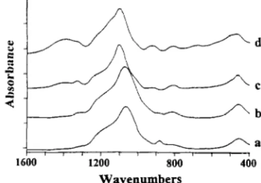
Fig. 1 clearly shows the infrared absorption spectra for PSG and BPSG films. In the PSG film, bands with 1330, 1070,8 10 and 450 cm- ’ were observed. These infrared spec- tra of the PSG film are similar to the previous works [ 1,3]. It is also observed that absorption due to the P=O stretching at 1330 cm- ’ increased as a result of a rise in the phosphorus concentration in the PSG film (a and b in Fig. 1). These findings were consistent with the previous report on PSG [31.
Sample System Gas used Boron wt% Phosphorus wt%
USG Novellus SiH,, O2 _ _
PSGI Novellus SiH,. 0,. _ 3.3
N,O, PH,
PSG2 Novellus SiH,, O,, _ 5.6
N20, PH, PBSGl WJ999 SiH,. O,, PH,, 1.4 5.8 BzHfi BPSG2 WJ999 SiH,, Oz. 2.8 4.6 PHs.BzH, BPSG3 WJ999 SiH,, O,, PH,, 4.0 4.6 J&He BPSG4 WJ999 SiH,, 02, PH,, 4.9 3.8 B>H,
For BPSG films, there is an overlap between the B-G and P=O absorption bands, hence, near the B-O peak at 1394
16UU
Note: USG is undoped silicate glass.
Fig. I. Infrared absorption spectra for PSG and BPSG films. The samples were (a) PSGl, 3.3 wt%P. (b) PSG2, 5.6wt%P. (c) BPSGl, 1.4wt%B. 5.8wt%P, and (d) BPSG4,4,9wt%B, 3.8wt%P.
1200 800
C.-W. Lilt et al. /Thin S&d Films 2 70 (I 99s) 60741 I 609
cm-‘, one can find the P=O peak at about 1330 cm- ‘. In addition, another absorption band, due to B-O-S1 bands, presents a peak at 920 cm- ’ [ 11. Further, BPSG4 with higher boron content and lower phosphorus content, as indicated from a comparison with BPSGl, possess a higher intensity B-O and Si-B-O band and a lower intensity of P=O band
(c and d in Fig. 1). 3.2. CMP of blanket wafer
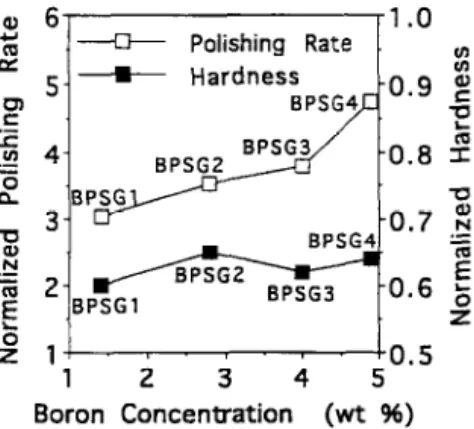
Fig. 2 shows the changes in CMP polish rate and hardness of PECVD glass as a function of phosphorus doping level. It can be inferred that the polishing rate increases with phos- phorus content, which agrees with previous reports [ 7,9]. Fig. 3 shows the dependence of the normalized (with respect to thermal oxide) polishing rate and hardness of BPSG films on boron concentration. It can be seen that lower boron level combined with higher phosphorus content in the BPSG film results in lower polish rate.
From Fig. 2 and Fig. 3, boron and phosphorus doping appears to have no significant effect on the hardness of these PECVD films, but we find that PECVD oxide, with its more open structure, has a lower hardness value than does thermal oxide. Our previous work [ IO] proposed that there is a linear
5 4 u --+3-- Polishing rate ---+-- Hardness 1.0 VI S 0.9 2 Z 0.8 = ‘0 0.7 i w E 0.6 5 0.5 012345 6 Phosphorus Concentration (wt %)
Fig. 2. Effect of phosphorus concentration of CMP polishing rate and hard- ness of PECVD glass. Both polishing rate and hardness data are normalized with respect to values for wet thermal oxide.
1 2 3 4 5
Boron Concentration (wt %)
Fig. 3. Normalized (with respect to wet thermal oxide) CMP polishing rate and hardness versus boron concentration in BPSG films.
relationship between hardness and polishing rate for undoped dielectric films, while for doped films, no distinct relationship can be drawn. The difference probably results from the chem- ical reaction for doped films, which play at least an equal role as the mechanical factor (e.g. hardness) in determining CMP polishing rate.
Cook [ 111 has reviewed the chemical processes in glass polishing. It is proposed that the water in the slurry chemically reacts with silicon dioxide. The reaction proceeds as follows: &i-0-Si= + HZ0 e 2-Si-OH
However, the diffusion coefficient of water in silica, which is believed to be the rate-controlling factor of this reaction, is quite low. For a multicomponent glass such as BPSG, the diffusive exchange of molecule (e.g. boron, etc.) into the surrounding water proceeds at a higher rate, leading to the formation of hydroxyls:
R+(glass) +HzOoH+(glass) +ROH
This molecular transport can explain that the water diffusion rate in borosilicate glass is an order of magnitude higher than for vitreous silica, and may be a good reason why chemical reaction is important for doped films during the CMP process. Also, the phosphorus incorporated in the PSG films may act as bridging atoms or interposed atoms, or they may exist in forms of P,O, and PH3 molecules which loosen the structure of the host SiOZ network [ 121. Thus, increasing the phos- phorus concentration results in faster polish.
For BPSG films, B,O, and P,O, work as impurities in the SiOZ network, and the amount of impurity affects the prop- erties of the BPSG film [ 1,2]. As compared with phosphorus
(in Fig. 3), boron seems to be the more important dopant which affects the polishing rate for BPSG films, hence, an increase of boron concentration leads to higher polishing rates even though the phosphorus content is reduced.
3.3. CMP of patterned wafer
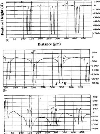
Fig. 4 shows the surface profiles of the patterned BPSG structure in the process of polishing. The scan length is 500 km. Fig. 4(a) shows that the original step height on the silicon wafer is 7000 A. In the intermediate of polishing (Fig. 4(b)), CMP tends to erode in structure with small pattern factors (i.e. the ratio between the feature area and total area) [ 131. The uneven polishing rate appearing for varied pattern width is not a surprise since the polishing rate of elevated pattern is determined by local pressure, which is inversely proportional to its polish area under a constant force.
Moreover, an unbalanced force which breaks the materials off the feature is established at different points of a feature, hence, polishing rate differs profoundly from edge to center of a feature. Runnels [ 141 has proposed that the erosion rate in the normal direction at a point on the surface is a function of the magnitude of the normal and tangential stress at that point. Since the stress at the edge of a feature is the largest
C.-W. Liu et ul. /Thin Solid Films 270 (1995) 607411
Fig. 4. The evolution of surface contour for patterned BPSG structure, (a) before, (b) intermediate, and (c) end of polishing.
among all points in the feature, the removal of material at this point is faster than other points of a feature. Thus, experiment results show a eroding feature with more and more rounding until an equal stress distribution at each point of a feature is reached. At the end of the polish, a more planar surface than the surface of reflowed films is obtained. The height variation over this scan range is less than 60 nm (Fig. 4(c)
)
Although a BPSG structure can obtain a good planar sur- face after polishing, it consumes much more materials since the removal selectivity between the up feature and recessed area is small. Many researchers [ 15,161 try to solve this problem with polish stop layers which have high selectivities to the material to be removed. In this work, we use SRO as a stop layer on a BPSG structure.
Fig. 5 shows the evolution of the surface contour for a patterned SRO/BPSG structure: before, intermediate and after polishing. Fig. 5 (a) shows that the original step height on the silicon wafer is also 7000 A,, which is same as that of BPSG structure. Initial polishing removed the top SRO film completely, exposing the BPSG, but the lower SRO remains unpolished. Since BPSG polishes faster than SRO, the BPSG level was selectively polished. Also, because the side walls are protected by the hard layers, bump shape occurred in structure edge with large pattern factors at the intermediate stage of polishing (A and B in Fig. 5(b)). This feature is
Fig. 5. The evolution of surface contour for patterned SRO/BPSG structure, (a) before, (b) intermediate, and (c) end of polishing.
clearly different from the rounding feature of the BPSG struc- ture (Fig. 4(b) ) , which does not have a stop layer.
After the completion of the process with over etch, a planar surface is also obtained (Fig. 5(c)). It is important to note that a special feature, i.e. inversion patterns, is first observed (A’ and B’ in Fig. 5 (c) ). The formation of inversion pattern is the consequence of the pad cloth being in contact with both the BPSG and the lower stop layer (A’ and B’ in Fig. 5 (b)
) .
Since the stop layer has a lower polishing rate, it will be conserved in its location and the BPSG around it will be further polished during the over etch period, this leads to the formation of an inversion pattern. These results enable us to use the inversion phenomenon for monitoring. The CMP process as an end point detection, which is still an issue for CMP process adopted in manufacture sites.4. Conclusions
The polish behavior of PSG and PBSG film is dependent
on phosphorus and boron contents in these PECVD films. FTIR was utilized to characterize these films. The polish rate was found to increase with increasing phosphorus content in PSG, and to increase with increasing boron content in BPSG although phosphorus content is decreased. On the other hand, it is observed that there is no explicit relationship between
C.-W. Liu et al. /Thin Solid Films 270 (1995) 607611 611
hardness and doping level of these doped films. From plan- arizing patterned wafer, we observed excellent surface pla- narity accomplished by CMP for patterned wafer with and without a stop layer. It should be emphasized that an inversion pattern is observed on the SRO/BPSG structure at the com- pletion of CMP process with over etch, this phenomenon is important since it can be used as a polish endpoint index for CMP process.
Acknowledgements
The authors express appreciation for helpful discussions with Dr. T.Y. Yen. This work is supported by National Sci- ence Council and TSMC (NSC84-2622-E009-007)) Repub- lic of China. The sample were prepared by United Microelectronics Company (UMC) . The doping contents
was analyzed in Winbond Electronic Company. The hardness measurements were made possibly by the assistance of the Precision Instrument Development Center for providing the NANOTEST 500 in this experiment.
References
[l] W. Kern and G.L. Schnable, RCA Rev., 43 (1982) 423. [2] I. Avigal, Solid Slate Technol., October (1983) 217.
[3] A. Takamatsu, M. Shibata, H. Sakai and T. Yoshimi, J. Electrochem. Sot.. 131 (1984) 1865.
[4] S. Wolf and R.N. Tauber, Silicon Processingfor the VLSil Era, Vol. 1, Lattice Press, CA, 1986, p. 188.
[5] S. Sivaram, H. Bath, R. Leggett, A. Maury, K. Monnig and R. Tolles, Solid Stare Technol.. May (1992) 87.
[6] P. Singer, Semicond. Int., February (1994) 48.
[7] S. Pennington and S. Lute, Proc. 9th International VMIC, 1992, p. 168.
[8] M.F. Doemer and W.D. Nix, J. Mater. Res., 1 (1986) 601.
[9] W. Ong. S. Robles, S. Sohnand B.C. Nguyen, Proc. 10th Infernational VMIC, 1993, p. 197.
[lo] B.T. Dai, C.W. Liu and C.F. Yeh, Proc. Zth International DUMIC, 1995. p. 149.
[ 1 l] L.M. Cook, J. Non-Cryst. Solids, I20 (1990) 152.
[ 121 C. Pavelescu and C. Cobianu, Thin Solid Film, 196 ( 199 1) 35 1. [ 131 P.A. Burke, Proc. 8th International VMIC, 1991, p. 379. [ 141 S.R. Runnels, J. Electrochem. Sot., I41 (1994) 1900.
[15] S. Kishii, H. Horie, M. Hoko, Y. Arimoto and T. Ito, Extended Abstracts of the 1993 International Conference on Solid State Devices and Materials, Makuhari, 1993, p. 189.
[16] B. Neureither, C. Basa, T. Sandwick and K. Blumenstock, J. Electrochem. Sot., 140 (1994) 3607.