A Cost-Effective Preamble-Assisted Engine With
Skew Calibrator for Frequency-Dependent I/Q
Imbalance in 4
4 MIMO-OFDM Modem
Wei-Chi Lai, Yuan-Te Liao, and Terng-Yin Hsu, Member, IEEE
Abstract—Variations in I/Q gains, phases, and filters of the RFfrontend, namely frequency-dependent I/Q imbalance (FDI), are an important factor in OFDM-based wireless access. To enable the proper function of a 4 4 MIMO-OFDM receiver this work proposes a low-complexity preamble-assisted solution using only one complex divider and one complex multiplier to handle signifi-cant FDI distortions. An all-digital multiphase and multi-rate clock generator (MPRCG) was built to support fast dynamic frequency scaling for FDI estimation and compensation and for efficient im-plementation. Based on the proposed MPRCG, a skew calibration was also realized to tune I/Q timing coherently via multiphase A/D clocking. Performance evaluation showed that the proposed ap-proach incurs an SNR loss of 1.5 dB to maintain a packet-error rate of less than 10% under a 1 dB gain error, 15 phase error and worse filter mismatch. Thus, this solution not only provides ade-quate performance, but also makes FDI estimation and compensa-tion more cost-effective.
Index Terms—Clock generator, dynamic frequency scaling,
fre-quency-dependent I/Q imbalance, I/Q mismatch, MIMO-OFDM.
I. INTRODUCTION
M
ULTIPLE-INPUT multiple-output orthogonal fre-quency division multiplexing (MIMO-OFDM) is widely used in next-generation communication systems to overcome frequency-selective fading [1]–[3]. However, RF distortions result in serious degradation in performance for most OFDM-based systems. Mismatches in gain, phase, and filter between in-phase (I) and quadrature-phase (Q), known as frequency-dependent I/Q imbalance (FDI), cause not only time-domain signal skew but also frequency-domain gain and phase imbalance. As a result, it becomes difficult for an OFDM direct-conversion receiver to recover data. The goal of this study is to mitigate analog front-end imperfections such as FDI distortion via digital signal processing.A huge number of schemes have been proposed for such impairment compensation (e.g., [4]–[20]). Some studies [4]–[9] Manuscript received January 31, 2012; revised July 11, 2012; accepted November 04, 2012. Date of publication February 01, 2013; date of current version July 24, 2013. This study was conducted under the “Advanced Wireless Broadband System and Inter-networking Application Technology Develop-ment Project” of the Institute for Information Industry, which is subsidized by the Ministry of Economic Affairs of the Republic of China, and is supported in part by the Taiwan Semiconductor Manufacturing Company and in part by the National Science Council of Taiwan, under Grant NSC100-2220-E-009-040 and NSC100-2220-E-009-028. This paper was recommended by Associate Editor J. Ma.
The authors are with Department of Computer Science, National Chiao Tung University, Hsinchu 300, Taiwan (e-mail: tyhsu@cs.nctu.edu.tw).
Color versions of one or more of the figures in this paper are available online at http://ieeexplore.ieee.org.
Digital Object Identifier 10.1109/TCSI.2013.2239431
utilized specific formats in SISO-OFDM systems. A post-FFT least-squares equalization [4] costed 40 training symbols to achieve -dB SNR loss. Based on signal correlation property, a time-domain least-squares method [5] ensured low compu-tational complexity. With loopback signal path, an adaptive pre-distortion scheme [6] required 1000 independent trials to reach at least 50-dB image rejection ratio (IRR). By using trigonometric least mean square algorithm, a CORDIC based adaptive FIR filter [7] worked properly within 20 iterations. In order to perform over 70-dB IRR, a pilot-based self-calibration approach [8] averaged 100 estimation results in the TX and the RX, respectively. And a nonlinear least squares scheme [9] would estimate both CFO and FDI within 1-dB SNR loss. In MIMO-OFDM systems, the joint compensation of CFO, TX FDI and RX FDI [10], whose SNR loss was less than 1 dB, was also performed by the user-defined preamble. Because IEEE WLAN standards define the short, long preambles (training fields) and coded datum, the I/Q imbalance can be solved efficiently. For ex-ample, a low-complexity time-domain algorithm [11] was used and implemented in an IEEE 802.11a receiver (SISO OFDM). And a few solutions were derived for IEEE 802.11n systems (MIMO OFDM): (1) a linear optimal solution and an RLS-based adaptive filter [12]; (2) an input-output relation governing Alamouti-coded OFDM systems [13]; and (3) a cross-validation estimation via the property of long preambles [14]. Recently, the blind algorithms have been made for general SISO-OFDM systems, e.g., a self-calibrating image rejection scheme [15]
with an dB, a CSAD method [16] for both CFO
and FDI, an adaptive Wiener filter [17] for FDI cancellation, one time-domain and one frequency-domain FDI estimations [18] via the second-order statistics, a joint estimation and com-pensation [19] of CFO and FDI under timing uncertainty, and a circularity-based FDI compensation [20] being independent of carrier synchronization. Although several approaches [15], [17]–[19] work properly, they require at least 4000 trials to converge, and cost over 10 k multiplications and 20 k additions. This study proposes a relatively low-complexity pre-amble-assisted algorithm, which has a cost-effective imple-mentation and is able to remove FDI distortions in a 4 4 MIMO-OFDM receiver. Only four short and four long pream-bles are needed to estimate FDI distortions over frequency domains. Through skew calibration, the filter mismatch can be reduced to enhance frequency-domain compensation. Our implementation consists of a preamble-assisted engine, and an all-digital multiphase and multi-rate clock generator (MPRCG), as shown in Fig. 1. The proposed MPRCG not only eliminates timing skew via multiphase A/D clocking, but also supports fast dynamic frequency scaling (DFS) to minimize the number of complex dividers and complex multipliers in the 1549-8328/$31.00 © 2013 IEEE
Fig. 1. Block diagram of a preamble-assisted engine with skew calibration for frequency-dependent I/Q imbalance.
preamble-assisted engine. As a result, the proposed mechanism is cost-effective and is well-suited to the next-generation wire-less LAN proposed in the IEEE 802.11 TGac [22] group, as it uses only one complex divider and one complex multiplier.
The rest of this paper is organized as follows. Section II addresses system assumptions and mathematical notations. Section III presents the proposed preamble-assisted I/Q compensator. The hardware implementation is described in Section IV. Section V discusses the performance evaluation. Conclusions are presented in Section VI. Finally a divider-free arc-tangent and a table of abbreviations are presented in Appendix.
II. SYSTEMASSUMPTIONS
A. System Description
This MIMO-OFDM system is set up for point-to-point trans-mission, e.g., an infrastructure mode, as shown in Fig. 1. A close-loop pre-compensation scheme is applied to account for CFO. A pseudo-CFO (P-CFO) [23] method, which rotates three training symbols by adding an extra frequency offset into the re-ceived sequence, is used to obtain an accurate CFO value under I/Q mismatch. Having found this value, the transmitter can adjust its carrier to pre-compensate for the CFO distortion. Each MIMO-OFDM symbol has sub-carriers where sub-carriers are data and pilots. The other sub-carriers are nulls. The packets are assumed to contain common preambles and MIMO preambles, where the common preambles are similar to the preambles in SISO-OFDM systems. Both common pream-bles and MIMO preampream-bles can be of two types: 1) time-domain short preambles, such as the common short preamble (CSP) and the MIMO short preamble (MSP); and 2) frequency-domain long preambles, such as the common long preamble (CLP) and the MIMO long preamble (MLP). The term
denotes the th CSP symbol in the th transmitter antenna and its
valid length is , where . The term
represents the th MLP symbol in the th trans-mitter antenna and represents the th fraction (sub-carrier). The number of MLPs is equal to the number of transmitter antennas, and their length is equal to . The detail descriptions of mathematical notations are provided in Table I.
B. FDI Models
Fig. 2 shows the block diagram of a typical FDI model [9], [14], [18]. The received RF signal with a central frequency is expressed as
(1)
TABLE I
TABLE OFMATHEMATICALNOTATIONS
where is the received baseband signal, denotes the complex conjugate, and is the index of the receiver antenna. The received RF signal is direct down-converted by a local oscillator signal with mismatched I branches and Q branches. The amplitude mismatch and phase error are
and , respectively; ideally,
and . The local oscillator signal of an
imbalanced quadrature demodulator is then given by
(2)
The down-converted signal is
as shown in (3), where and are the low-pass filters for the I and Q branches, respectively. The frequency responses
of and are given by and ,
re-spectively The non-coherent and result in timing skews that are caused by the inconsistent main pulses of two
Fig. 2. Model of frequency-dependent I/Q imbalances in MIMO-OFDM systems.
LPFs, which are plotted in Fig. 3(a) and (b). From (3), the fre-quency-domain I- and Q-path signals after low-pass filtering are given by (3)–(4), shown at the bottom of the page. Thus, the
re-ceived down-converted signal is
(5) where
(6) and is the received baseband signal in the th receiver antenna, and is the image aliasing effect due to
I/Q distortions where is the mirror
po-sition (sub-carrier) of the OFDM symbols. For simplification without loss of generality, these two LPFs can be modeled by a finite impulse response (FIR) filter [9]. For example, the filter mismatch can be modeled by a worse case [9] of
and , or as a
minor case of and
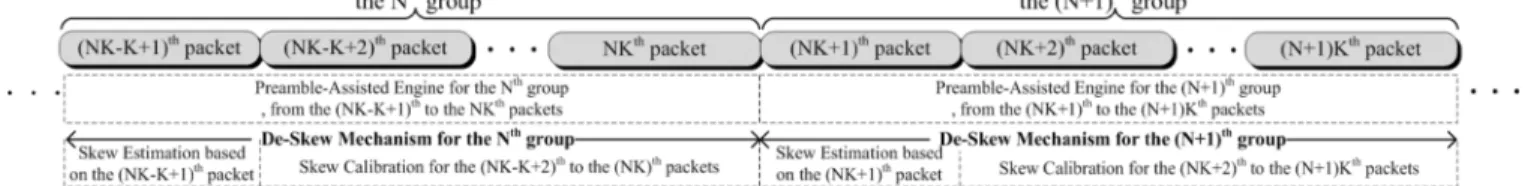
, as shown in Fig. 4(a) and (b). These also show that filter mismatch and its timing skew cause severe dis-tortions. Due to the process, voltage and temperature effects of RF parts, FDI distortions are modeled as quasi-static, allowing distortions to be time-invariant over one group, composed of K packets , and change dependently from group to group.
Fig. 3. Timing skews between the I and Q paths: (a) skewed by half a sample period and (b) skewed by one sample period.
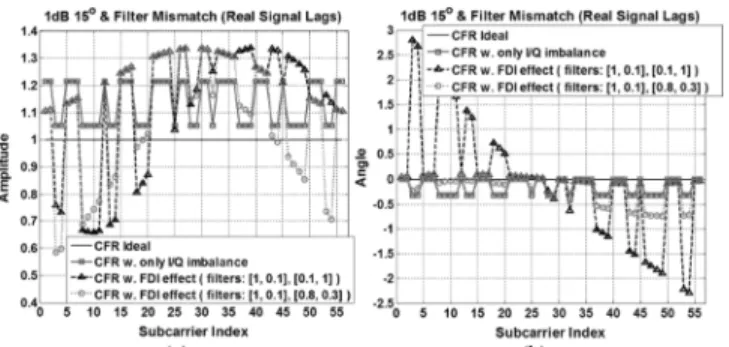
Fig. 4. Amplitude and angle of channel frequency response with 1 dB gain error, 15 phase error and timing skew: (a) amplitude and (b) angle.
C. Problem Statement
For a cost-effective design, preambles are useful to reduce computational complexity. If such preambles (e.g., the CLP and the MLP in the specifications) are not well-defined in packets, we can create a virtual one via the received preambles. Since the timing skew of filter mismatches cause I-path and Q-path signals inconsistency, as shown in Fig. 3(a) and (b), it should be eliminated first to reduce the residual I/Q-imbalance. Yet, it is difficult to remove that distortions by shifting or skewing I-path or Q-path buffers after analog-to-digital (A/D) conver-sion. Using multiphase A/D clocking to skew A/D sampling is simple and useful for making the main pulses of I-path and Q-path LPFs coherent. Besides, the number of complex dividers and complex multipliers must be minimized due to the high
(3)
Fig. 5. The cross-ratio imparity of and .
Fig. 6. Steps of the proposed mechanism.
cost of these two components in VLSI design. And multi-rate clocking should be utilized because the computational effort required for FDI estimation and compensation ([16], [17] and [18]) is not the same. Although phase-locked loops (PLL) and delay-locked loops (DLL) are popular, most exhibit unexpected phase transients, known as the hang-up phenomenon [24]–[26]. It is also key to derive an all-digital multiphase and multi-rate mechanism without PLLs, DLLs and analog circuits requiring.
III. PREAMBLE-ASSISTEDCOMPENSATION
A. Basic Concept
Due to the image aliasing effect caused by I/Q distortions shown as (5), a cross-ratio imparity (CRI), , is de-fined to serve the extraction of I/Q imbalance where
is the difference between the ratio of th symbol of preamble to its conjugate mirror part, and the ratio
of th symbol of preamble to its
conju-gate mirror part, where and
(7)
where and are two
different frequency-domain preambles in the th transmitter antenna. According to heuristic results, at least one quarter
of and should satisfy
and be distributed uniformly to ensure accurate FDI estimation. Therefore, we collect time-domain CSPs and transfer them to the frequency domain via FFT to get a virtual long preamble (VLP), which is defined by
(8) where
where denotes the coefficient of the FFT, and sig-nifies the transpose of the matrix. Then the from (7) can be rewritten as follows:
(9)
Fig. 5 shows plots of and ,
where is distributed uniformly. To
ex-tract all the mismatches of gains, phases, and filters, a
CRI, , is required, where is
defined as
as (9). Since the multiphase A/D clocking is able to calibrate the skew of the two main pulses of I-path and Q-path LPFs to reduce filter mismatches, the proposed algorithm is divided into two parts: 1) CRI-based estimation to deal with FDI distortions via
over the frequency domain and 2) skew calibration to improve performance. However, most MIMO-OFDM systems do not support enough preambles for these two techniques to be applied to the same packet simultaneously. We can remove the skew of the two main pulses of the I-path and Q-path LPFs by using the skew information from the previously received packet. Thus, the SNR needed for the CRI-based estimation can be efficiently reduced. The steps of the proposed work are shown in Fig. 6. The first packet of every group estimates such skew information. Skew calibration, residual IQ-imbalance estimation and compensation are then active from the second packet to the th packet per group.
B. CRI-Based Estimation
Since the can be developed to satisfy
as shown in Fig. 5, we can estimate FDI distortions over the frequency domain. The channel frequency response (CFR) between the th transmitter antenna and the th receiver
antenna can be estimated by multiplying
the received and the inverse matrix of ideal
CFR is a function of and
the ratio of and its conjugate mirror
(10)
where and are the parameters of the FDI
distortions in the th receiver antenna, and is the ideal estimated CFR of frequency-selective fading in each path,
where . The received virtual long
pre-amble in the 1st receiver antenna is equal to the
summation of .
Ac-cording to the FDI model in (5), the received virtual long
pre-amble becomes
(11) Based on (9),
can replace in
(11), which becomes (12), shown at the bottom of the page. After replacing
with from (10), can
be reduced as follows:
(13) In order to eliminate the unknown quantity
in (13), we use (9) and (11) again. First, we replace index with and by taking the conjugate of (9) shown as in (14),
is
equal to .
(14)
Replacing with
in (11), we get (15), shown at the bottom of the
page. The from (10) can substitute for
in (15). Thus, (15) becomes
(16)
To remove the unknown values in (16) and
in (13), we replace index with and take the conjugate of (16), which can be expressed as
(17) where
. Since are
known, can be defined as
. The
in (13) and (17) is canceled by division. The ratio of
to is defined by the in
(18), at the bottom of the next page, where
. However, this representation of is insufficient due to the limited number of samples of the received preambles with . For example, only one-quarter of the sub-car-riers (12 sub-carsub-car-riers) are available to measure the in 802.11n [21]. The remaining ratios must be determined by linear interpolation with moving-average smoothing in the frequency domains. The FDI compensation is then determined by
(19)
(12)
To reduce hardware complexity and decrease latency, a divi-sion-free compensation is found as follows:
(20) where
and is the desired data. Because is just
a part of the equivalent linear channel, and the radio channel can be equalized together. is then determined after equalization. In addition, this division-free compensation only requires one multiplication and one sub-traction operations per subcarrier.
C. Skew Calibration
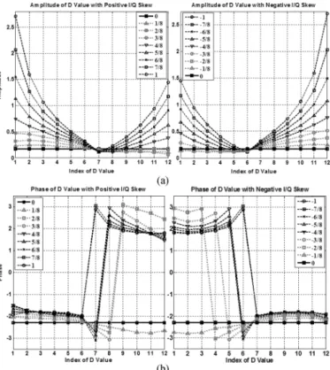
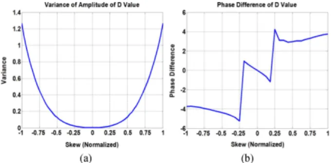
In order to improve IRR and reduce the required SNR, a skew calibration is proposed to reduce the timing mismatch of the two main pulses of LPFs via multiphase A/D clocking. The es-timated in (18) varies with frequency due to the mis-match in the filters, gains, and phases, as shown in Fig. 7. The normalized I/Q skew is from ideal sampling to ideal sam-pling in the TGnD channel (8 taps and 50 ns RMS delay spread) [27] and FDI distortions with a 1 dB gain error and a 15 phase error [9], [14]. The I/Q skew is negative when the Q-path signal leads the I-path signal, and positive when the Q-path signal lags the I-path signal. From Figs. 7(a) and 8(a), it is also clear that the variance in amplitude increases as skew increases. Fig. 8(a) also shows that the variance is almost zero if the absolute value of I/Q skew is less than 0.25. The absolute value of residual I/Q
skew of the th group is acquired via the
th packet , where
given in
(21) where
is the estimated residual I/Q skew of the 1st receiver antenna in the th group, and is the mean of
; the function is used to
determine based on the heuristic thresholds
. Fig. 7(b) shows the phase of the 12 estimates
Fig. 7. Amplitude and phase of D value with the TGnD channel, 1 dB gain error, and 15 phase error: (a) amplitude and (b) phase.
for and Fig. 8(b) shows the
phase difference between
and . From these figures,
we know that the sign of residual I/Q skew is the same as the sign of
when its absolute value is greater than or equal to 0.25. Since we only need the absolute value of residual I/Q skew to be greater than or equal to 0.25 in (21), the sign of the estimated residual I/Q skew
is
(22) From (21) and (22), the estimate of residual I/Q skew can be determined. The skew
informa-tion of the th group is obtained from
(23)
Fig. 8. Characteristics of D values: (a) variances of amplitude and (b) phase difference between (12) and (1).
where is the skew information of the Nth
group. For the th receiver antenna, the same steps are applied to eliminate FDI distortions. Only 4 CSPs and 4 MLPs are required for the proposed solution.
IV. HARDWAREIMPLEMENTATION
The proposed hardware implementation is a 4 4 MIMO-OFDM receiver that meets the IEEE 802.11n draft requirements [21]. Two main components are described: 1) a preamble-as-sisted engine and 2) a multiphase and multi-rate clock gener-ator. Their architecture is described in detail.
A. Preamble-Assisted Engine
The key to developing low-complexity implementations is to use only one complex multiplier and one complex divider shared among four antennas in RX. Fig. 9 shows the VLSI ar-chitecture of the proposed solution. This preamble-assisted en-gine performs three major functions: 1) estimation of the skew period, 2) estimation of residual FDI distortion and 3) compen-sation for the residual FDI. As complex dividers and complex multipliers account for most of the gate count in the implemen-tation, a high-speed inner clock is needed to reduce the quantity of these two components by implementing a shared architecture. Since the computational effort involved in FDI estimation and compensation is different ([16], [17] and [18]), this high-speed inner clock needs to quickly switch between different clock rates for estimation and compensation for high power efficiency. Fur-thermore, both the ROM bank and the RAM bank are required to store data for each receiver antenna. The details of operation are as follows.
First, the estimated CFRs and received preambles become complex conjugates through the D-type latch. The ideal
pream-bles (frequency domain and are
pre-stored in a ROM bank. The numerator and denominator of the , which are obtained using (18), are stored in a RAM bank. Thus, by using a complex divider, the
can be determined for the skew period estimation. As only 12 sub-carriers are able to calculate the directly using the received preambles in 802.11n [21], the other 44 sub-carriers must be determined using the linear interpolator. Instead of a divider, this linear interpolator only needs shift registers because has non-zero values in the
posi-tions and (shown in Fig. 5). Then
a moving average process is exploited to smooth the whole which is for FDI compensation. The cost of this
division-free compensation is just one multiplication and one subtraction per subcarrier based on (20).
According to (21) and (22), the absolute value of estimated
skew is determined by the variance of and the
sign of estimated skew is decided by the phase of
using the divider-free arc-tangent unit, shown in Appendix A. In Fig. 9, are the statistical results used as the boundary to determine the absolute value.
Once the timing skew of th group is
cal-culated, the multiphase A/D clocking will skew the A/D sam-pling to make main pulses of the I/Q signals coherent from the
th to the th packets.
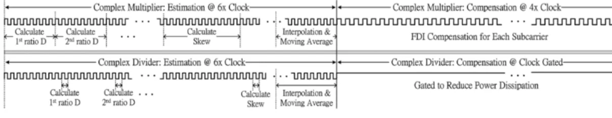
To reduce complexity, only one complex divider and one complex multiplier are employed in the proposed engine. To perform FDI estimation based on (18), we need 8 multiplica-tions, 1 division and 8 additions/subtractions to calculate each involves 108 multiplications/divisions and 96 additions/subtractions and). In addition, another 14 mul-tiplications/divisions and 36 additions/subtractions are needed to determine the skew estimate . Using linear in-terpolation and moving averages, the total number of multiplica-tions/divisions and additions/subtractions required are 176 and 294, respectively. The process flows of the complex multiplier and the complex divider are shown in Fig. 10. A 6 clock is re-quired to share one complex multiplier and one complex divider for FDI and skew estimations because there are 80 sub-carriers ( cyclic prefix) per OFDM symbol. Thus, 480 (80 6) cycles are available to process ratio calculation, skew estima-tion, linear interpolation and the moving average. For FDI com-pensation, a 4 clock is adequate for the complex multiplier because only one multiplication and one subtraction are needed per sub-carrier (based on (20)). Since division operations are not required for compensation, the unused complex divider should be gated to reduce power dissipation. Therefore, the required clock rates of the proposed engine are and 0. DFS is implemented to improve the power efficiency and minimize the area (memory) requirements of the shared architecture. How-ever, PLL-based DFS does not provide a -to- fast DFS because the switch time of the FDI estimation and compensa-tion is critical. An all-digital multi-rate mechanism is derived to make it easy to integrate DFS in a 4 4 MIMO-OFDM modem.
B. Multiphase and Multi-Rate Clock Generator
1) Four-Phase Clocking: In order to reduce filter
mis-matches via multiphase A/D clocking, a four-phase clock is needed to calibrate the timing skew of two main pulses of LPFs according to (21) and (22). While the phase interpolator [28] without PLL and DLL is a useful scheme for generating multiphase clocks, the analog delay elements are difficult to implement for wideband operations. Fig. 11 shows the all-dig-ital architecture of the proposed MPRCG. The clock A2 has a phase delay of 180 in relation to clock A1. The clock OUT0 has a phase delay of in relation to clock A1, set using a programmable all-digital delay line. Clock A3 has a phase delay of . The interpolator will create clock OUT90, which has half the phase delay of clock A2 in relation to clock A3. Therefore, the phase delay between clocks OUT0 and OUT90 is almost 90 . From OUT0 and OUT90, four clock with phase
delays of and can be
Fig. 9. The architecture of the preamble-assisted engine for a 4 4 MIMO-OFDM modem.
Fig. 10. The process flows of the complex multiplier and the complex divider.
Fig. 11. Architecture of the all-digital multiphase and multi-rate clock generator. time-to-digit converter (TDC) to calculate the cycle period of the input clock, programmable all-digital delay lines to set an appropriate delay, and the interpolator to generate a half-phase delay between two input clocks and a control unit to control the programmable all-digital delay lines. To reduce timing mismatches and provide good controllability, the delay chain applied in the TDC is also utilized in two all-digital delay lines and a dual-loop digitally controlled oscillator (DCO). To achieve good phase interpolator performance, the phase delay between clocks A1 and A3 is set as 150 –180 . The details of operation are as follows.
First, a TDC that includes a delay chain and a cascaded counter is employed to measure the period of the input clock. When it operates, the delay chain starts at the positive edge
Fig. 12. Post-layout simulation of the four-phase clock generator at 80 MHz.
of the half-input clock and the D-type flip-flops record the delays to digitize the input period at the falling edge of the
Fig. 13. Post-layout simulation of the multi-rate clock with a 20 MHz input clock for and 6.
half-input clock. Then, the control unit processes the input period to control the programmable all-digital delay line, which can delay the input clock by . Each programmable all-digital delay line is composed of four parts: a differential circuit for creating pulses on each edge of the input clock, a pulse-trigger monostable delay amplifier for delaying the input signal for -round inner loops, a divide-by-2 divider for re-generating the output clock, and an individual delay chain used to enhance the resolution. Since each AO21Dx cell provides a few picosec-onds of resolution in the monostable delay amplifier, a counter is employed to count the number of rounds of the inner loop to reduce the hardware cost and maintain flexibility. When the counter ends its count, signal S2 is set high to clear the D-type flip-flop. Next, signal S3 from the port of the D-type flip-flop will become high to stop the inner loop and reset the counter to zero. The delay cell D2 increases the driving capability of the signal S3. The delay cells D3–D6 delay the reset signal S3 to prevent a glitch in signal S2. On reset, the counter will set signal S2 to low to stop the reset signal S3. Thus, the counter causes signal S2 to become a pulse signal. Next, a divide-by-2 divider scales the output frequency by half, making it the same as the input clock. Finally, the individual delay chain improves the resolution according to the control signal C0–C2 . To balance hardware cost and circuit delay, the value of is 5 (resulting in a 32-stage TDC, delay amplifier, and individual delay chain). Fig. 12 shows a post-layout simulation of four-phase clock generation in an in-house 65 nm 1P6M digital CMOS process. The power dissipation is 289 W at 160 MHz with a 1.0 V supply voltage.
2) Multi-Rate Clocking: To efficiently utilize the single
complex multiplier and single complex divider for the dissim-ilar operations of estimation and compensation, a fast-switch multi-rate clock ( clock rate) is provided by an all-digital MPRCG, which is built without any analog and all-digital PLL, as shown in Fig. 11. The proposed multi-rate clock generator consists of a time-to-digital converter (TDC) that is shared with the four-phase clock generator and calculates the input cycle period, a divider that calculates multiplied by the input clock period, a dual-loop DCO for wideband transmission, and a counter that enables or disables the output of the dual-loop DCO. After TDC, a programmable divider calculates the clock
period of an ( times the input
clock period). Since is either 4 or 6 in our implementation, this divider is implemented using shifters, an adder, and a subtractor. The subtractor is used to calculate the approximate
clock period of an as follows:
(24) where is the period of the input clock, is the frequency multiplication factor, is the clock period of the high-speed clock and is a tolerance factor representing mis-matches of circuits and layouts ( for an in-house
65 nm CMOS digital process). If is equal to 4, only a shifter is needed. If is 6, the calculation can be implemented
by . Thus, only
shifters and an adder are needed.
After the divider, a dual-loop DCO begins to generate an high-speed clock, and the counter maintains the “window” signals [29] (Fig. 11), which allow the dual-loop DCO to gen-erate clocks at each rising edge of the input clock and to disable the dual-loop DCO after clocks. The dual-loop DCO consists of two parts: 1) an inner loop for extending bandwidth and 2) an individual delay chain for increasing resolution. In order to minimize gate count and provide flexibility, a counter is utilized to calculate the number of rounds in the inner loop ( stages for each round). Next, the individual delay chain (con-trolled by the signal C’0-C’2 ), is used to improve the resolu-tion of the dual-loop DCO. Due to the inner loop and individual delay chain, the dual-loop DCO is able to output a fast-switch multi-rate clock at the positive edge of the window signal. The differential circuit is utilized to generate pulses on rising or falling edges of the signal S1 in order to reset the counter to zero. A Schmitt trigger buffer cascaded with two clock buffers is added at the output to reduce jitter and enhance the driving capability because this multi-rate clock must drive the proposed preamble-assisted engine. The clock buffer D1 before the output isolates the feedback clock and reduces loading effects.
Since it employs AO21Dx logic to control the clock feed-back (a total of stages), the dual-loop DCO is not affected by large parallel loading and long reset latency, in contrast to tri-state feedback [30] and pass-transistor feedback. There are 32 stages in each delay chain and the counter counts every 2 rounds, like the TDC and the delay amplifier. Using the proposed all-digital MPRCG, an approximate high-speed clock can be created easily and synchronized at each rising edge of the reference clock without PLLs. The main cost of applying this MPRCG is a 10–15% additional timing margin in VLSI implementations. Fig. 13 shows the post-layout simulation of the -to- clock and fast switching with a 20 MHz
refer-ence clock. According to (24), with and , the
clock runs at 79.62 MHz and the frequency offset is 0.48% (compared to 80 MHz). The clock is at 122.25 MHz and the frequency offset is 1.88% (compared to 120 MHz), with and . Both of these results are well within the 15% timing margin.
C. Implementation and Discussion
All modules, including the preamble-assisted engine, the MPRCG, and the divider-free arc-tangent (Appendix A) were realized using hardware-description language and Design An-alyzer (Synopsys). Our work was implemented by the Taiwan Semiconductor Manufacturing Company in-house 65 nm 1P6M GP CMOS technology. The hardware costs of the proposed solution can be divided into two components: the base part that is independent of the RX antenna numbers; and the MIMO part,
TABLE II
VLSI COMPLEXITY OF THEPREAMBLE-ASSISTEDENGINE
which is proportional to the RX antenna number; this data is summarized in Table II. The base part consists of six mod-ules that cost 27.6 k gates (60.4%): 13.4 k gates for a complex divider, 6.1 k gates for a complex multiplier, 3.4 k gates for the proposed divider-free arc-tan, 2.7 k gates for 16 complex adders, 1 k gates for 5 comparators and 1 k gates for an en-coder. The MIMO part includes 22 multiplexers, a control unit, an address generator and D-latch conjugates, and occupies 14.2 k gates (31.07%). The MPRCG with 32 stages in each delay chain is composed of a TDC (1154 gates), a control unit (988 gates), two programmable delay lines (968 gates), a dual-loop DCO (495 gates), a divider that divides by 4 or 6 (116 gates), a counter (103 gates), an interpolator (16 gates) and other parts (64 gates). The output range of the proposed MPRCG is from 3.2 MHz to 7 GHz. The total gate count including both the preamble-assisted engine and the MPRCG is 45.7 k.
As multi-rate clocking uses the TDC shared with the four-phase clock generator, it only costs an additional 714 gates (including a divide-by-4-or-6 divider, a dual-loop DCO and a counter). With multi-rate clocking, the preamble-assisted engine only needs one complex divider (13.4 k gates) and one complex multiplier (6.1 k gates). Thus, the extra 714 gates help save on an additional gate count of 19.5 k (13.4 k 6.1 k), making this architecture cost-effective. Since register buffers, RAM and ROM are necessary for sharing the proposed solution with four receiver antennas, 384 bytes of ROM and 1598 bytes of SRAM are required, which cost the equivalent of about 50k gates. Furthermore, to balance the wire loading of pro-grammable all-digital delay lines in MPRCG shown in Fig. 11 the fixed layer must be enabled in the ASIC layout to guarantee inter-connection. The MPRCG must also be placed close to the
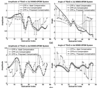
Fig. 14. Amplitude and phase of estimated CFR with a FDI of 1 dB gain error, 15 phase error and a worse filter mismatch with skew for a 1 sample period in TGnD channel: (a) 2 2 MIMO OFDM and (b) 4 4 MIMO OFDM.
power lines and power PADs to have adequate current in order to stabilize the power bounce and reduce clock jitter.
V. PERFORMANCEEVALUATION
A. Simulation and Measurement
This solution was ported to IEEE 802.11n [21],
sup-ported 1) 2 2 MIMO OFDM and 2) 4 4 MIMO OFDM,
with a bandwidth of 20 MHz (
and ), 64-QAM modulation, 2/3-coding rate, 4 4
space-time block code [31] and a data length of 1024
bytes. In addition, and
sat-isfy the condition in twelve positions
( and ). A
frequency-se-lective fading model [27] was used to evaluate the proposed approach. The two types of channel conditions consid-ered are TGnD (RMS: 50 ns, 8 taps) and TGnE (RMS: 100 ns, 15 taps) [27]. In each antenna, the settings of the frequency-dependent I/Q imbalances are 1 dB gain error, 15 phase error and a worse filter mismatch with a dif-ferent skew period [9], [14] (the LPFs of the I-path and the
Q-path are modeled as and
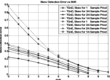
, and the skew period including a 1, 1/2, 1/4 and 1/8 sample period). The packet-error rate (PER) is the performance index and the required PER is 10%. Fig. 14 shows the amplitude and phase of estimated CFR with frequency-dependent I/Q imbalances in the TGnD, where the high-frequency distortions are removed and the CFRs are comparable to those of frequency-selective fading after compensation. Although there are gain and phase differences between compensated CFR and ideal CFR, shown as in (20), they will not degrade the performance due to being as a part of CFRs in the equalizer. Fig. 15 plots the error rate of the skew period detection. It shows that the skew-detection error rate approaches zero when SNR is greater than 10, which means the proposed skew detector
Fig. 15. The error rate of the (normalized) skew detection.
Fig. 16. PER versus SNR, with a worse filter mismatch, 1 dB gain error, 15 phase error and TGnD fading channel.
functions as required. In Fig. 16, the conditions of frequency-se-lective fading are TGnD [27]. The FDI condition is 1 dB gain error, 15 phase error and a worse filter mismatch [9], [14] with skew periods of 1, 1/2, 1/4 and 1/8 of the sample period. Fig. 16 shows the following scenarios: “FDI w. Ideal Compensation” refers to a system with perfect compensation; “FDI w/o Com-pensation” means that the compensation scheme is not applied to the system; and “FDI (skew 1/8 sample period) w/o Deskew but w. Freq.-Domain Compensation” indicates that the skew pe-riod of the FDI condition is 1/8 of the sample pepe-riod and the time-domain skew calibration scheme is not used, only the fre-quency-domain I/Q compensator is applied; “FDI w. Deskew & Time-Domain Compensation” means that after the time-do-main skew calibration scheme, a typical time-dotime-do-main I/Q pensator is used instead of the proposed frequency-domain com-pensator; and “FDI w. Deskew & Freq.-Domain Compensation” means that after the time-domain skew calibration scheme, the frequency-domain I/Q compensator in (20) is applied. Since a
Fig. 17. PER versus SNR in SISO-OFDM Platform with TGnD and a worse FDI of 1 dB 15 [5], [11], [16]–[18].
Fig. 18. SDR platform for a 2 2 MIMO-OFDM system.
1/8 skew of filter mismatches is not critical, we only consider skews of 1, 1/2 and 1/4 sample periods in the design. With both skew calibration and frequency-domain compensation, this work proposes a 1.5 dB SNR loss to ensure a % and a dB IRR per antenna. If FDI distortions are the same in every packet, then a dB IRR can also be achieved through more packets. For a robust comparison, the proposed design and other researches [5], [11], [16]–[18] were all ported to a SISO-OFDM platform in the TGnD channel (RMS: 50 ns, 8 taps) and the worse FDI of 1 dB gain error and 15 phase error. Those SNR losses are: 1) 3.5 dB [5]; 2) 0.7 dB [16], [17]; 3) 2.6 dB [18]; and 4) 2 dB (this work), as shown in Fig. 17.
For algorithmic verification, a 2 2 software-defined radio (SDR) was constructed, as shown in Fig. 18. The field-pro-grammable gate array (FPGA) chips (Xilinx Virtex-II) with on-board 14-bit digital-to-analog (D/A) and analog-to-digital (A/D) converters serve as the interface between the in-house RF modules and the software. The packets are generated using MATLAB and then transmitted to RF front-ends through 14-bit D/A convertors. In order to make MIMO transmissions coherent, an additional D/A module acts as a hardware trigger controlling all D/As coherently at TX. After down-converting the RF signals into baseband at the receiver, analog signals are fed into four 14-bit A/Ds for quantization. The proposed algorithm then processes the quantized signals using software (MATLAB). In this platform, we used MATLAB to generate skewed I-path and Q-path signals in TX for creating filter mismatch. The gain and phase errors were dB and , respectively. We employed an system clock to simulate
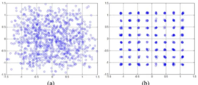
Fig. 19. Measured 64-QAM constellations in the 1st receiver antenna with 0.9 dB gain error, 10 phase error, a normalized skew period of and 50.9 dB IRR: (a) without compensation and (b) with compensation.
MPRCG in the FPGA because the FPGA cannot realize our delay chain. Carrier synchronization and channel estimation [32] have also been included. The measured 64-QAM constel-lations in the first receiver antenna at RX are plotted in Fig. 19. The measured IRR is 50.9 dB, which is better than the 47 dB in MATLAB because the channel fading in the SDR platform is much simpler than in the TGnD channel. The measured EVMs with and without compensation were dB and
dB, respectively. Both simulations and measurements suggest that the proposed 2 2 MIMO-OFDM receiver overcomes the problems of frequency-dependent I/Q imbalances, and is suitable for a 4 4 MIMO-OFDM receiver.
B. Complexity Discussion
Table III summarizes the comparison of design features in the TGnD channel (RMS: 50 ns, 8 taps) and the worse FDI of 1 dB gain error and 15 phase error, e.g., system specification, converged cycles, computational efforts, SNR losses and gate counts. By using time-domain least-squares method for FDI cancellation via known preamble [5], a total of 208 multipli-cations/divisions and 191 additions/subtractions are required in a 64 pt FFT-based OFDM system with perfect CFR. A FII is estimated via long preambles [11] requiring around 258 multiplications/divisions and 252 additions/subtractions in an OFDM system with 64 subcarriers. Taking the compensation into consideration, the total numbers of multiplications/divi-sions and additions/subtractions required are 578 and 380. Besides, two filter-based methods result in low SNR losses, but they require additional computational complexity: 1) a CSAD [16] with upsampling where the length of the de-correlating adaptive filters is 3 costs about 1848 multiplications/divisions and 1176 additions/subtractions; 2) a Wiener-based solution [17] using multiplications and matrix inverses requires over 20 k multiplications/divisions and 30 k additions/subtractions for estimation and compensation. With a single-tap matrix filter inversion, a blind-based FDI compensation [18] needs 30 000 symbols, 13 440 k multiplications/divisions and 9600 k additions/subtractions. The proposed CRI-based estimation and skew calibration require 176 multiplications/divisions and 294 additions/subtractions, including interpolation and the moving average. According to (20), 56 multiplications/divisions and 56 additions/subtractions are needed to compensate for an OFDM symbol with 56 data subcarriers. In total, each OFDM symbol requires 232 multiplications and 350 additions/subtractions to
remove FDI distortions over the frequency domain. Compared with these solutions, the proposed method needs only 4 short preambles and 4 long preambles and requires the lowest com-putational effort.
For a fair comparison of VLSI implementations, we focus on total gate counts instead of area as the chip area is affected by technology, cell library, design rules, utilization, floorplan, routing scheme, and power width. The MIMO parts of multi-plexers, D-latches, controller and address generator (in Table II) is reduced to cost 4.6 k gates and 618 bytes of SRAM are utilized to buffer one OFDM symbol after IEEE 802.11a (SISO-OFDM) porting with 14-bit precision. For such a SISO-OFDM system, a gated clock is sufficient and easy to implement via differen-tial circuits (11 gates)—the proposed multiphase and multi-rate clock generator (MPRCG) is not required. The total gate counts
and memory then become and 714
bytes (96 bytes of ROM included). It occupies 1170 flip-flops and 1968 LUTs as implemented by a Virtex-II FPGA. Two so-lutions for IEEE 802.11a systems are: an I/Q imbalance com-pensator [11] costing 59.8 k gates in UMC 0.18 um 1P6M dig-ital CMOS technology, and an I/Q imbalance corrector (14-bit precision) [16] implemented by a Virtex-IV FPGA with 2267 flip-flops and 2510 LUTs (51.2 k gates shown using XFLOW of Xilinx tools). In comparison, the proposed solution is not only cost-effective, but also ensures that a 4 4 MIMO-OFDM re-ceiver functions properly under FDI distortions.
VI. CONCLUSION
This study presents a cost-effective preamble-assisted algo-rithm and its implementation for frequency-dependent I/Q im-balance to deal with mismatches of filters, gains, and phases in a 4 4 MIMO-OFDM receiver. With the proposed skew calibrator and a CRI-based estimator, only 4 short preambles and 4 long preambles are needed to achieve over 47 dB IRR. Simulations and measurements also indicate that the proposed scheme can reduce FDI distortions with 1 dB gain errors, 15 phase errors and a worse filter mismatches [9], [14] to maintain
% in frequency-selective fading. In VLSI implemen-tations, our all-digital MPRCG ensures coherence of I/Q timing via multiphase A/D clocking and supports fast DFS to minimize the hardware cost, requiring just one complex multiplier and one complex divider in the design. In addition, this work is com-patible with new specifications proposed by the IEEE 802.11ac [22] study group. Therefore, system performance can be im-proved using the proposed solution to relax the analog frontend specification, and thus, enable high levels of integration.
APPENDIX
A. Divider-Free Arc-Tangent
An arc-tangent function is required to determine the sign of the skew period in (22). Due to the high nonlinearity of arc-tan characteristics, it is not straightforward to realize this function. A divider-free arc-tan solution based on logarithms was built, as shown in Fig. 20. It consists of two lookup tables (LUT), a
TABLE III
COMPARISON OF THEDESIGNEDFEATURES IN THETGND CHANNEL AND THEWORSEFDIOF1-DB GAINERROR AND15 PHASEERROR
Fig. 20. Architecture of divider-free arc-tan.
subtractor to calculate the difference, a comparator to compare and , and a phase rotator to rotate the result into the cor-rect phase. The first LUT is used to convert the input number into a logarithmic form. The exponential table and arc-tan table together make up the second LUT to transfer the difference into . To minimize the size of the LUTs, the I-Q plane is divided into eight sections based on the sign of I and Q and on whether is less than or greater than . The phase rotator will rotate by to the correct phase, depending on the section. The phase region of the divider-free arc-tan is given by (25), shown at the bottom of the page. In Fig. 20, the comparison result L (
when and when ) and the MSBs of the
I/Q signals (MSB(I) and MSB(Q)) are used to decide whether the 2’s complement of the phase is required, and also to deter-mine the appropriate output region.
B. Table of Abbreviations
ACKNOWLEDGMENT
The authors would like to thank Dr. C.-P. Jou and Mr. F.-M. Kuo of Taiwan Semiconductor Manufacturing Company for technical advice.
REFERENCES
[1] R. V. Nee and R. Parsed, OFDM for Wireless Multimedia
Communi-cation. Norwood, MA, USA: Artech House, 2000.
[2] J. Heiskala and J. Terry, OFDM Wireless LANs: A Theoretical and
Practical Guide. Indianapolis, IN, USA: Sams, 2001.
[3] Y.-W. Lin and C.-Y. Lee, “Design of an FFT/IFFT processor for MIMO OFDM systems,” IEEE Trans. Circuits Syst. I, Reg. Papers, vol. 54, no. 4, pp. 807–815, Apr. 2007.
[4] A. Tarighat and A. H. Sayed, “On the baseband compensation of IQ imbalances in OFDM systems,” in Proc. IEEE Int. Acoustics,
Speech, Signal Processing (ICASSP ’04) Conf., May 2004, vol. 4, pp.
1021–1024.
[5] C. F. Gu, C. L. Law, and W. Wu, “Time domain IQ imbalance com-pensation for wideband wireless systems,” IEEE Commun. Lett., vol. 14, no. 6, pp. 539–541, Jun. 2010.
[6] McPherson and R. Keith, “Frequency-selective I/Q imbalance com-pensation for OFDM transmitters using online frequency-domain adap-tive predistortion,” in Proc. Military Communications Conf. (MILCOM
2011), Nov. 7–10, 2011, pp. 532–537.
[7] A. Mandal, R. Mishra, and N. Z. Rizvi, “Gain-phase mismatch correc-tion technique for I/Q channel receiver,” in Proc. 2011 Int. Conf. Image
Inf. Process. (ICIIP 2011), Nov. 3–5, 2011, pp. 1–5.
[8] J. Luo, A. Kortke, and W. Keusgen, “Efficient self-calibration of fre-quency-dependent I/Q-imbalance in direct-conversion OFDM trans-ceivers,” in Proc. IEEE ISCAS, May 24–27, 2009, pp. 413–416. [9] X. Guanbin, S. Manyuan, and L. Hui, “Frequency offset and I/Q
im-balance compensation for direct-conversion receivers,” IEEE Trans.
Wireless Commun., vol. 4, no. 2, pp. 673–680, Mar. 2005.
[10] J. Luo, W. Keusgen, and A. Kortke, “Preamble based joint CFO, fre-quency-selective I/Q-Imbalance and channel estimation and compen-sation in MIMO OFDM systems,” in Proc. IEEE Veh. Technol. Conf.
(VTC Fall 2011), Sep. 5–8, 2011, pp. 1–5.
[11] K.-H. Lin, H.-L. Lin, S.-M. Wang, and R. C. Chang, “Implementation of digital IQ imbalance compensation in OFDM WLAN receivers,” in
Proc. IEEE ISCAS, May 2006, pp. 3534–3537.
[12] R. M. Rao and B. Daneshrad, “I/Q mismatch cancellation for MIMO-OFDM systems,” in Proc. 15th IEEE Int. Symp. Personal, Indoor
Mo-bile Radio Commun. (PIMRC), Sept. 2004, vol. 4, pp. 2710–2714.
[13] A. Tarighat and A. H. Sayed, “MIMO OFDM receivers for systems with IQ imbalances,” IEEE Trans. Signal Processing, vol. 53, no. 9, pp. 3583–3596, Sep. 2005.
[14] W.-C. Lai, T.-Y. Juan, T.-Y. Hsu, and S.-L. Chiou, “Cross-validation estimation for frequency-dependent I/Q imbalance in MIMO-OFDM receivers,” J. Signal Process. Syst., vol. 60, no. 1, pp. 59–70, 2010. [15] E. Cetin, I. Kale, and R. C. S. Morling, “Adaptive self-calibrating
image rejection receiver,” in Proc. IEEE Int. Conf. Commun., Jun. 2004, vol. 5, pp. 2731–2735.
[16] R. B. Palipana and K.-S. Chung, “FPGA implementation of wideband IQ imbalance correction in OFDM receivers,” in Proc. IEEE ICCSC, May 26–28, 2008, pp. 663–667.
[17] B. Bhukania, S. Ramakrishnan, and Y. Darwhekar, “IQ mismatch com-pensation using time domain signal processing: A practical approach,” in Proc. IEEE ISCAS, 2010, pp. 1021–1024.
[18] Y. Tsai, C.-P. Yen, and X. Wang, “Blind frequency-dependent I/Q im-balance compensation for direct-conversion receivers,” IEEE Trans.
Wireless Commun., vol. 9, no. 6, pp. 1976–1986, Jun. 2010.
[19] X. Cai, Y.-C. Wu, H. Lin, and K. Yamashita, “Estimation and com-pensation of CFO and I/Q imbalance in OFDM systems under timing ambiguity,” IEEE Trans. Veh. Technol., vol. 60, no. 3, pp. 1200–1205, Mar. 2011.
[20] L. Anttila, M. Valkama, and M. Renfors, “Circularity-based I/Q im-balance compensation in wideband direct-conversion receivers,” IEEE
Trans. Veh. Technol., vol. 57, no. 4, pp. 2099–2113, Jul. 2008.
[21] Wireless LAN Medium Access Control (MAC) and Physical Layer (PHY) Specifications IEEE P802.11n/D7.02, 2009.
[22] Specification Framework for TGac. IEEE P802.11-09/0992r21, Jan. 2011.
[23] M. F. Sun, J. Y. Yu, and T. Y. Hsu, “Estimation of carrier frequency offset with I/Q mismatch using pseudo-offset injection in OFDM sys-tems,” IEEE Trans. Circuits Syst. I, Reg. Papers, vol. 55, no. 3, pp. 943–952, Apr. 2008.
[24] I. Panayiotopoulos, D. G. Doumenis, and P. Constantinou, “Anti-hangup binary quantized DPLL technique for timing recovery in QAM symbol-rate sampled receivers,” IEEE Trans. Commun., vol. 49, pp. 360–374, Feb. 2001.
[25] C.-C. Chung and C.-Y. Lee, “A new DLL-based approach for all-dig-ital multiphase clock generation,” IEEE J. Solid-State Circuits, vol. 39, no. 3, pp. 469–475, Mar. 2004.
[26] C.-C. Chung, P.-L. Chen, and C.-Y. Lee, “An all-digital delay-locked loop for DDR SDRAM controller applications,” in Proc. Int. Symp.
VLSI Design, Automation Test, Apr. 26–28, 2006, pp. 1–4.
[27] IEEE P802.11 Wireless LANs, TGn Channel Models. May 2004. [28] K. Yamguchi, M. Fukaishi, T. Sakamoto, N. Akiyama, and K.
Naka-mura, “2.5 GHz 4-phase clock generator with scalable and no feedback loop architecture,” in Proc. ISSCC Dig. Tech. Papers, Feb. 2001, pp. 398–399.
[29] T. Y. Hsu, B. J. Shieh, and C. Y. Lee, “An all-digital phase-locked loop (ADPLL) based clock recovery circuits,” IEEE J. Solid-State Circuits, vol. 34, pp. 1063–1073, Aug. 1999.
[30] C. C. Chung and C. Y. Lee, “An all-digital phase-locked loop for high-speed clock generation,” IEEE J. Solid-State Circuits, vol. 38, pp. 347–351, Feb. 2003.
[31] H. Jafarkhani, “A quasi-orthogonal space-time block code,” IEEE
Trans. Commun., vol. 49, no. 1, pp. 1–4, Jan. 2001.
[32] T. D. Chiueh and P. Y. Tsai, OFDM Baseband Receiver Design for
Wireless Communications. New York, NY, USA: Wiley, 2007.
Wei-Chi Lai was born in Taichung, Taiwan, in 1982. He received the M.S. degree from the Institute of Computer Science, National Chiao-Tung University, Hsinchu, Taiwan, in 2006.
In 2006, he joined the Institute of Computer Science of National Chiao-Tung University where he is currently pursuing the Ph.D. degree. His current re-search interests include signal processing for wireless communications, MIMO-OFDM receiver design and associated receiver architecture in VLSI design and integration.
Yuan-Te Liao was born in Taipei, Taiwan, in 1985. He received the B.S. degree in mathematics from National Tsing-Hua University, Hsinchu, Taiwan, in 2008. In 2008, he joined the Institute of Computer Science of National Chiao-Tung University. He is currently working toward the Ph.D. degree since 2009. His research interests include MIMO-OFDM system, system-on-chip (SOC) design technology, and related VLSI architecture.
Terng-Yin Hsu (M’07) received the B.S. and M.S. degrees from Feng Chia University, Taichung, Taiwan, in 1993 and 1995, respectively, and the Ph.D. degree from National Chiao-Tung University, Hsinchu, Taiwan, in 1999, all in electronic engineering.
In 2003, he joined the Department of Computer Science, National Chiao-Tung University, where he is currently an Associate Professor. His cur-rent research interests include VLSI architectures, wireless communications, multi-spec transmissions, high-speed networking, analog-like digital circuits, system-on-chip (SoC) design technology, and related application-specific ICs (ASIC) designs.
![Fig. 2 shows the block diagram of a typical FDI model [9], [14], [18]. The received RF signal with a central frequency is expressed as](https://thumb-ap.123doks.com/thumbv2/9libinfo/7533676.120119/2.888.458.828.139.817/shows-diagram-typical-received-signal-central-frequency-expressed.webp)