國 立 交 通 大 學
電子工程學系 電子研究所碩士班
碩 士 論 文
深次微米部分空乏型矽在絕緣層上金氧半場
效電晶體之低頻雜訊特性研究
Low-Frequency Noise Characterization of Deep Submicron
Partially-Depleted SOI MOSFETs
研 究 生 : 胡 心 卉
指 導 教 授
: 張 俊 彥 博士
陳 坤 明 博士
深次微米部分空乏型矽在絕緣層上金氧半場效電晶體之低頻
雜訊特性研究
Low-Frequency Noise Characterization of Deep Submicron
Partially-Depleted SOI MOSFETs
研 究 生:胡 心 卉 Student:Hsin-Hui Hu
指導教授:張 俊 彥 博士 Advisor:Dr. Chun-Yen Chang
Dr. Kun-Ming Chen
陳 坤 明 博士
國 立 交 通 大 學
電子工程學系 電子研究所碩士班
碩 士 論 文
A Thesis
Submitted to Institute of Electronics
College of Electrical Engineering and Computer Science
National Chiao Tung University
for the Degree of
Master of Science
in
Electronic Engineering
June 2004
Hsinchu, Taiwan, Republic of China
深次微米部分空乏型矽在絕緣層上金氧半場效電晶體
之低頻雜訊特性研究
學生: 胡 心 卉
指導教授: 張 俊 彥 博士
陳 坤 明 博士
國立交通大學
電子工程學系 電子研究所碩士班
摘要
近年來,由於矽在絕緣層上互補式金氧半場效電晶體(SOI CMOS)的先
天結構優勢,使其成為積體數位以及射頻應用方面的新選擇。然而,由部
分空乏型 SOI 金氧半場效電晶體中的基體懸浮效應抑或界面陷阱所產生的
低頻雜訊卻會在電路或是系統中造成問題。此外,它也是射頻類比電路中
一項重要的評量指標。在本篇論文中,我們將探討部分空乏型 SOI 金氧半
場效電晶體的低頻雜訊分別在基體懸浮和基體接地時,隨汲極偏壓、溫度、
通道長度變化的特性。實驗中,我們使用
HP4156A半導體參數分析儀來量測
元件的電流電壓特性。而低頻雜訊的量測則是同時結合了
BTA9812雜訊分析
儀以及
HP35670A動態訊號分析儀來完成。
在基體懸浮元件中,由於基體懸浮效應,因此可以觀察到一個似羅倫
兹雜訊過沖(Lorentzian-like noise overshoot
);此雜訊過沖在較高的汲極偏
壓、溫度以及較短的通道長度下會被抑制。這裡我們採用一種以汲極到基
體接面漏電所產生的散彈雜音(shot noise)和源極到基體阻抗,彼此間之交
互作用為基礎的模型來解釋所觀察到的雜訊行為。在基體接地的元件中,
雜訊過沖會被抑制住,而且只能觀察到閃爍雜音(flicker noise)。由閘極所
看入的閃爍雜音在線性區正比於所施加的閘極電壓平方以及反必於通道長
度,並且和溫度的改變無關。這表示,部分空乏型元件中的閃爍雜音主要
是由通道中陷阱所產生的移動率擾動所造成的。
此外,在論文中也探討了熱載子效應對 SOI 元件中低頻雜訊的影響。
在經過熱載子應力之後,由於閘極引發的汲極漏電流(GIDL)增加,使得基
體懸浮元件中的似羅倫兹雜訊過沖會往較高的頻率移動,而雜訊的平台值
會減小。再者,經過熱載子應力後,如果交換源極和汲極,所量測到的雜
訊過沖,將因基體懸浮效應的降低而被抑制。至於閃爍雜音,不論在基體
懸浮元件還是基體接地元件中都會因為應力後介面缺陷態的增加而增加。
Low-Frequency Noise Characterization of Deep Submicron
Partially-Depleted SOI MOSFETs
Student: Hsin-Hui Hu Advisor: Dr. Chun-Yen Chang
Dr. Kun-Ming Chen
Institute of Electronics
National Chiao Tung University
Abstract
In recent years, SOI CMOS have been proposed as a candidate for integrated digital and RF applications due to its inherent predominance. However, the low-frequency noise in partially depleted (PD) SOI MOSFETs due to floating-body effect or interface trap would cause problems in circuit or system, and also be an important figure-of-merit for RF analog circuits. In this thesis, we investigate the low-frequency noise characteristics of PD SOI MOSFETs with floating-body structure and source-to-body-connected structure at various drain biases, temperatures, and channel lengths. The current-voltage characteristics of devices were measured using HP4156A semiconductor parameter analyzer. The low-frequency noise measurements were performed using a BTA9812B noise analyzer in conjunction with an HP35670A dynamic signal analyzer.
For floating-body devices, a Lorentzian-like noise overshoot was observed due to floating body effect. The noise overshoot can be suppressed at high drain bias, high temperature, and short channel length. A model based on the interaction between the shot noise of the drain-body junction leakage and the source-body impedance has been adopted to explain the noise behavior. For source-to-body-connected structure, the noise overshoot was
suppressed and only 1/f noise existed. The input-referred 1/f noise is proportional to the square of gate drive voltage and the reciprocal of gate length in linear operation, and is independent of temperature. It suggests that the 1/f noise in PD devices is dominated by the trap-induced mobility fluctuation in the channel.
The hot-carrier effect on the low-frequency noise of SOI devices has also been studies in this thesis. After hot-carrier stress, the Lorentzian-like noise overshoot in floating-body device moves to higher frequencies and the plateau of the noise overshoot reduces due to the increase of gate-induced-drain-leakage current. Moreover, as the source and drain interchanged, the noise overshoot can be eliminated with the reduction of floating body effect after stress. For both floating-body and source-to-body-connected devices, the 1/f noise increases after stress due to the increase of interface states.
誌 謝
在兩年的碩班生活中,感謝我的指導教授張俊彥校長,在繁忙的校務
工作之餘仍耐心地給予我們學術上的指導和鼓勵,以及國家奈米元件實驗
室陳坤明博士在實驗與論文的方向與寫作方面給予莫大的支持和不厭其煩
的教導。也感謝國家奈米元件實驗室黃國威博士在量測上的大力支持。
而在儀器的使用方面,也感謝 NDL 高頻元件實驗室的工程師們,以及
實驗室陳漢譽學長和黃聖懿學長不論在課業、實驗以及生活上都給予很大
的幫助,同時也感謝吳師道學長、陳經緯學長、彭辭修學長和吳永俊學長
在經驗上的傳承,也感謝同屆的同學王凱立、陳怡誠、胡嘉欣以及林慶宗,
還有助理小姐和學弟們在平時生活上的幫忙及照顧。
最後要感謝親愛的爸爸、媽媽,感謝你們長久以來對我無限的支持、
關愛及包容,由於你們的付出與鼓勵讓我後顧之憂,在學業上能一路走來
如此地平暢順利。
Contents
Abstract (Chinese)
i
Abstract (English)
iii
Acknowledgement
v
Contents
vi
Figure Captions
viii
Chapter 1
Introduction
1.1 Characteristic of Silicon-On-Insulator
MOSFETs
1
1.1.1 Merit of SOI MOSFETs
1
1.1.2 Partially Depleted and Fully Depleted SOI MOSFETs
2
1.1.3 Floating-Body Effect
3
1.2 Motivation
4
1.3
Organization
of
the
Thesis 5
Fig.1.1-1.5
6
Chapter 2
Theory of Low-Frequency Noise in PD SOI MOSFETs
2.1 1/f
noise
in
PD
SOI
MOSFETs
11
2.2 Kink related excess noise in PD
SOI
MOSFETs
12
Fig.2.1-2.4
16
Chapter 3
Characterization of Low-Frequency Noise in PD SOI MOSFETs
3.1 Devices under Test and Measurement Techniques
19
3.1.1 Devices under Test
19
3.1.2 I-V Measurement
19
3.1.3 Noise Measurement
20
3.2 Low-Frequency Noise in Floating-Body Devices
20
3.2.1 Low-Frequency Noise at Various Drain Voltages
20
3.2.2 Low-Frequency Noise at Various Channel Lengths21
3.3 Low-Frequency Noise in Body-to-Source-Connected Devices
23
Chapter 4
Low-Frequency Noise in PD SOI MOSFETs at Various Temperatures
4.1 Temperature Effect on Floating-Body PD Device
33
4.1.1 Operating in Linear Region
33
4.1.2 Operating in Saturation Region and Pre-kink Region34
4.1.3 Operating in Saturation Region and Post-kinkRegion 35
4.2 Temperature Effect on Body-to-Source-Connected PD Device
36
Fig.4.1-4.8
37
Chapter 5
Degradation of Low-Frequency Noise in PD SOI MOSFETs after
Hot-Carrier Stress
5.1
Experiments
45
5.2 Hot-Carrier Effect on Floating-Body PD Device
46
5.3
Hot-Carrier Effect on Body Connect PD Device
48
Fig.5.1-5.10
49
Chapter 6
Conclusion and Future Work
6.1 Conclusion
59
6.2 Future Work
60
Reference
61
FIGURE CAPTIONS
CHAPTER 1
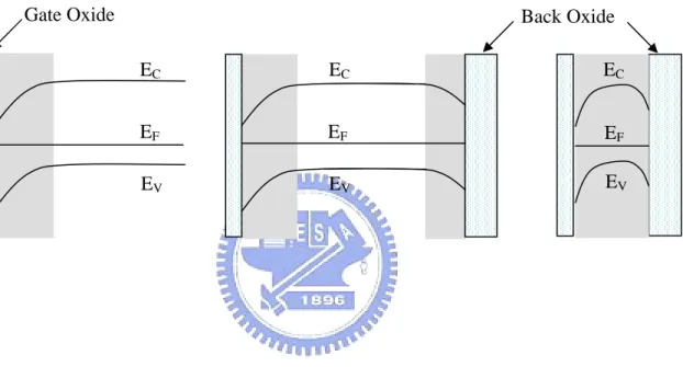
Fig.1-1 Band diagram in (a) bulk, (b) PD SOI, and (c) FD SOI. The shaded areas
represent the depleted region.
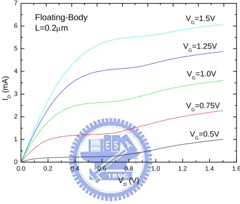
Fig.1-2 ID-VD characteristic of a PD floating-body SOI MOSFET at different gate biases
with L=0.2mm.
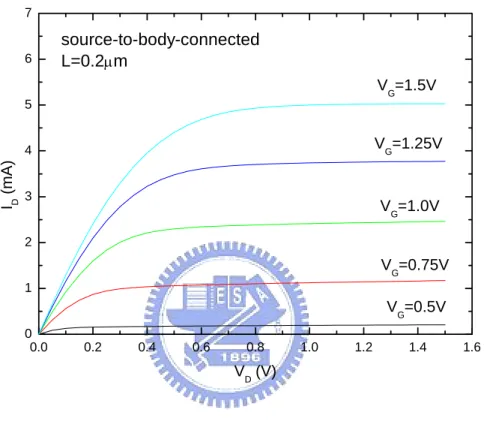
Fig.1-3 ID-VD characteristic of a PD source-to-body-connected SOI MOSFET at different
gate biases with L=0.2mm.
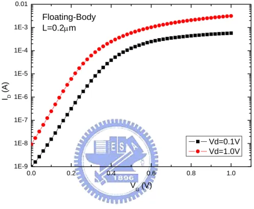
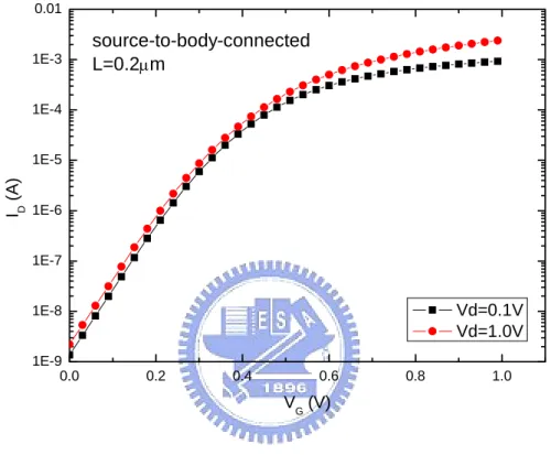
Fig.1-4 ID-VG characteristic of a PD floating-body SOI MOSFET at VD=0.1V and 1.0V
with L=0.2mm.
Fig.1-5 ID-VG characteristic of a PD source-to-body-connected SOI MOSFET at VD
=0.1V and 1.0V with L=0.2mm.
CHAPTER 2
Fig.2-1 Schematic plot of low frequency noise components Fig.2-2 Noise sources in a SOI MOSFET.
Fig.2-3 ID-VD curves in floating body SOI MOSFET
Fig.2-4 Noise small-signal equivalent circuits for the floating body SOI MOSFET
CHPATER 3
Fig.3-1 Input referred noise spectra of a PD floating body SOI MOSFET with different
drain biases.
Fig.3-2 Input-referred noise spectra of a PD floating-body SOI MOSFET at VDS = 1.0V
with different channel lengths.
Fig.3-3 Plateau and corner frequency of the input-referred noise for a PD floating-body
SOI MOSFET at VG-VT = 0.5V and VDS = 1.0V with different channel lengths.
Fig.3-4 Drain-body junction leakage current as functions of channel length for a PD
floating-body SOI MOSFET with different drain voltages.
Fig.3-5 Body capacitance as a function of channel length for a PD floating-body SOI
MOSFET at VG-VT = 0.5 V and VDS = 1.0V.
Fig.3-6 Input-referred noise spectra of a PD source-to-body-connected SOI MOSFET at
VDS = 0.1V and L=0.2mm with different VG-VT.
Fig.3-7 The magnitude of input-referred noise as a function of gate voltage for a PD source-to-body-connected SOI MOSFET at VDS = 0.1V, L=0.2mm and f=10Hz.
Fig.3-8 The magnitude of input-referred noise as a function of channel length for a PD
source-to-body-connected SOI MOSFET at VDS = 0.1V and f=10Hz.
CHAPTER 4
Fig.4-1 Input-referred noise spectra of a PD floating-body SOI MOSFET at VDS = 0.1V
with different temperatures.
Fig.4-2 Input-referred noise spectra of a PD floating-body SOI MOSFET at VDS = 0.8V
with different temperatures.
Fig.4-3 Plateau and corner frequency of the input-referred noise for a PD floating-body
SOI MOSFET at VG-VT = 0.4V and VDS = 0.8V with different temperatures.
Figure also shows the magnitude of the input-referred noise at f = 50Hz for a PD floating-body SOI MOSFET at VG-VT = 0.4V and VDS = 1.2V.
Fig.4-4 Drain-body junction leakage and body capacitance as functions of temperature
for a PD floating-body SOI MOSFET at VG-VT = 0.4V and VDS = 0.8V.
Fig.4-5 Leakage current versus 1/T for a PD floating-body SOI MOSFET at VG-VT =
0.4V and VDS = 0.8V.
Fig.4-6 Input-referred noise spectra of a PD floating-body SOI MOSFET at VDS = 1.2V
with different temperatures.
Fig.4-7 Input-referred noise spectra of a PD source-to-body-connected SOI MOSFET at
VDS = 0.1V with different temperatures.
Fig.4-8 Input-referred noise spectra of a PD source-to-body-connected SOI MOSFET at
VDS = 1.2V with different temperatures.
CHAPTER 5
Fig.5-1 Input-referred noise spectra of a PD floating-body SOI MOSFET at VDS = 0.1V
in normal and reverse mode before and after stress.
Fig.5-2 Input-referred noise spectra of a PD floating-body SOI MOSFET at VDS = 2V in
normal and reverse mode before and after stress.
Fig.5-3 Schematic diagrams of a MOSFET operated in (a) the normal mode and linear
region; (b) the reverse mode and linear region; (c) the normal mode and saturation region; and (d) reverse mode and saturation region. The position of the interface trap is indicated symbolically by the cross (µ)
Fig.5-4 Input-referred noise spectra of a PD floating-body SOI MOSFET at VDS = 1.2V
in normal and reverse mode before and after stress.
Fig.5-5 ID-VG characteristic of a PD floating-body SOI MOSFET in normal mode
before and after stress with W=20mm and L=0.5mm.
before and after stress with W=20mm and L=0.5mm.
Fig.5-7 Threshold voltage degradations as a function of stress time in floating-body and
body contact device.
Fig.5-8 Drain current degradations as a function of stress time in floating-body and
body contact device.
Fig.5-9 Input-referred noise spectra of a PD body contact SOI MOSFET at VDS = 0.1V
before and after stress.
Fig.5-10 Input-referred noise spectra of a PD body contact SOI MOSFET at VDS = 2V
Chapter 1
Introduction
1.1 Characteristic of Silicon-On-Insulator MOSFETs
1.1.1 Merit of SOI MOSFETs
Silicon-on-insulator (SOI) CMOS technology is currently considered a likely candidate for integrated digital and RF circuit applications, since it provides full dielectric isolation and reduced junction capacitance as compared to bulk-Si MOSFET. The substrate used in SOI technology includes silicon-on-sapphire, silicon-on-nitride, silicon-on-spinel, and silicon-on-oxide…etc., this insulator layer we discuss in this thesis is based on the oxide layer.
For SOI MOSFETs, the parasitic capacitances from drain to bulk and source to bulk are dominated by the buried oxide capacitance. Because the dielectric constant of buried oxide (εox=3.9) is smaller than that of silicon (εSi=11.9), the junction located on buried oxide gives
rise to a parasitic capacitance approximately three times smaller than that of a bulk junction. Therefore, the junction capacitances in SOI MOSFETs are smaller than those in bulk MOSFETs. As a result, the device has higher response speed and lower power consumption properties. Moreover, the isolation provided by the buried oxide has excellent immunity to against high energy particle illumination which results in the generation of electron-hole pairs and leads to a large amount of current. Hence, the leakage induced by radiation and the substrate junction of MOSFETs can be reduced. Besides, the thickness of the Si active layer can only be 50nm, which is good for producing ultra-shallow junctions to restrain the short channel effect. For SOI CMOS devices, because of the absence of the n-well and p-well, the
latch-up which caused by the parasitic npn and pnp BJTs in the well and the substrate will not happen. In addition, the isolation between devices can be performed by etching the Si film because of the thinner Si active layer only 50-200nm. Therefore, the SOI CMOS technology has a higher device density and a simple isolation process.
Although the buried oxide provides many advantages, it still leads to some drawbacks: self heating and floating body effect. The former is due to the low thermal conductivity of the buried oxide; hence it is less efficient to remove the excess heat than bulk MOSFETs. The later is because of a parasitic bipolar transistor in SOI MOSFETs. If we consider an n-channel device, the N+ source, the P-type body and the N+ drain indeed form the emitter, the base, and the collector of an NPN bipolar transistor. In a bulk device, the base of the bipolar transistor is usually grounded by means of a substrate contact. However, in an SOI device, the body (base) is usually left floating. Therefore, this parasitic bipolar transistor is the origin of several undesirable effects in SOI devices [1-3].
1.1.2 Partially Depleted and Fully Depleted SOI MOSFETs
According to the thickness of the silicon film, two types of devices can be distinguished: partially-depleted device (PD) and fully-depleted devices (FD), as shown in Fig. 1-1. If the silicon film is thick enough that the depletion region of the top portion and the bottom portion can not overlap, then there exists a piece of neutral region in the body. Such SOI MOSFETs is called PD device. On the contrary, if the silicon film is thin enough to let these two depletion regions overlap, this type of SOI MOSFETs is called FD device.
In PD SOI devices, because the depletion region is independent of the Si film thickness, the threshold voltage is insensitive to the film thickness and is the same as in a bulk transistor. However, the PD SOI devices will suffer floating body effect, which will be discussed in section 1.1.3, and create some undesirable phenomena. When the body is connected to ground, the floating body effect can be suppressed and the device is similar to bulk device. Moreover,
the suppression of the floating body effect with body contact can also reduce the kink-related excess noise in SOI MOSFETs at low frequency [4-5]. Although FD SOI MOSFETs have excellent performance compared with PD SOI devices, PD SOI technology is attractive for manufacturing because the substrate and source/drain doping engineering in bulk technology is applicable to PD devices, and the controllability over SOI film thickness is much better in PD SOI than in FD SOI technology.
In FD SOI devices, the produced one–dimensional character to the electric field line results in neutrally kink-free, if the back interface is not in accumulation. Generally speaking, the FD SOI devices have better DC properties, such as higher transconductance, smaller short channel effect, lower threshold voltage, and higher subthreshold swing, than the PD SOI devices. The larger gate control capability over the silicon film results in higher transconductance. And the smaller short channel effect which limits gate control of the channel in sub-micron devices is due to the one–dimensional field line. Besides, FD SOI devices are more suitable for the low power and low voltage applications according to reduced threshold voltage and parasitic capacitances. Owing to the thinner film in FD devices, shallower junctions could automatically be formed making reduced threshold voltage roll-off when devices shrink. However, owing to the relation of the depletion width and the Si film thickness, the threshold voltage is sensitive to the Si film thickness, and may vary with the process. Therefore the uniformity of SOI thickness also leads to the variation of threshold voltage from one device to another one or from this die to another die.
1.1.3 Floating-Body Effect
Owing to the buried oxide isolation, the charges caused by impact ionization store in the floating body, resulting in many undesirable phenomenons. These various phenomenons are generically referred to as floating-body effects.
enhancement-mode SOI MOSFETs operated in strong inversion, as shown in Fig. 1-2. As the drain voltage increases, the impact ionization occurs, which leads to the generation of the electron and hole pairs. The electrons flow into the drain, and the holes flow into the body. Owing to the existence of buried oxide, the holes stored in the floating body will raise the body potential and let the threshold voltage to be reduced. Thereby causing an excess drain current and producing many more electron-hole pairs through the avalanche process. This positive feedback results in a sudden increase in drain current or “kink” in ID-VD
characteristics. For source-to-body-connected PD device, the "kink" disappeared due to body contact (see Fig. 1-3). This suggests that the body contact can release the holes stored in the body and reduce the body potential.
The generation of majority carriers, holes, by impact ionization near the drain can give rise to an increase of body potential and decrease of the threshold voltage. Sometimes, a similar effect can occur at gate voltages lower than the threshold voltage. If the drain voltage is high enough, impact ionization can occur in the subthreshold region, even though the drain current is very small. When the gate voltage is increased, the weak inversion current can induce impact ionization in the high electric field region near the drain, resulting in the generation of the holes and the increase of the body potential. Therefore, the threshold voltage is reduced and the ID-VG curve shifts to the left, as shown in Fig. 1-4. For
source-to-body-connected PD device, the holes can be released by body contact and the deviation can be suppressed as shown in Fig. 1-5 [6].
1.2 Motivation
Recently, the rapid growth of the portable communication market requires the miniaturization of the whole system with as little power consumption as possible, leading to the trend of the integration of systems on a single chip. Therefore, SOI CMOS is a potential
candidate for integrated digital and RF applications due to its reduced junction capacitances, and good isolation which let SOI has some superior properties: high speed, low power consumption, higher device density [7-8]. However, as opposed to such optimistic condition, there are some hurdles to overcome. One of the technical problems is related to the floating operation of the partially-depleted devices, when the impact-ionization current near the drain is generated for the sufficiently large drain voltage, it gives rise to the well known kink in the drain current. Associated with the kink is a drastic increase of the low-frequency noise in devices for analog circuit application. The low-frequency noise can be up-converted in RF homodyne mixers and voltage-controlled-oscillators (VCOs), resulting in phase noise [9]. It places a fundamental limit on signal detection and spectral purity. For low-voltage analog circuit operation, low-frequency noise becomes even more important, because it needs tighter control on circuit performance. Hence, low-frequency noise is an important figure-of-merit for RF analog circuit. Therefore, to predict and develop approaches to suppress the amount of noise in SOI is a significant topic for study.
1.3 Organization of the Thesis
This thesis is divided into six chapters. In chapter 2, the theory of the low-frequency noise in PD SOI MOSFETs including 1/f noise and kink related excess noise will be described in detail. In chapter 3, the low-frequency noise in PD SOI MOSFETs with floating-body and source-to-body-connected structures were measured. The noise characteristics of the devices at different channel lengths were discussed. In chapter 4, we discussed the low-frequency noise in PD SOI MOSFETs operating from linear region to saturation region at various temperatures. In chapter 5, the degradation of low-frequency noise in PD SOI MOSFETs after hot-carrier stress was discussed. Finally, some conclusions about the measured results and future work were given in Chapter6.
EC EV EF EC EF EV Back Oxide Gate Oxide EV EF EC
Fig. 1-1 Band diagram in (a) bulk, (b) PD SOI, and (c) FD SOI. The shaded areas represent the depleted region.
0.0 0.2 0.4 0.6 0.8 1.0 1.2 1.4 1.6 0 1 2 3 4 5 6 7 Floating-Body L=0.2µm VG=1.5V V G=0.5V V G=0.75V VG=1.0V VG=1.25V I D (m A) V D (V)
Fig. 1-2 ID-VD characteristic of a PD floating-body SOI MOSFET at different gate
0.0 0.2 0.4 0.6 0.8 1.0 1.2 1.4 1.6 0 1 2 3 4 5 6 7 VG=0.5V VG=0.75V VG=1.0V VG=1.25V VG=1.5V source-to-body-connected L=0.2µm I D (m A) VD (V)
Fig. 1-3 ID-VD characteristic of a PD source-to-body-connected SOI MOSFET at
0.0 0.2 0.4 0.6 0.8 1.0 1E-9 1E-8 1E-7 1E-6 1E-5 1E-4 1E-3 0.01 Floating-Body L=0.2µm I D (A) VG (V) Vd=0.1V Vd=1.0V
Fig. 1-4 ID-VG characteristic of a PD floating-body SOI MOSFET at VD=0.1V and
0.0 0.2 0.4 0.6 0.8 1.0 1E-9 1E-8 1E-7 1E-6 1E-5 1E-4 1E-3 0.01 I D (A) VG (V) Vd=0.1V Vd=1.0V source-to-body-connected L=0.2µm
Fig. 1-5 ID-VG characteristic of a PD source-to-body-connected SOI MOSFET at
Chapter 2
Theory of Low-Frequency Noise in PD SOI MOSFETs
The low-frequency noise in PD SOI MOSFETs includes 1/f noise and kink related excess noise (also called Lorentzian-like noise overshoot) as shown in Fig. 2-1 where kink related excess noise superimposed on the 1/f noise. Among the total, 1/f noise is associated with the conductance fluctuation in channel and kink-related excess noise is associated with the body potential fluctuation due to floating-body effect.
2.1 1/f noise in PD SOI MOSFETs
The 1/f noise in PD SOI MOSFETs is common to all types of MOSFETs. The source of this noise comes from a fluctuation in the conductivity. There are two competing models appeared in the literature to explain it: the McWhorter carrier number fluctuation theory and the Hooge mobility fluctuation theory. There is experimental evidence to support both theories, and thus the literature is mostly split into two camps over the issue.
The number fluctuation theory is attributed to random trapping and detrapping processes of charges in the oxide traps near the Si-SiO2 interface, i.e. the channel can exchange charges
with the oxide traps through tunneling. Besides, this model is based on the concept of generation recombination noise and such kind of noise usually occurs at the interface or junction of semiconductors. Therefore, number fluctuation theory is a surface effect. The traditionally derived result of the number fluctuation model for uniform trap distribution is:
( )
2 2 2 ( ) 8 t fn VG ox N E kTq V S Hz WLC α f = ⋅ (2-1)* 2 1/ 2
(2me B/ )
α = φ =
2
1/WLCox
where is typically taken to equal 108cm-1, Nt(Efn) is the oxide trap density
adjacent to the electron quasi-Fermi level in silicon, and f is the frequency in Hertz. From equation (2-1), the gate voltage noise power spectral density is independence of the gate voltage and proportional to [10].
(VGS −VT) /(WLCox)
The mobility fluctuation theory, based on Hooge’s relation, is an empirical model able to fit noise data in homogeneous semiconductors and devices. Hooge considers the 1/f noise as a result of the fluctuation in bulk mobility and is no surface effect. When Hooge’s relation is directly applied to MOSFET’s, it predicts an equivalent gate voltage noise power spectral density which is proportional to [11].
Except the model we discuss above, some people proposed the theory combining with number and mobility fluctuation to be the third method. And it becomes the popular one. In such models, the number fluctuation term is independence of gate bias; and the mobility fluctuation term is proportional to the square of gate drive voltage [10], [12].
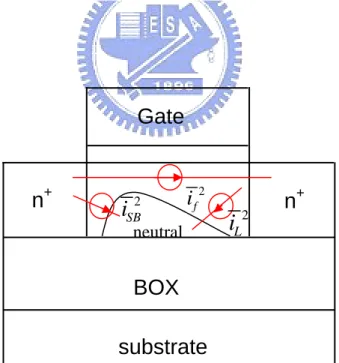
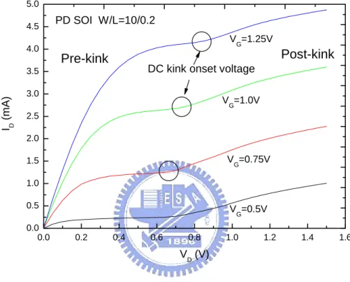
2.2 Kink related excess noise in PD SOI MOSFETs
Due to the floating body, SOI MOSFETs exhibit a low frequency kink-related noise overshoot, which has a Lorentzian spectrum: a flat low-frequency plateau, with constant amplitude, followed by a 1/f2 roll-off. Therefore, the kink-related excess noise is also called
Lorentzian-like noise. Several mechanisms have been proposed to explain this excess noise, such as trap-assisted generation- recombination (G-R) noise caused by the defects in body region [13], G-R noise induced by back interface state caused by the defects at bottom Si-SiO2 interface [14], and shot noise amplified by the floating body effect [15]. In early years,
owing to the worse process, the G-R noise is the main source of the excess noise. At present, the technology of the process is quite advanced, thus the defects in Si film and bottom Si-SiO2
become the major sources. The shot noise sources from drain to body and source to body result from the drain-body junction leakage (IL) and body-source diode current (ISB)
respectively (see Fig. 2-2). Although both are shot noises generated by flow of carriers surmounting energy barriers, they are independent noise sources. However, these two noises are basically the same, because in SOI IL is roughly equal to ISB as a result of current
balancing in the body of SOI device. Here we defined the region, which the drain biasis smaller than the dc kink onset voltage, as “pre-kink region”. On the contrary, when the drain biasis larger than the dc kink onset voltage, the region is defined as “post-kink region” (see Fig. 2-3). In the pre-kink region, where the drain voltage is small, impact ionization can be neglected; therefore IL is dominated by junction thermal generation current (IG). In the
post-kink region, where the drain voltage is large enough to lead to impact ionization, the IL is
dominated by impact ionization current (Iii).
The shot noise originates in the IL and ISB are small in magnitude compared with flicker
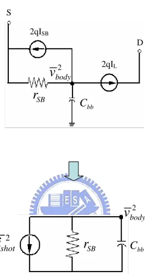
noise, but the high impedance of source-body junction caused by floating body effect significantly amplifies their magnitude and gives rise to the excess low-frequency noise in PD SOI MOSFET. From the shot noise model proposed by Jin [16], the shot noises can be express as (2qISB+2qIL) which are a white noise. The source-body junction impedance (Zbody)
is the parallel combination of rSB and CBB. These current fluctuations perturb the body voltage
through the square of the body impedance with Lorentzian-like shape similar to a RC filter shown in Fig 2-4, and no longer be a white noise [17]. After that, these body voltage fluctuations transferred through the body effect to gate voltage power spectral density (V2/Hz),
as followed:
(
)
2 2 2 2 2 , 2 2 2 2 2 2 0 0 | | (2 2 ) 1 2 1 1 4( ) 1 4 ( ) 1 1 TH SBVG excess shot Body SB L
BS S L B BB T L V r S i Z qI qI V f r C nkT q nV qI f f f f I α π α α ⎛∂ ⎞ = × ×⎜ ⎟ = + × ⋅ ∂ + ⋅ ⎝ ⎠ = ⋅ ⋅ ⋅ = ⋅ ⎛ ⎞ ⎛ ⎞ +⎜ ⎟ +⎜ ⎟ ⎝ ⎠ ⎝ ⎠ (2-2)
source-body junction resistance, CBB is the body-ground capacitance, and f0 =qIL /(2π nkTCBB
). Therefore, the corner frequency f0 is proportional to IL and the plateau is proportional to 1/ IL.
As the operation mode shifts from PD toward more FD operation, source-body junction diode saturation current, IR (where source-body junction diode current ISB=IR⋅(exp(VSB/nVT)-1))
exponentially increases due to the reduced source-body junction barrier, as follows:
(2-3)
/
( ) ( ) qVBS kT
R R
I FD =I PD ×e ′
where V'BS is the reduced junction barrier potential. Exponential increase of IR in FD SOI
devices results in a significant decrease of source-body junction impedance Zbody (i.e. shot
noise amplified gain). Therefore, the floating body effect is suppressed by an increase of IR,
and IR has to be included in the excess noise model with a modification of r'SB=nVT/(ISB+IR) as
(
)
2 2 , 2 2 2 2 0 2 (2 2 ) 1 2 1 ) 4 ( ) ( 1 SB VG excess SB L SB B T L L B R r S qI qI f r C q nV I f I I f α π α ′ = + × ⋅ ′ + ⋅ = ⋅ ⋅ ⋅ + ⎛ ⎞ + ⎜⎝ ′⎟⎠ (2-4)where f'0=1/(2π r'SBCBB) and is proportional to IL+IR. According to equation (2-3), as the
operation toward more FD, IR will increase and thus lead to the increase of f'0 and reduction of
the plateau. If the magnitude of plateau is smaller than 1/f noise, then we can observe only 1/f noise, i.e. the shot noise is suppressed.
The other way to reduce excess noise is using body contact. A good body contact provides another low-resistance discharge path for body charges, and the impedance of current fluctuation can drastically reduce (i.e. shot noise amplified gain can reduce), as follows:
B body body
where RB is the body path resistance. The criterion for low frequency noise optimization is to
suppress the Lorentzian-like noise overshoot making it less than the underlying 1/f noise by decreasing the body transfer function at the desired biases.
1/f 2 plateau
Flicker noise
∝
1/ f
21
Lorentzian spectrum
1 ( /
f
f
o)
∝
+
SVG (V 2 /Hz) f0 Frequency (Hz)substrate
n
+Gate
n
+ neutral 2 fi
2 SBi
2 Li
Fig. 2-1 Schematic plot of low frequency noise components
BOX
Fig. 2-2 Noise sources in a SOI MOSFET.
:1/f noise : shot noise due to body-source diode current: shot noise due to drain-body junction leakage 2 f
i
2i
S B 2 Li
0.0 0.2 0.4 0.6 0.8 1.0 1.2 1.4 1.6 0.0 0.5 1.0 1.5 2.0 2.5 3.0 3.5 4.0 4.5 5.0 V G=1.25V V G=0.5V V G=0.75V V G=1.0V Post-kink I D (mA) VD (V)
DC kink onset voltage Pre-kink
PD SOI W/L=10/0.2
S 2 body
v
SBr
bbC
2qIL 2qISB D 2 shoti
C
bb 2 bodyv
SBr
Fig. 2-4 Noise small-signal equivalent circuits for the
floating body SOI MOSFET
Chapter 3
Characterization of Low-Frequency Noise
in PD SOI MOSFETs
In this chapter, we describe the measurement methods for I-V and low-frequency noise characterization firstly. Then we discuss the noise characteristics of PD SOI MOSFETs with floating-body and source-to-body-connected structures. Because of the continuous scaling-down of devices for better performance, it is important to realize and model the low-frequency noise in SOI MOSFETs after channel shrinking for device process diagnosis and analog circuit simulation. Hence the influence of channel length on the low-frequency noise of PD SOI MOSFETs also has been investigated in this chapter.
3.1 Devices under Test and Measurement Techniques
3.1.1 Devices under Test
The n-channel MOSFETs were fabricated on Separation by Implantation of Oxygen (SIMOX) substrates with 190nm thick Si active layers, 150nm thick buried oxides, and 1.6nm nitride gate oxides. The floating-body and source-to-body-connected transistors with oxide/SiN spacers and As+-implanted source/drain junctions are partially depleted. After CoSi2 salicidation, the devices were metalized using a typical backend flow.
3.1.2 I-V Measurement
From the ID-VG curves, we extract the threshold voltage (VTH), transconductance (gm=dID /dVG ) and body factor (α=dVTH /dVBS ) at different channel lengths. We also observed the
kink effect from the ID-VG and ID-VD characteristics.
3.1.3 Noise Measurement
The HP4145, HP35670A Dynamic Signal Analyzer, and BTA9812 Noise Analyzer were employed to measure the low frequency noise at different channel lengths, where the measurement system was fully automated using a personal computer via HP-IB. The measurement frequency range is from 1Hz to 10 kHz, and the output drain current noise power spectrum would be extracted. We divide the output drain current noise power spectrum by the square of the transconductance to obtain the input-referred gate voltage noise power spectrum (i.e. SVG=SID /gm2).
The devices operate in linear operation are corresponding to a drain voltage VDS = 0.1V.
As the drain bias increases to about 0.4V, the devices enter the saturation region, both the data obtained before the kink occurring (VDS = 0.8V) and after the kink occurring (VDS = 1.0V) are
shown.
3.2 Low-Frequency Noise in Floating-Body Devices
3.2.1 Low-Frequency Noise at Various Drain Voltages
The low-frequency noise characteristics of a floating-body PD SOI MOSFET at room temperature are shown in Fig. 3-1. Measured noise spectra exist a Lorentzian-like noise overshoot superimposed on the pure 1/f noise. The Lorentzian-like noise overshoot has a plateau followed by a 1/f 2 roll-off at the corner frequency f0, where the noise is 3 dB under the
floating-body effect. The plateau and corner frequency show a strong dependence on the drain bias. When the device operates at high drain bias, the 1/f noise, whose magnitude is inversely proportional to the frequency f, is visible at low frequency. It has been reported that the origin of 1/f noise is the carrier number fluctuation and the mobility fluctuation, which lead to the 1/f noise in MOSFETs.
The equation of the input-referred gate voltage noise proposed by Tseng [15] which we described in Chapter 2 is:
(
)
2 , 2 0 4( ) 1 1 / VG excess L nkT S qI f f α = ⋅ + (3-1)where kT is the thermal energy, n is the junction ideality factor, q is the elementary charge,
α (=dVTH/dVBS) is the body factor, and IL is the drain-body junction leakage. The corner
frequency of the Lorentzian spectrum is given by f0 = qIL / (2πnkTCbb), where Cbb is the
capacitance associated to the body. Therefore the plateau is proportional to 1/IL, and f0 is
proportional to IL. The increase of drain bias should increase the junction leakage current IL,
and thus lead to the increase of f0 and the reduction of the plateau. As the drain bias increases
to 1.2V, the impact ionization current will get higher too, and the IL will increase significantly,
so the noise overshoot will be suppressed below the 1/f noise in low frequency range.
3.2.2 Low-Frequency Noise at Various Channel Lengths
Fig. 3-2 shows the low-frequency noise characteristics of a floating-body PD SOI MOSFET operating at VDS=1.0V, where the Lorentzian-like noise overshoot was observed
explicitly at various channel lengths. When the channel length increases, the plateau increased and the corner frequency f0 decreased [18]. Since the noise magnitude is related to the IL, α,
in Fig. 3-3 by using equation (3-1). By analyzing the IL, α, and Cbb at different channel
lengths, the relation between noise magnitude and channel length can be obtained. For our device under test, the body factor α is nearly independent on channel length and drain bias, and its value is about 0.22. However, the IL and Cbb are strong functions of channel length, as
shown in Fig. 3-4 and Fig. 3-5. When VDS=1.0 V, IL is dominated by impact ionization current
because the drain bias we gave exceeds the kink onset voltage. The substrate leakage current due to impact ionization can be expressed as:
sub DS i
I =I ⋅ ⋅ ∆α L (3-2)
where αi is the ionization coefficient, the number of electron-hole pairs generated per unit
distance; and DL is the length of the pinch-off region. As the channel length increases, the lateral field ((VD-VDsat)/L) decreases, causing a reduction of αi. Besides the IDS also decreases
as the channel length increases. Therefore, the IL is proportional to 1/Lγ , where g is affected
by the total influence of IDS and αi, as shown in Fig.3-4. As the drain voltage reduces, and the
device operates in the pre-kink region (VDS=0.8 V), the extracted value of IL is nearly
independent on channel length as opposed to that at VDS=1.0 V (see Fig. 3-4). It is because the IL is dominated by the thermal generation current in pre-kink region and can be expressed as:
2 p i i R p D e D n qn W J q N τ τ = + (3-3)
Therefore, the IL is independent on channel length. In Fig. 3-5, the Cbb increases
monotonously with increasing the channel length. As the channel length increases, the capacitances from body to gate and body to substrate increase due to the increasing of channel area. However, the capacitances from body to source and body to drain are independent on channel length. Therefore, the slope of Cbb curve is less than unity.
3.3 Low-Frequency Noise in Body-to-Source-Connected Devices
The input noise spectrum of a body-to-source-connected PD device is shown in Fig. 3-6, where the channel length is 0.2 mm, and VDS=0.1 V. We observed that the noise spectrum is
dominated by 1/f noise. This suggests that the source-to-body connection can suppress the noise overshoot efficiently. This is because the body contact provides a low-resistance discharge path for body charges, where the source-body impedance reduces drastically by the parallel combination of RB and Zbody. The RB is the body path resistance and Zbody
(=rSB/(1+j(2πf⋅rSBCBB))) is the source-body impedance [19]. Once the source-body impedance
reduces by body contact, the shot noise amplified gain would be reduced. Therefore, only 1/f noise would be observed in source-to-body-connected devices.
In MOSFETs, the 1/f noise magnitude is usually related to the interface trap density between the silicon film and the gate oxide. A model, proposed by Gross [20], demonstrated that the noise in MOSFET is due to the fluctuation of the carrier number in the channel and that these fluctuations induce local correlated fluctuations in the channel mobility. When the device operates in linear region and a uniform distribution of oxide/silicon interface traps in activation energy is assumed, the input-referred voltage noise can be written as [20]:
2 2 0 2 0 2 4 ( ) ( ) (1 ) T f VG ox q x kT N E S fWLC
µ
≅ + SN (3-4), where W, L, Cox, µ0, and Sare the gate width, gate length, gate oxide capacitance, channel
mobility, and scattering parameter, respectively. NT (Ef) is the trap number near Fermi energy Ef, and the traps lie in the oxide distributed over some region x0 near the interface. Nis the
channel carrier number and is proportional to the gate drive voltage. From the equation (3-4), it is clear that the 1/f noise can stem from processing-induced variations in either the near-interface trap density NT, or in the scattering parameter S, for fixed operation conditions
and device area. If the induced mobility fluctuation term µ0SN <<1, the induced mobility
fluctuation can be neglected, and the noise power spectrum is independence of the gate drive voltage. On the contrary, if the term µ0SN >>1, the noise magnitude is proportional to the
square of gate drive voltage as shown in the Fig. 3-7. Hence, the 1/f noise component is dominated by induced mobility fluctuation. Fig. 3-8 shows the input noise spectrum versus channel length for a device operating at VDS=0.1 V. As shown in Fig. 3-8, the input noise
10 100 1000 10000 1E-15 1E-14 1E-13 1E-12 1E-11 1E-10 1E-9
f
01/f
1/f
2 excess noise S VG (V 2 /H z) Frequency (Hz) VDS=0.1V VDS=0.4V VDS=0.7V VDS=1.0V VDS=1.2V VG-VT=0.4VFig. 3-1
Input referred noise spectra of a PD floating body SOI MOSFET with different drain biases.10 100 1000 10000 1E-15 1E-14 1E-13 1E-12 1E-11 1E-10 1E-9 VDS=1.0V VG-VT=0.5V S VG (V 2 /H z) Frequency (Hz) L=0.12 L=0.2 L=0.3 L=0.45 1/f 2
Fig. 3-2
Input-referred noise spectra of a PD floating-body SOI MOSFET at VDS = 1.0V with different channel lengths.0.10 0.15 0.20 0.25 0.30 0.35 0.40 0.45 0.50 1E-13 1E-12 1E-11 1E-10 101 102 103 104 105 V DS=1.0V VG-VT=0.5V Coner F requency (Hz) S VG (V 2 /H z) Channel Length L (µm) plateau corner frequency
Fig. 3-3
Plateau and corner frequency of the input-referred noise for a PD floating-body SOI MOSFET at VG-VT = 0.5V and VDS = 1.0V0.10 0.15 0.20 0.25 0.30 0.35 0.40 0.45 0 5 10 15 20 25 V G-VT=0.5V Lea kage Curre n t I L (pA)
Channel Length L (um)
V
DS=1.0V
V
DS=0.8V
Fig. 3-4
Drain-body junction leakage current as functions of channel length for a PD floating-body SOI MOSFET with different drain voltages.0.10 0.15 0.20 0.25 0.30 0.35 0.40 0.45 0.50 0 2 4 6 8 10 12 VDS=1.0V VG-VT=0.5V Body Capacit ance C bb (fF)
Channel Length L (um)
Fig. 3-5
Body capacitance as a function of channel length for a PD floating-body SOI MOSFET at VG-VT = 0.5 V and VDS = 1.0V.10 100 1000 10000 1E-15 1E-14 1E-13 1E-12 1E-11 1E-10 1E-9 source-to-body-connected L=0.2µm VDS=0.1V S VG (V 2 /H z ) Frequency (Hz) Vg-Vt=0.1V Vg-Vt=0.3V Vg-Vt=0.5V Vg-Vt=0.7V Vg-Vt=1.1V 1/f
Fig. 3-6
Input-referred noise spectra of a PDsource-to-body-connected SOI MOSFET at VDS = 0.1V and L=0.2mm
0.1 1 1E-13 1E-12 1E-11 1E-10 1E-9 S VG (V 2 /H z) VG-VT (V) source-to-body-connected L=0.2µm f=10Hz V DS=0.1V
Fig. 3-7
The magnitude of input-referred noise as a function of gate voltage for a PD source-to-body-connected SOI MOSFET at VDS =0.1 1 10 1E-13 1E-12 1E-11 1E-10 1E-9 source-to-body-connected V DS=0.1V f=10Hz V G-VT=0.7 S VG (V 2 /Hz) Channel Length L (µm)
Fig. 3-8
The magnitude of input-referred noise as a function of channel length for a PD source-to-body-connected SOI MOSFET at VDS = 0.1V and f=10Hz.Chapter 4
Low-Frequency Noise in PD SOI MOSFETs at Various
Temperatures
Because the SOI MOSFETs have higher thermal resistance, the channel temperature is higher than bulk devices with the same power dissipation. In addition, there is increasing demand for high-temperature electronics with CMOS technology. The temperature characteristics of SOI devices on analog applications should be studied [21], [22]. In this chapter, we use Temptronic TP03000 Thermal Controller to vary the temperature and investigate the influence on the low-frequency noise of PD SOI MOSFETs operating from linear region to saturation region. The noise characteristics of the devices with floating-body and source-to-body-connected structures have been discussed. The gate length and gate width of test devices are 0.2µm and 10µm, respectively.
The devices operate in linear operation are corresponding to a drain voltage VDS = 0.1V.
As the drain bias increases to about 0.4V, the devices enter the saturation region, both the data obtained before the kink occurring (VDS = 0.8V) and after the kink occurring (VDS = 1.2V) are
shown.
4.1 Temperature Effect on Floating-Body PD Device
4.1.1 Operating in Linear Region
The low-frequency noise characteristics of a floating-body PD SOI MOSFET operating
in the linear region (drain voltage VDS = 0.1V) is given in Fig. 4-1. At T = 0oC, owing to such
ionization current have very low values, resulting in a higher plateau and lower f0. Therefore,
the noise overshoot only exists in low frequency range (f < 100Hz), and the 1/f noise dominates. As the temperature increases, the intrinsic carrier density (ni ∝ T1.5⋅exp(-1/T ))
significantly increases, resulting in a larger junction thermal generation current. This large junction generation current contributes to a lower plateau and higher f0, thus the
Lorentzian-like noise overshoot begins moving to higher frequency and exceeds the 1/f noise gradually, as shown in Fig. 4-1. With further increasing temperature to T = 150oC, the noise overshoot shifts to lower plateau and higher corner frequency due to the increase of junction generation current and a Lorentzian-like noise overshoot was observed explicitly.
4.1.2 Operating in Saturation Region and Pre-kink Region
A similar phenomenon is observed in Fig. 4-2 for a floating-body device operating in saturation region before kink effect occurring (The kink voltage is about 0.9V), but an obvious noise overshoot has already appeared at T = 0oC due to the higher junction generation current than that in linear region. Since the junction leakage increases more rapidly at higher temperature, the magnitude of noise overshoot would be decreased drastically with the rise of temperature, as shown in Fig. 4-3.
To further see the effect of the IL, α, and Cbb on the temperature behavior of the noise
overshoot, we extract their values from the plateau and corner frequency of noise overshoot in Fig. 4-3 by using equation (3-1). We find that the body factor is nearly independent on temperature and drain bias, and its value is about 0.22. However, the IL and Cbb are strong
functions of temperature, as shown in Fig. 4-4. As the temperature increases, intrinsic carrier density increases, resulting in the decreasing of the depletion width, and therefore the Cbb
increases monotonously. The exponential function of IL with temperature indicates the
shown in Fig.4-5, the activation energy Ea for junction leakage can be extracted: Ea = 0.21eV
at low temperature (T ≤ 750C), and Ea = 0.42eV at high temperature. The equation of the
junction leakage including ideal and nonideal cases can be expressed as:
2 p i i R p D e D n qn W J q N τ τ = + (4-2)
The first term is the diffusion current, while the second term is the generation current due to the generation-recombination processes through the traps in the depletion region. If the junction leakage is dominated by the first term, owing to JR1 ∝ ni2 ∝ exp(-Eg/kT) (where
bandgap energy Eg=1.1 eV), the value of Ea is approximately 1.1 eV. If the second term
dominates, owing to the equation JR2 ∝ ni ∝ exp(-Eg/2kT), the value of Ea is approximately
0.55 eV. Since the extracted Ea in our devices is smaller than 0.55 eV, it suggests that the
thermal generation current is trap dominated in the temperature range of 0-1500C [23].
4.1.3 Operating in Saturation Region and Post-kink Region
As the device operates in the post-kink region (VDS=1.2 V), the large junction leakage
current makes the noise overshoot only exists in higher frequency (f > 1 kHz) and is approximately constant up to 75oC, as shown in Fig. 4-6. This is because the impact-ionization current generated near the drain overwhelms the thermal generation current and dominates the leakage current, and the impact-ionization current is less sensitive to temperature as compared to junction generation current [24]. Above 150oC, the drain to body junction generation current drastically increases and dominates leakage current, resulting in a lower plateau than the other temperature conditions. Except for the higher frequency, a pure 1/f noise has been observed over the range of measurement temperature. In addition, we find that the 1/f noise component is temperature-independent.
4.2 Temperature Effect on Body-to-Source-Connected PD Device
We may compare the noise measurements of floating-body SOI transistors with those of source-to-body-connected devices. As shown in Figs. 4-7 and 4-8, the input noise spectrum is dominated with 1/f noise component, and may contain small Lorentzian-like noise for some devices. This suggests that the noise overshoot can be suppressed by body contact. It is noted that the 1/f noise is independent of temperature as the case of floating-body device at high drain bias. From section 3.3 we know that the 1/f noise in SOI devices is dominated by induced mobility fluctuation, and the induced mobility fluctuation term µ0SN has a large
effect on the variation of 1/f noise with temperature, yielding a relatively temperature-independent characteristic shown in Fig.4-7 and 4-8. We compare Figs. 4-6 and 4-8, the magnitudes of 1/f noise in floating-body devices and source-to-body-connected devices have approximate values. It suggests that the two types of devices have similar trap density. Therefore, the body contact structure wouldn’t affect the gate oxide quality [25].
10 100 1000 10000 1E-15 1E-14 1E-13 1E-12 1E-11 1E-10 1E-9 W/L=10/0.2 µm S VG (V 2 /H z ) Frequency (Hz) T=0OC T=25OC T=75OC T=150OC VDS=0.1V V G-VT=0.4V 1/f 1/f2
Fig. 4-1
Input-referred noise spectra of a PD floating-body SOI MOSFET at VDS = 0.1V with different temperatures.10 100 1000 10000 1E-15 1E-14 1E-13 1E-12 1E-11 1E-10 1E-9 W/L=10/0.2 µm S VG (V 2 /H z) Frequency (Hz) T=0OC T=25OC T=75OC T=150OC VDS=0.8V VG-VT=0.4V
1/f
2Fig. 4-2
Input-referred noise spectra of a PD floating-body SOI MOSFET at VDS = 0.8V with different temperatures.-20 0 20 40 60 80 100 120 140 160 1E-12 1E-11 1E-10 1E-9 101 102 103 104 105 SVG@ f=50Hz corner frequency Co ner F req uen cy (Hz) S VG (V 2 /H z) Temperature (0C) VDS=0.8V VDS=1.2V Floating-Body VG-VT=0.4V plateau
Fig. 4-3
Plateau and corner frequency of the input-referred noise for a PD floating-body SOI MOSFET at VG-VT = 0.4V and VDS = 0.8Vwith different temperatures. Figure also shows the magnitude of the input-referred noise at f = 50Hz for a PD floating-body SOI MOSFET at VG-VT = 0.4V and VDS = 1.2V.
-20 0 20 40 60 80 100 120 140 160 -1 0 1 2 3 4 5 6 1 2 3 4 5 6 7 8 9 Body Capac it anc e C bb (fF) Lea kage Current I L (p A) Temperature (oC)
V
DS=0.8V
V
G-V
T=0.4V
Fig. 4-4
Drain-body junction leakage and body capacitance as functions of temperature for a PD floating-body SOI MOSFET at VG-VT = 0.4V and VDS = 0.8V.0.0022 0.0024 0.0026 0.0028 0.0030 0.0032 0.0034 0.0036 0.0038 1E-15 1E-14 1E-13 1E-12 1E-11 1E-10
V
DS=0.8V
V
G-V
T=0.4V
E a=0.42eV Le ak ag e Curre n t (A ) 1/T (K-1) Ea=0.21eVFig. 4-5
Leakage current versus 1/T for a PD floating-body SOI MOSFET at VG-VT = 0.4V and VDS = 0.8V.10 100 1000 10000 1E-15 1E-14 1E-13 1E-12 1E-11 1E-10 1E-9 W/L=10/0.2 µm S VG (V 2 /H z ) Frequency (Hz) T=0OC T=25OC T=75OC T=150OC
1/f
V
DS=1.2V
V
G-V
T=0.4V
Fig. 4-6
Input-referred noise spectra of a PD floating-body SOI MOSFET at VDS = 1.2V with different temperatures.10 100 1000 10000 1E-15 1E-14 1E-13 1E-12 1E-11 1E-10 1E-9 W/L=10/0.2 µm S VG (V 2 /Hz) Frequency (Hz) T=25OC T=75OC T=150OC source-to-body-connected V DS=0.1V V G-VT=0.4V 1/f
Fig. 4-7
Input-referred noise spectra of a PDsource-to-body-connected SOI MOSFET at VDS= 0.1V with different
10 100 1000 10000 1E-15 1E-14 1E-13 1E-12 1E-11 1E-10 1E-9 W/L=10/0.2 µm source-to-body-connected VDS=1.2V VG-VT=0.4V S VG (V 2 /H z) Frequency (Hz) T=25oC T=75oC T=150oC
Fig. 4-8
Input-referred noise spectra of a PDsource-to-body-connected SOI MOSFET at VDS= 1.2V with different
Chapter 5
Degradation of Low-Frequency Noise in PD SOI MOSFETs
after Hot-Carrier Stress
With the reduction of device size to deep submicrometer dimensions, the problem of the quality of the gate oxide and its interface with the silicon substrate due to hot-carrier effect has been of increasing concern in the fabrication of SOI CMOS devices. Because the 1/f noise is sensitive to oxide charge and interface traps, it is good to monitor the device reliability by measuring the 1/f noise. In this chapter, we investigate the influence of hot-carrier stress on the low-frequency noise of PD SOI MOSFETs including 1/f noise and shot noise induced kink-related excess noise. The noise characteristics of the devices with floating-body and body-contact structures have been discussed.
5.1 Experiments
The n-channel MOSFETs were fabricated on SIMOX substrates with 205nm thick Si active layers, and 400nm thick buried oxides. Briefly, 450nm LOCOS field oxide was used for device isolation. After VT-adjust implant and anti-punch through implant, a 4nm gate
oxide and in-situ n+-doped polysilicon gate were formed. The floating-body and body-contact devices with nitride spacer and As+-implanted source/drain junctions are partially depleted. After NiSi salicidation, the devices were metalized using a typical backend flow.
The current-voltage characteristics of devices were measured using HP4156A semiconductor parameter analyzer. The low-frequency noise measurements in normal and
reverse (i.e., source and drain interchanged) modes were performed using a BTA9812B noise analyzer in conjunction with an HP35670A dynamic signal analyzer. The hot-carrier stress was applied at a drain voltage of VDS = 4V and a gate voltage of VG = 2V with a stressing time
ranging from 0 to 1000 sec.
5.2 Hot-Carrier Effect on Floating-Body PD Device
Fig. 5-1 shows the low-frequency noise characteristics of a floating-body PD SOI
MOSFET operating in the linear region (VDS = 0.1V) before and after hot-carrier stress for
1000 seconds. The gate length and gate width of test devices are 0.4µm and 20µm, respectively. Owing to the low drain bias, the drain-body junction leakage is low, and the kink related excess noise was overwhelmed by the 1/f noise. After stress, there are two types of damages would affect the 1/f noise: interface states and oxide-trapped charge. In a stressed device, the energy transferred from the hot carriers to the Si/SiO2 interface would break the
bond at the interface and thus leads to the creation of the interface state. In n-MOS devices, only acceptor states which become negatively charged would cause an influence on it. When a charge is injected into the oxide after hot carrier stress, it can create a trap; and they are charged positively or negatively depending on this trap [26]. After stressing the device with 1000 seconds, the interface trap and oxide charge stem from hot carrier effect would be increased. From the model in chapter 2, the 1/f noise is proportional to the trap density Nt near
the Fermi-level.
(5-1)
VG t
S ∝N
Therefore, the 1/f noise would be increased after hot-carrier stress, and the similar phenomenon can also be observed in reverse mode. It is noted that, the magnitude of 1/f noise in the normal mode and the reverse mode have approximate values. However, in saturation condition (VDS = 2V), the magnitude of 1/f noise in the reverse mode is higher than that in the
normal mode, as shown in Fig. 5-2. Fig. 5-3 shows the hot-carrier degradation modes of a MOSFET operated in the linear and saturation regimes. In linear region, the effects of the trap are the same in both modes, nevertheless, in saturation region, the effect of the trap decreases in normal mode as the pinch-off region increases. For reverse mode operation, hot-carrier-induced interface traps are located on the source side, so the effect of the trap remains unchanged in saturation region [27], [28]. Therefore, the magnitude of the 1/f noise increased by hot-carrier stress in reverse mode is higher than that in normal mode.
Fig. 5-4 shows the low-frequency noise characteristics of a device operating in the saturation region and before kink effect occurring (VDS =1.2V). A Lorentzian-like noise
overshoot was observed explicitly before and after stress in normal mode. The noise overshoot comes from the interactionbetween the shot noise of the junction leakage and the source-body impedance, as illustrated in chapter 3. After stressing the device, the increased interface-trap density near the drain junction causes the increase of gate-induced-drain-leakage (GIDL) current in the low field region as shown in Fig. 5-5, and provides an additional current path due to the interface-trap assisted band-to-band tunneling mechanism; therefore, the trap-assisted drain-to-substrate leakage increases [29]. As discussed in chapter 3, when the drain-to-substrate leakage increases, the plateau of the kink-related excess noise will decrease, and the corner frequency will increase as shown in Fig. 5-4. In reverse mode, because the interface traps are located on the source side, the GIDL current would not be changed as shown in Fig. 5-6. Hence, the drain-to-substrate leakage would not be affected by stress and remain constant. However, the excess holes in body region due to the floating-body effect can effectively recombine through the interface traps near source with excess electrons due to the parasitic bipolar action. As a result, the floating-body effect is suppressed, thus the kink-related excess noise is suppressed. From Fig. 5-4, we only observe the 1/f noise after stress with reverse mode.
5.3 Hot-Carrier Effect on Body-Contact PD Device
To reduce floating body effect, the body contact structure is widely used in SOI CMOS technology. Hence we are also interested to know the hot-carrier effect on the performance of body-contact devices. Figs. 5-7 and 5-8 show the threshold voltage and drain current degradation respectively as a function of stress time in floating-body and body-contact devices. The gate length and gate width of test devices are 0.4µm and 20µm, respectively. It is noted that the degradation in body-contact device was larger than that in floating-body device. As the body voltage changes from high (floating-body device) to low (body-contact device), the vertical channel field increases, which means the channel electrons are pushed further toward the Si surface [30]. These hot channel electrons which closer to the Si surface would lead to greater Si surface damage. Therefore, the degradation which stems from hot-carrier stress was more serious in body-contact device. Figs. 5-9 and 5-10 show the low-frequency noise characteristics of a body-contact PD device operating in the linear and saturation region respectively. Because the body contact provides a low resistance leakage path, the shot noise amplified gain decreases, and the input noise spectrum is dominated with 1/f noise component. As the same with the floating–body devices, the 1/f noise would increase after hot-carrier stress due to the generation of the interface states and oxide charge.
10 100 1000 10000 1E-15 1E-14 1E-13 1E-12 1E-11 1E-10 1E-9 VD=0.1V VG=1.56V S VG (V 2 /H z) Frequency (Hz) t=0sec N t=1000sec R t=1000sec W/L=20µm/0.4µm 1/f
Fig. 5-1
Input-referred noise spectra of a PD floating-body SOI MOSFET at VDS = 0.1V in normal and reverse modes before and10 100 1000 10000 1E-15 1E-14 1E-13 1E-12 1E-11 1E-10 1E-9 W/L=20µm/0.4µm V D=2V VG=1.56V S VG (V 2 /H z) Frequency (Hz) t=0sec N t=1000sec R t=1000sec 1/f
Fig. 5-2
Input-referred noise spectra of a PD floating-body SOI MOSFET at VDS = 2V in normal and reverse modes before and after(a) VDS (b) S D G S D G S D G VDS S D G VDS VDS (d) (c)
Fig. 5-3
Schematic diagrams of a MOSFET operated in (a) the normal mode and linear region; (b) the reverse mode and linear region; (c) the normal mode and saturation region; and (d) reverse mode and saturation region. The position of the interface trap is indicated symbolically by the cross (µ)10 100 1000 10000 1E-15 1E-14 1E-13 1E-12 1E-11 1E-10 1E-9 W/L=20µm/0.4µm VD=1.2V VG=1.56V S VG (V 2 /H z ) Frequency (Hz) t=0sec N t=1000sec R t=1000sec 1/f2
Fig. 5-4
Input-referred noise spectra of a PD floating-body SOI MOSFET at VDS = 1.2V in normal and reverse mode before and after0.0 0.5 1.0 1.5 2.0 1E-12 1E-11 1E-10 1E-9 1E-8 1E-7 1E-6 1E-5 1E-4 1E-3 0.01 Normal I D (A) VG (V) Vd=0.1V t=0min Vd=2V t=0min Vd=0.1V t=50min Vd=2V t=50min W/L=20µm/0.5µm
Fig. 5-5
ID-VG characteristic of a PD floating-body SOI MOSFET in0.0 0.5 1.0 1.5 2.0 1E-12 1E-11 1E-10 1E-9 1E-8 1E-7 1E-6 1E-5 1E-4 1E-3 0.01 W/L=20µm/0.5µm Reverse I D (A) VG (V) Vd=0.1V t=0min Vd=2V t=0min Vd=0.1V t=50min Vd=2V t=50min
Fig. 5-6
ID-VG characteristic of a PD floating-body SOI MOSFET in1 10 100 1000 0.0 0.1 0.2 0.3 0.4 0.5 0.6 VD=0.1V ∆ V TH (V ) Time (sec) Body-Contact Floating-Body W/L=20µm/0.4µm
Fig. 5-7
Threshold voltage degradations as a function of stress time in floating-body and body-contact devices.1 10 100 1000 0 10 20 30 40 50 60 W/L=20µm/0.4µm | ∆ I / I| (%) Time (sec) Body-Contact Floating-Body V D=0.1V VG=2V