電 信 工 程 研 究 所
碩 士 論 文
縮小化之寬頻耦合器
Miniaturized wideband I/Q mixer
研究生:鄭揚達
指導教授:張志揚 博士
中華民國 九十九 年 七 月
縮小化之寬頻耦合器
Miniaturized wideband I/Q mixer
研 究 生 : 鄭揚達 Student : Yang‐Da Cheng
指導教授 : 張志揚 博士 Advisor :
Dr. Chi‐Yang chang
國 立 交 通 大 學
電 信 工 程 研 究 所
碩 士 論 文
A Thesis
Submitted to Institute of Communication Engineering
College of Electrical and Computer Engineering
National Chiao Tung University
In Partial Fulfillment of the Requirements
For the Degree of Master of Science
in
Communication Engineering
July 2010
Hsinchu, Taiwan, Republic of China
縮小化之寬頻 I/Q 混頻器
研究生:鄭揚達 指導教授:張志揚
國立交通大學電信工程研究所
摘要
本篇論文使用共平面波導的結構製作一個可以涵蓋 2 至 6GHz 的 I/Q 混頻器。I/Q 混 頻器是由三個基本元件所構成,包含一個寬頻耦合器、一個功分器和兩個單平衡式的混 頻器。所以本論文先分別討論各元件的設計方法和製作,最後在組合成 I/Q 混頻器。 整個 I/Q 混頻器必須縮裝在小於一英寸見方的基板內,因此選用了三氧化二鋁基板 (介電常數 9.8)上有限地寬共平面波導來製作所有電路。 在這三個基本元件中,寬頻的 90 度耦合器為最困難的部份。其中耦合強度最強的 中間耦合段,採用六線藍基耦合器來達成。能增進三節 90 度耦合器反射損耗的架構也 會在此篇論文中討論。而在單平衡式混頻器製作上,採用了岔路環(rat race ring)當 實現其中的 180 度分合波器。為了縮小面積和增加頻寬,我們使用反相器來取傳統岔路 環的二分之波長 180 度移相器,且因為二極體是放在岔路環的中心,所以可以更縮小電 路面積。Miniaturized wideband I/Q mixer
Student: Yang‐Da Cheng Advisor: Dr. Chi‐Yang chang Institute of communication engineering
National Chiao Tung University
Abstract
In this thesis, an I/Q mixer with operating frequency 2GHz to 6GHz is designed and fabricated. An I/Q mixer comprises three basic components, namely, a wideband coupler, a power divider and a single-balanced mixer. We will first discuss the design procedure of each component and then describe the implementation and integration of them to form a complete I/Q mixer.
The whole I/Q mixer should be integrated into a substrate of a size less than 1 inch by 1 inch. The finite ground plane coplanar waveguide (FCPW) on the Al2O3 (with dielectric constant of 9.8) substrate is chosen to implement all circuit elements.
The wideband three-section quadrature coupler is the most difficult part among three basic devices. In the tightest center coupling section, we propose a 6-line Lange coupler to achieve it. We also propose a method to improve the return loss performance of the quadrature coupler. The rat race ring 180 degree hybrid is used to implement the single-balanced mixer. In order to reduce circuit size and increase the bandwidth, a twist line phase inverter is used to replace the halve-wave 180 degree phase shifter of the conventional rat race ring. Besides, the diodes is placed inside the ring to further reduce the circuit size.
誌謝
首先,要對我的指導教授張志揚教授致上最高的敬意與謝意。教授相當
辛苦,在我有疑惑時給予指導,為了計畫來回奔波,教授真是辛苦您了。
也要感謝口試委員們,讓這篇論文更完備。除此之外,也要感謝實驗室的
金雄學長、哲慶學長、建育學長、最有親和力的正憲學長、最溫和的昀緯
學長、和最熱心的益廷學長。忠傑學長、如屏學姐除了課業有你們的照顧,
工作上也給了很多建議,真的很感謝你們。還有姵潔強者,有妳在,問問
題都不愁用了,還有世峰同學,給實驗室帶來歡樂氣氛,跟聖智同學,因
為我總是很健忘,大小事都要靠你提醒,也是很感謝你。也謝謝這兩年陪
我的室友們,能夠和你們連當兩年的室友真是榮幸。還有我的家人們,爸
爸、媽媽辛苦栽培我念完碩士,家人們的鼓勵與支持。希望大家以後都能
事事順利、健健康康。以此篇論文獻給所有關心我的人。
Table of Contents
Abstract(Chinese) ... i Abstract ... ii Acknowledgements ... iii Table of contents……….………iv List of Tables ... vList of Figures ... vi
Chapter 1: Introduction ... 1
Chapter 2: A wideband 3-dB directional coupler ... 3
2.1 Theory ... 4
2.2 Design procedure and realization ... 10
2.3Three-section coupler – section ... 12
2.4 Three-section coupler - section 1&3 ... 20
2.5 Three-section coupler – total cascaded circuit ... 24
2.6 Three-section coupler – measurement ... 27
Chapter 3: Wilkinson power divider ... 30
3.1 Theory ... 31
3.2 Design procedure and realization ... 32
3.3 Measurement ... 34
Chapter 4 single-balanced mixer ... 35
4.1 Theory ... 36
4.2 Circuit design ... 40
4.3 Measurement ... 43
Chapter 5: I/Q mixer ... 49
5.1 Measurement ... 50 Chapter 6: Conclusion ... 56 References ... 57
List of Tables
Table 2.1: Table of parameters of three-section symmetrical TEM coupled transmission line directional couplers ... 11 Table 2.2: Design parameters of three-section directional couplers ... 11 Table 4.2: Design parameters and circuit dimensions of the rat-race ring ... 42
List of Figures
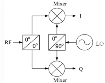
Figure 1-1: Schematic of an I/Q mixer……….……...1
Figure 2.1: A directional coupler……….…....4
Figure 2.1-1: Even mode.……….………...……….…...5
Figure 2.1-2: Odd mode……….………….…5
Figure 2.1-3: The excitation is decomposed into even mode and odd mode excitation (a)Original excitation (b) even mode excitation (c) odd mode excitation……….6
Figure 2.3-1: Examples of non-uniform couplers (a)Smooth-edge coupler (b) wiggly coupler………..………...12
Figure 2.3-2: (a) folded Lange Coupler (b) unfolded Lange Coupler ….……….….13
Figure 2.3-3: Unfolded six-finger coupler………..………....13
Figure 2.3-4: Uniform folded six-finger coupler (unit: mil)………...14
Figure 2.3-5: S parameters of uniform folded six-finger coupler………..………….…15
Figure 2.3-6: Input impedance of the coupler (a) magnitude of Zinreal part of Zin (c) imaginary part of Zin………..……….…16
Figure 2.3-7: Non-uniform folded six-finger coupler (unit: mil)..………..………17
Figure 2.3-8: Input impedance of the coupler, which its ground is replace by a meander ground (a) magnitude of Zin (b) real part of Zin (c) imaginary part of Zin………..……….18
Figure 2.3-9: S parameters of non-uniform folded ………..………..19
six-finger coupler with meander ground Figure 2.4-1: First method to achieve loose-coupling CPW coupler .………20
Figure 2.4-2: Second method to achieve loose-coupling CPW coupler…...………...21
Figure 2.4-3: Loose-coupling CPW coupler and its dimension (unit: mil) …………..……..22
Figure 2.4-4: S parameters of loose-coupling CPW coupler (a) with center ground strip cutted (b) without center ground strip cutted ……..………...…..23
Figure 2.4-5: Phase difference of loose-coupling CPW coupler .………...……23
Figure 2.5-1: Three-section quadrature hybrid’s layout and dimension.……….24
Frgure 2.5-2: Simulation result of three-section coupler ..………..25
Figure 2.5-3: (a) amplitude balance of the coupler (b) phase difference of the coupler………..26
Figure 2.6-1: Photograph of the fabricated three-section 3-dB directional coupler ..……….27
Figure 2.6-2: Measured response of the proposed hybrid ……..………27
Figure 2.6-3: Measured amplitude errors of the proposed directional coupler …..…………28
Figure 3.2-1: The design parameters of two-section wilkinson power divider………32
Figure 3.2-2: Simulation result of the wilkinson power divider.. .………...33
Figure 3.3-1: Measurement result of wilkinson power divider………34
Figure 3.3-2: Photograph of the fabricated two-section wilkinson power divider …………..34
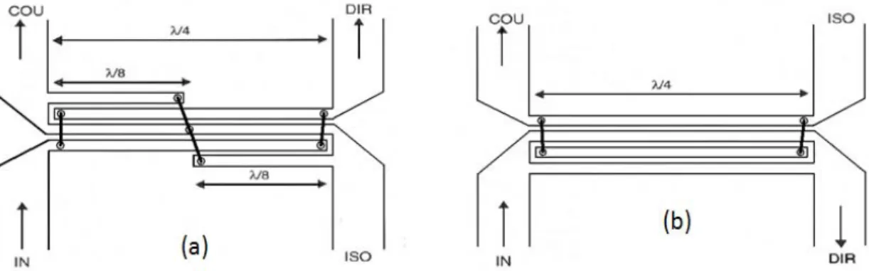
Figure 4.1-1: Block diagram of a single-balanced mixer ………...……….36
Figure 4.1-2: Typical forward I-V Characteristics of a diode………..37
Figure 4.2-1: March's version of rat-race coupler……….40
Figure 4.2-2: Twist between signal and ground path………41
Figure 4.3-1: Conversion loss versus RF frequency. ( Local at difference port )……….43
Figure 4.3-2: LO to RF isolation and RF to IF isolation ( Local at difference port )………...44
Figure 4.3-3: Conversion loss versus IF frequency for fixed LO frequency. ( Local at difference port ) ……….44
Figure 4.3-4: Conversion loss versus LO power………..45
Figure 4.3-5: P1dB ( Local at difference port ) ………45
Figure 4.3-6: Conversion loss versus RF frequency. ( Local at sum port) ………..46
Figure 4.3-7: LO to RF isolation and RF to IF isolation ( Local at sum port )……….46
Figure 4.3-8: Conversion loss versus IF frequency for fixed LO frequency ( Local at sum port ) ………..47
Figure 4.3-9: photograph of the proposed single-balanced mixer………48
Figure 5-1: The photograph of the I/Q mixer………49
Figure 5.1-1: Conversion loss versus RF frequency ( LO (11dBm) is excited from 90 degree hybrid and RF (0dBm) is excited from the power divider )………...50
Figure 5.1-2: Conversion loss versus RF frequency ( LO (11dBm) is excited from the power divider hybrid and RF (0dBm) is excited from 90 degree hybrid )…….51
Figure 5.1-3: Conversion loss versus LO power ( LO from 90o hybrid ; RF from power divider ;IF=5 MHz ; RF<LO )………..51
Figure 5.1-4: LO = 2GHz; RF = 1995 MHz ; IF = 5 MHz………..52
Figure 5.1-5: LO = 3GHz; RF = 2995 MHz ; IF = 5 MHz………..52
Figure 5.1-6: LO = 4GHz; RF = 3995 MHz ; IF = 5 MHz………..53
Figure 5.1-7: LO = 5GHz; RF = 4995 MHz ; IF = 5 MHz………..53
Figure 5.1-8: LO = 6GHz; RF = 5995 MHz ; IF = 5 MHz………..54
Figure 5.1-9: Second method to check the phase difference between two outputs of I/Q mixer………54
Chapter 1
Introduction
I/Q mixer is an important component in modern communication system. It is essential in homodyne transceiver. In this thesis a minimized wideband I/Q mixer is fabricated with following specification.
RF bandwidth:2-6 GHz LO bandwidth:2-6 GHz LO power:15±3 dBm IF bandwidth:DC-200MHz
I-Q phase difference when down conversion is performed:90±10 degree
The circuit should be integrated in a one inch by one inch Al O substrate with a dielectric constant of 9.8, so circuit size is an important factor when designing each subcircuit. There are three component to form an I/Q mixer. Figure 1-1 show the schematic of an I/Q mixer.
An I/Q mixer consist of one power divider, one quadrature coupler and two mixers. The two IF output will have a 90 degree phase difference. The wideband directional coupler is the most difficult part of the whole circuit. Multi-section quadrature coupler technique will be used. From [1], at least three sections can satisfy a 100% fractional bandwidth. There are some problems that we have to solve. First, in order to achieve tight coupling at the center section, the line width and slot width would be very small. Second, the discontinuity effect between each coupled line section should be as small as possible. Third, the difference between even mode and odd mode phase velocity should not be too large. In center section of the three-section coupler, 6-line lange coupler is applied to achieve tight coupling and the proposed meander ground strip can improve the return loss performance. The design procedure and measurement results will be displayed in chapter 2.
In chapter 3, a two-section Wilkinson power divider is fabricated. Compared with other subcircuits, this part is much simpler. It is a great help to minimize circuit size if CPW transmission line is used.
The bandwidth specification of this I/Q mixer has a 100% fractional bandwidth. It is hard for conventional I/Q mixer to achieve such a wide bandwidth or the bandwidth is depicted as IF bandwidth not RF and LO bandwidth. Besides, there are many I/Q mixer’s IF bandwidth cannot start from DC. Problems described above are the main issue when we choose the structure of the mixer. In chapter 4, a single-balanced mixer is designed and realized.
In chapter 5, three devices are combined to form an I/Q mixer. The measurement methods and results are displayed.
Chapter 2
A wideband 3-db directional coupler
Couplers can be found in almost every RF system. In particular, the 3-dB quadruature coupler is an indispensable building block in a large number of RF circuits such as balanced amplifiers, balanced mixers, frequency discriminators, phase shifters, (de)modulators, and feeding networks in antenna arrays. CPW structures facilitate devices to be grounded with low inductance, avoiding via holes. The difference between even and odd mode phase velocities in a CPW directional coupler is very small, which gives better directivity and a better performance when compared to the microstrip based directional coupler
In this chapter a quadrature 3-dB coupler is designed and fabricated. Because of the specification of the IQ mixer, the coupler must be operated over 2-6GHz. The natural choice for an extended bandwidth coupler is the multi-section line coupler. The most challenging part of the multi-section quadrature 3-dB coupler is its tight middle section and to minimize the discontinuity effect between the lose coupling outside sections and the middle section. According to [1], at least three sections are needed to satisfy bandwidth requirement and appropriate ripple level. The interesting part of this coupler is the meander ground at the middle section which make our design more flexible.
2.1 Theory
Figure 2.1: A directional coupler
A directional coupler has four ports , which are labeled as “Input”,“Direct”, ” Coupled” and “Isolated”. There are three parameters to describe the characteristic of the directional coupler .
Coupling(dB) = 10log
PPDirectivity(dB) = 10log
PPIsolation(dB) = 10log
PPWhere P is the input power at port 1, P and P are the output power at port 3 and port 4, respectively .In an ideal case , there is no power transmitted out at the isolation port. In practice, a small amount of power transfers from the Coupled port to the Isolation port.
If we assume a TEM mode propagation, then the electrical characteristics of the coupled line can be determined by the phase velocity and the effective capacitance between the line.
Z =
CZ =
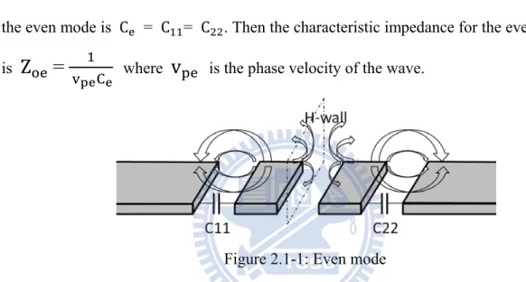
CThe schematic of a directional coupler is shown in Fig 2.1-1. Since it’s a symmetric structure, we can analyze the circuit by using even- and odd-mode analysis. Fig 2.1-1 and Fig 2.1-2 show a CPW couple line with even mode and odd mode excitation.
For the even mode, the electric field has even symmetric about the center line, and no current flow between two conductors. The capacitance of either line to ground for the even mode is C = C = C . Then the characteristic impedance for the even mode is
Z =
C where
v
is the phase velocity of the wave.Figure 2.1-1: Even mode
For the odd mode, the electric field has odd symmetric about the center line. Virtual ground exist between two conductors. We can imagine this as a ground plane through the middle of C . Hence, the effective capacitance of either conductor to ground for the odd mode is C = C + 2C . The characteristic impedance for the odd mode is
Z =
C where
v
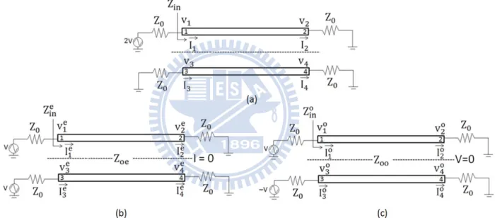
is the phase velocity of the waveA pair of coupled line form a four-port device with two planes of reflection symmetry, As a result, the scattering matrix of this four port device has only 4 independent elements. S S S S S S S S S S S S S SS SS
In performing the even mode and odd mode analysis will be to determine the scattering parameters. To accomplish this, we need to determine voltage V , i 1 … 4, By applying superposition V V V , i 1 … 4
Figure 2.1-3: The excitation is decomposed into even mode and odd mode excitation (a) Original excitation (b) even mode excitation(c) odd mode excitation
Z
Z
Z Z θ Z Z θZ
Z
Z Z θ Z Z θv
Z Z Zv v
Z Z Zv
I
V Z ZI
V Z ZZ
V I V V I IZ
Z Z Z Z Z ZIf we let
Z
Z Z and replace it into Z and Z
Z
Z
Z Z θZ Z θ
Z
Z
Z Z θZ Z θ
Z Z
Z Z
Z
And Z reduce to Z . Because it’s a symmetric structure, all ports will be matched
as long as
Z
Z Z
is satisfied. To obtainV :
V
V
V
V
Z Z Z Z Z Z(∵V
V , V
V )
Z Z Z Z Z θ Z Z Z θ Z Z Z θ Z Z Z Z θZ Z Z Z Z Z θ Z Z Z Z θ
V
V
Z Z θ Z Z Z Z θV
ZZ ZZ θ Z Z Z Z θdefine
C
ZZ ZZV
V
C θ C θTo obtain
V :
V
V
V
V
V
0
To determine V :
Because V V V , we derive V V by using ABCD matrix
V I cos θ jZ sin θ j 1 Z sin θ cos θ V I
V
cos θ V
Z Z ZjZ sin θ
Z V ZV
cos θ V
Z ZZ Z ZZ Z θ θj sin θ V
Z Z ZZ Z Z Z θ θFor the same reason
V :
V
cos θ V
Z ZZ Z ZZ Z θ θj sin θ V
Z Z ZZ Z Z Z θ θV
V
V
cos θ V
Z Z Z Z θ Z Z Z Z θj sin θ V
Z Z Z Z θ Z Z Z Z θcos θ V
Z Z θ Z Z θ θ Z Z Z Z θcos θ V
Z Z Z Z θ Z Z Z Z θ θ Z Z Z Z θcos θ V
Z Z Z Z θ Z Z Z Z θ θ Z Z Z Z θcos θ V
Z Z Z Z θ Z Z Z Z θReplace
C
Z ZZ Z
into the equation then:
cos θ V
CCombining the results derived above, we find that at center frequency the scattering matrix of our coupled-line coupler is
S 0 j 1 C j 1 C 0 C 0 0 C C 0 0 C 0 j 1 C j 1 C 0
Multi-section coupled-line coupler:
where C CN, C CN , etc.
In order to achieve wideband performance, we can add multiple coupled lines in series.We typically design the coupler such that it is symmetric, because the phase relationship has a significant property that it is independent of frequency, where ∠S =∠S 90 at all frequency. Due to this property, applications for which symmetrical couplers are best suited including multiplexers, directional filiters, blanced mixers phase shifters, diplexers, and others to which the 90 degree phase difference property is essential.
2.2 Design procedure and realization
Coupler specification:z Center frequency = 4GHz z Mean coupling = 3dB z Operating frequency = 2~6GHz
One of the most important, yet the most difficult part of the IQ mixer is the wideband quadrature 3-dB coupler. The conventional approach to develop a wideband quadrature hybrid coupler is using stripline structure. The stripline structure has advantages of equal even- and odd-mode effective dielectric constants. That is the same with the assumption of theoretical analysis describe in [1]. Nevertheless, stripline needs complicate and accurate mechanical housing, otherwise the performance degrades. Most of striplines use a low dielectric substrate (ε =2.2 ) to reduce the sensitivity of housing dimensions. As a consequence, the circuit size is relatively large.
To solve the problem mentioned above, we propose a coplanar waveguide structure to realize an ultra-broadband quadrature coupler. The CPW can not only use high dielectric constant substrate to shrink the circuit size but also easy to fabricate without complicated mechanical housing. The CPW allows different geometrical dimensions to minimize the discontinuity effect between coupling sections.
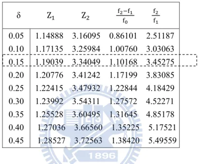
The theory of a multi-section quadrature hybrid [1] had been investigated completely, and the design is tabled into the even- and odd-mode characteristic impedances of each section. The design table is reproduced in Table 2.1. According to the studies, a three-section TEM mode cascaded coupler is required to achieve the desired bandwidth and ripple level. The following table shows the parameters of a
three-section coupler. δ is the ripple level and Z , Z are the normalized even mode impedance of each section. Once the even mode characteristic impedances are known, the normalized odd mode impedance is derived by Z Z and also the coupling in dB of various sections of the coupler as given in Table 2.2. In the following section we describe the design details of each section.
Table 2.1: Table of parameters of three-section symmetrical TEM coupled transmission line directional couplers.
Z &Z Z
Z (Ω) 59.51 167
Z (Ω) 42 14.97
Coupling(dB) -15.2 -1.56
pass band ripple level ±0.15
fractional bandwidth 1.1016
bandwidth ratio 3.4527
Table 2.2: Design parameters of three-section directional couplers δ Z Z 0.05 0.10 0.15 0.20 0.25 0.30 0.35 0.40 0.45 1.14888 3.16095 0.86101 2.51187 1.17135 3.25984 1.00760 3.03063 1.19039 3.34049 1.10168 3.45275 1.20776 3.41242 1.17199 3.83085 1.22415 3.47932 1.22844 4.18429 1.23992 3.54311 1.27572 4.52271 1.25528 3.60495 1.31645 4.85178 1.27036 3.66560 1.35225 5.17521 1.28527 3.72563 1.38420 5.49559
2.3 Three-section coupler
- section 2
The two natural choices for an extended bandwidth coupler will either be the uniform multi-section line coupler or the non-uniform line coupler. The uniform multi-section line coupler is simple in its design, but the sharp discontinuities between various sections, together with the even- and odd-mode velocity difference, degrade the accuracy of the coupling response and isolation at high frequencies, as shown by a number of examples in the literature [2][3]. The non-uniform line coupler [4][5][6] yields better performance.
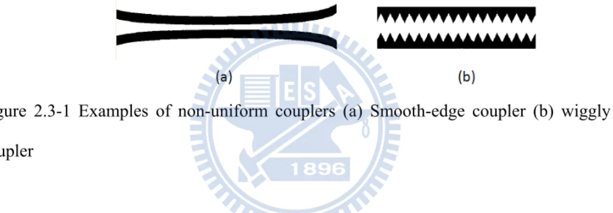
Figure 2.3-1 Examples of non-uniform couplers (a) Smooth-edge coupler (b) wiggly coupler
The high coupling at the center section (1.5dB) can be achieve by several method. One solution is to use tandem type coupler [7]. Although this type of coupler can achieve tight coupling, it require large circuit size and hence more conductor loss. As a result we prefer Lange Coupler [8], which is often used traditionally to achieve strong coupling. The Lange coupler has the advantage of small size, relatively large coupled line spacing, and wider bandwidth, when compared with Branch Line Coupler.
Figure 2.3-2 (a) folded Lange Coupler (b) unfolded Lange Coupler
Lange couplers consist of very narrow coupled lines of a quarter wavelength coupled in parallel to allow fringing on both sides of the line to contribute to the coupling. To increase the coupling it is necessary to use very narrow gaps or more fingers. From [1], the odd mode impedance of the center section is very low (15Ω). At least six fingers are needed to achieve such low odd mode impedance. There are three major parameters to design the coupler, the signal line width (W), slot width (S), and the gap between the signal line and the ground (G).
Figure 2.3-3 Unfolded six-finger coupler
The simulation is carried out by Sonnet and Advance Design System 2009. General speaking, the total performance of the coupler is largely affect by center section. As a result, it will be a great help to design the S11 of the center section as low as we can.
Figure 2.3-4 Uniform folded six-finger coupler (unit: mil)
Figure 2.3-4 show a conventional folded six-finger coupler. The ground is set to be a thin line (4 mils) because high even mode impedance is needed. The center frequency of the specification is 4GHz and the length of the corresponding quarter wavelength is about 320mil. It is difficult to make the total length of three-section coupler within 1000 mil (The PCB size limitation of 1000X1000 mil). Hence the center frequency was shifted to higher frequency to get a small circuit size. The even mode impedance of this circuit is 167Ω and the odd mode impedance is 15Ω. The simulation result is as follow.
Term Term4 Z=50 Ohm Num=4 Term Term2 Z=50 Ohm Num=2 S12P SNP2 File="6finger_couppler_W2_S1.75_L260.s12" 2 3 10 11 12 7 8 9 4 5 6 Ref 1 Term Term3 Z=50 Ohm Num=3 Term Term1 Z=50 Ohm Num=1
Figure 2.3-5 S parameters of uniform folded six-finger coupler
The average return loss (S ) is in the order of -22dB, and it get worse in the high frequency band (-17dB) due to unequal even and odd mode phase velocity. For a fix line width and slot width, it is hard to make return loss better than -25dB. After we get S from the simulation above
,
the input impedance at port 1 can be derived byZ
Z
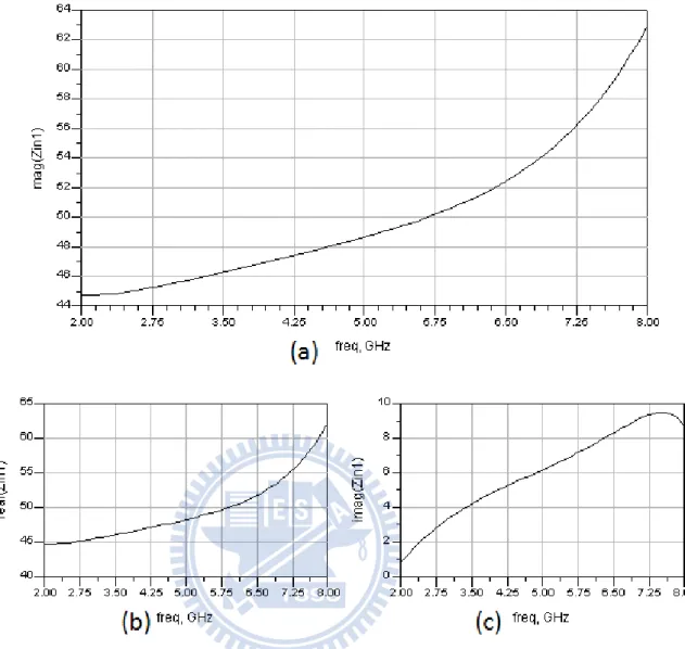
SFigure 2.3-6 Input impedance of the coupler (a) magnitude of Z (a) real part of Z (c) imaginary part of Z
The input impedance rise quickly as the frequency increase which cause large impedance mismatch, especially in high frequency band. That’s cause the return loss get worse quickly at high frequency band.
Figure 2.3-7 Non-uniform folded six-finger coupler (unit: mil)
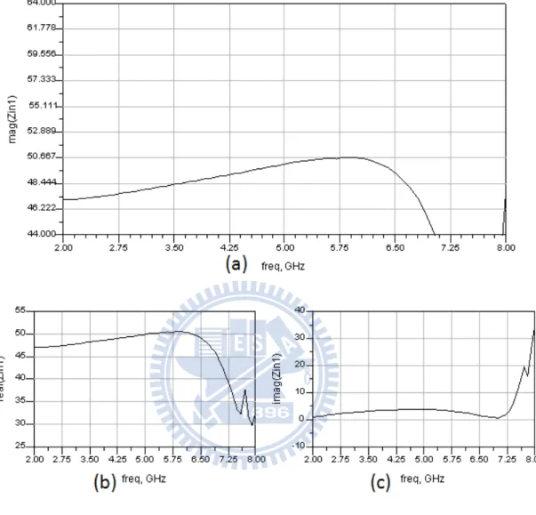
Therefore, it is a motivation to find a way to compensate this phenomenon and the solution is shown in figure 2.3-4. The ground line is replaced by a meander shape line but the line width, slot width are fixed. There are now two extra parameters A and B can be tuned (shown in figure). The even mode impedance of this circuit is 167.3Ω and the odd mode impedance is 14.95Ω. The input impedance affected by the meander ground and can be seen in figure2.3-8.
Figure 2.3-8 Input impedance of the coupler, which its ground is replace by a meander ground (a) magnitude of Z (b) real part of Z (c) imaginary part of Z
As can be seen from the figure above, a deep is produced in the high frequency band. The position of this deep can be changed by tuning parameters A and B. Hence we can make the input impedance around 50Ω that is exactly what we want. The result of S parameter is shown in figure 2.3-9.
Figure 2.3-9 S parameters of non-uniform folded six-finger coupler with meander ground
The average return loss (S ) in the passband now is in the order of -29dB, which is better than the previous circuit. In contrast to the circuit without meander ground, return loss is better in high frequency band.
2.4 Three-section coupler
- section 1&3
According to Table 2.2, the coupling of section1 and section3 is about -15dB, which is quite loose. There are two ways to realize a loose-coupling CPW coupler.
Method 1:
Figure2.4-1 First method to achieve loose-coupling CPW coupler
The even mode impedance is not high (59.5Ω). As a result, the line width (W) must be large enough and the gap (G) has to be small. Because increasing the line width will also decrease the odd mode impedance, the slot width (S) will be very large. This method can introduce some problems that it is hard to connect it with center section. Besides, this circuit is area consuming.
Method 2:
Figure2.4-2 Second method to achieve loose-coupling CPW coupler
Another approach is to insert a ground strip between the coupled lines which is shown in Figure 2.4-2. This structure will change the distribution of even and odd mode electric field, and the variation amount of distribution of even mode electric field is much more. There are some extra parts of even mode electric field is introduced between the center ground strip and the coupled lines. The even mode impedance is decreased because of the increased equivalent even mode capacitance Z = C ). The odd mode impedance will increase a large amount because the excitance of this ground strip can decrease the equvalent odd mode capacitance.
This structure reduces not only the coupling but also the circuit size. One more advantage is that it is much easier to connect this circuit with center section. Therefore using this loose coupled line structure has less junction discontinuity effect. The actual layout is shown in figure2.4-3.
Figure 2.4-3 Loose-coupling CPW coupler and its dimension (unit: mil)
Even though a very thin center ground strip will increase the odd mode impedance substantially (at least 45Ω). From Table 2.2, the value required of odd mode impedance is 42Ω. Hence, it is difficult to achieve -15.2dB coupling with such high odd mode impedance. Therefore some portion of center ground strip was removed to increase the coupling between two coupled lines. After we get the desired odd mode impedance, the required even mode impedance can be achieve by tuning the gap between the coupled line and the outer ground (3mil in this case).The even mode impedance of this circuit is 58.8Ω and the odd mode impedance is 42.3. The center ground strip is cutted by 24 mil and the effect on S parameter is shown in figure 2.4-4.
Figuer 2.4-4 S parameters of loose-coupling CPW coupler (a) with center ground strip cutted (b) without center ground strip cutted
The effect of the cutted center ground strip can be seen as figure above. The center frequency is 4.5GHz and the coupling in high frequency band is much higher than low frequency band that will result the total coupling of the three-section coupler at high frequency band . The phase difference of the coupler is shown in figure2.4-5.
2.5 Three-section coupler
– total cascaded circuit
The design of each section is complete, so we can cascade them one by one. The dimension of section 1 and section 3 is same as previous but the meander ground of center section was varied to get a better performance. Circuit dimension is shown in figure 2.5-1 and the bond wire is remove for simplicity.
Figure 2.5-1 Three-section quadrature hybrid’s layout and dimension. ( unit: mil )
As can be seen from the above figure that the discontinuity between section 1 and section 2 is small due to insertion of ground strip in section 1 and section 3. The ideal circuit length is 960mil (320mil × 3 at 4GHz center frequency). In consider of circuit size, the total length of quadrature coupler is shrinked to 804 mil. Hence the center frequency is also shifted.
EM simulation of this quadrature coupler is carried out by Sonnet, and the result is shown in figure 2.5-2. The phase difference and amplitude balance is shown in figure 2.4-3.
Frgure 2.5-2 Simulation result of three-section coupler
As can be seen in figure above, the coupling of the coupler is below through at low frequency band and didn’t row off in high frequency band. It is designed deliberately because we didn’t consider the metal thickness of the conductor when running simulations. The effect of the metal thickness will decrease the odd mode impedance when the gap between the strips is small enough. The even mode impedance will also larger than actual even mode impedance because of the exsistance of the electrical box when running simulation with Sonnet.
Therefore the actual coupling will be higher than than the simulation result. And the reason why coupling is higher than through in high frequency band can be seen from figure 2.4-4. The coupling of the section 1 and 3 are strong in the corresponding frequency band.
Although the circuit length was shrinked and the center frequency was shifted to higher frequency rather than 4GHz, the performance of the coupler in the desired band is still acceptable. The amplitude balance and phase difference is shown in figure 2.5-3. The amplitude error is less than 1dB and the phase error is smaller than 1.3 over the designed frequency of 2-6 GHz.
Degree dB Figure 2.5-3 (a) amplitude balance of the coupler (b) phase difference of the coupler
2.6 Three-section coupler
– measurement
The photograph of the proposed three-section directional coupler is shown in Figure 2.6-1. The circuit is fabricated on a Al O substrate with a dielectric constant of 9.8 and thickness of 15 mil. The measurement result is shown in figure 2.6-2
Figure 2.6-1 Photograph of the fabricated three-section 3-dB directional coupler
As can be seen in figure 2.6-2, the coupling is slightly greater than through and the reason has been discussed previously. The measured amplitude balance between port 2 (through port) and port 3 (coupled port) is shown in figure 2.6-3. The measured amplitude error is better than 0.75dB over the designed frequency of 2-6 GHz.
Figure 2.6-4 Measured phase inbalance of the proposed directional coupler
The measrued phase error is shown as above. The phase balance is about 88 2 . The phase of the coupled and direct port has a 90 degree difference due to its symmetric. Because the non-uniform coupler in the center section is used (mender ground), the circuit will not be perfect symmetric. Hence the phase error is a little bit larger.
The meander ground in center section provide good impedance matching between different sections at all desired frequency band. Good impedance matching is the main difference between traditional coupler and the proposed coupler. It is usually the reason why we can get better performance only when they simulate the coupler individually and cascade them to get the result, but the performance get worse at high frequency when they simulate it as a whole.
Chapter 3
Wilkinson power divider
In order to make IQ mixer operate appropriately. A three port device with two output signal has equal phase and amplitude is required. The T-junction and wilkilson power divider [9] is commonly used. T-junction’s two ouput ports has no isolation and if the resistive divider is used, there are some extra loss have to be consider. Hence the wilkinson power divider become the best choose for the IQ mixer.
Because the circuit is fabricated with coplanar waveguide (CPW) structure, it has more advantages than microstrip based wilkinson power divider. The coupling between two quarter wavelength transmission line can be reduce by the ground of CPW. Hence a small circuit size can be achieve and the difficulty of circuit design is diminished.
3.1 Theory
The wilkinson power divider is a three-port device with a scattering matrix of:
S 0 j/√2 j/√2 j/√2 j/√2 0 0 00
Note this device is matched at port 1 (S 0), and we find that magnitude of column 1 is:
|S |+|S |+|S |=1
Thus, just like the lossless divider the incident power on port 1 is evenly and efficiently divided between the outputs of port 2 and port 3:
P |S | P P
2 P |S | P P
2
We also note that the port 2 and 3 of this device are matched. S S 0
The resister is the secret to the Wilkinson power divider, and is the reason that it is matched at ports 2 and 3, and the reason that port 2 and port 3 are isolated. Single section Wilkinson power divider can reach 60% fractional bandwidth. In order to increase the bandwidth of the power divider, we used muti-section struction again.
3.2 Design procedure and realization
S. B. Cohn has provided some tables for designing multi-section wilkinsion power divider [10]. A 100% bandwidth with return loss and isolation around -27dB can be achieve by a three-section structure. Unfortunately, we can’t afford more room for such long structure. By preliminary studies, we decided to used two section Chebyshev response structure. On one hand, it won’t be too long; on the other hand, the performance is acceptabe. The circuit-level simulation is carried out by Advanced Design System 2009 and we get EM simulation result from Sonnet. This power divider is fabricated on a Al O substrate with a dielectric constant of 9.8 and thickness of 15 mil. The dimension of each section is shown in figure 3.1-1.
The EM simulation result is shown in figure 3.2-2. The return loss (S ) and isolation (S ) is below -21dB for the desired frequency band which is still acceptable. Because the wilkinson power divider is a symmetry structure, the amplitude balance and phase balance is guaranteed to be good which is essential for RF input signal of IQ mixer. The center frequency is a little higher than 4GHz because the length of power divider is shrinked.
3.3 Measurement
The measurement result is shown in figure 3.3-1. The return loss and isolation is better than -15dB at the desired frequency band (2-6 GHz) and the through is around -3.1dB. The photograph of the circuit is shown in figure 3.3-2.
Figure 3.3-1 Measurement result of wilkinson power divider
Chapter 4
single-balanced mixer
The IQ-mixer contains two balanced mixers and a phase shifting hybrid. General speaking a wideband diode mixer is designed in balanced type structure. The balanced mixer in the construction consists of two identical single ended mixers with a 3dB hybrid junction(90 or 180 degrees) to produce either better input VSWR or better LO/RF isolation. The balanced mixer using a 90o hybrid generates good RF VSWR, but poor LO/RF isolation. Using a 180o hybrid suppress all even harmonics of both LO and RF siganls, thus yielding a very low conversion loss. Among all 180o hybrids. The three-port balun only provides the out-of-phase power splitting without good output port-to-port isolations and return losses. These properties make the rat race ring in the balanced circuits better than the balun.
To achieve compact circuit size and wider bandwidth, the size of the mixer was reduced by using phase inverter in the ring arm. Moreover, the place of the diodes was deposit inside the ring. In this chapter a single-balanced mixer with finite ground CPW (FCPW) on 15 mils Al2O3 substrate is designed and fabricated.
4.1 Theory
A single-balanced diode mixer uses two diodes. Either the LO drive or the RF signal is balanced, adding destructively at the IF port of the mixer and providing inherent rejection. The level of rejection is dependent on the amplitude and phase balance of the balun, providing the balanced drive, and the matching between the two diodes. Other advantages of a singly-balanced design are rejection certain mixer spurious products, depending on the exact configuration, and suppression of Amplitude Modulated (AM) LO noise. AM noise could be a significant problem in early microwave and mm-wave receivers where the available LO sources were very noisy. Modern wireless transceivers tend to make use of synthesised LO drives and the LO phase noise gives more of a problem than the AM noise.
One disadvantage of balanced designs is that they require a higher LO drive level. Figure 4.1 shows a block diagram of a single-balanced mixer.
Figure 4.1-1 Block diagram of a single-balanced mixer
The LO drive to the two diodes is in anti-phase and the RF signal is in-phase. If the mixing products are at mRF ± nLO, this mixer will reject all spurious products where m is even. The reason can be seen below. Figure 4.1-2 shows the typical I-V characteristics of a Schottky diode, which can be described by equation (4.1).
I a V a V a V a V (4.1)
Figure 4.1-2 Typical forward I-V Characteristics of a diode
The current through each diode is depicted as below.
I a V a V a V a V
I a V a V a V a V
The minus sign in (4.3) is due to that LO drive to the two diodes is in anti-phase. V VRcos ωRt VLcos ωLt (4.2)
The IF current is:
IIF i i a V V a V V a V V a V V … (4.4)
Then replace (4.2) and (4.3) into (4.4).
IIF a 2VRcos ωRt a 4VR VLcos ωRt cos ωLt
a 2VRcos ωRt 6VRVL cos ωRt cos ωLt
a 8VR VLcos ωRt cos ωLt 8 VRVLcos ωRt cos ωLt
2a VRcos ωRt 2a VRVL cos ωR ωL t cos ωR ωL t
a VR cos 3ω
Rt VRVLcos ωR 2ωL t VRVLcos ωR 2ωL t
VR cos ωRt a VRVLcos 3ωR ωL t VRVLcos 3ωR ωL t
VRVL cos ωR 3ωL t VRVLcos ωR 3ωL t
3 VRVL VRVL cos ωR ωL t cos ωR ωL t
The IF output has the frequency component:
ωR, ωL, ωR ωL , ωR 2ωL , 3ωR ωL , ωR 3ωL …
As can be seen that the even order harmonic of RF signal will be eliminated if RF input is placed at sum port of the single-balanced mixer.
Similarly, if the RF drive were in anti-phase and the LO in-phase, all spurious products with n even would be rejected. The anti-phase signal is also cancelled at the IF port, because the LO drive should be at a significantly higher level than the RF signal, it is often chosen as the anti-phase signal to increase the LO to IF isolation.
The RF short-circuit, shown at the IF port in Figure 4.1-1 is required for the mixer to work appropriately. If the RF impedance at the IF port were high, the RF signal voltage across the diodes would be small and the mixer's conversion loss would be very high. The LO signal, however, does not require a low impedance at the IF port. Because the LO is a balanced signal across the diode pair, the common port of the diodes is a virtual ground to the LO. The LO drive across the two diodes adds destructively to a null at the common port, as if it were grounded. In most cases, the LO and the RF are comparatively close in frequency, so the RF short circuit will also be a good LO short circuit.
The design procedure for a balanced diode mixer is similar to that for a single-ended. The only difference is that the balun structure providing the RF and LO isolation. As described in [11], which provide a technique to enhance the isolation performance of the rat race coupler. One option for the balun realization is a rat-race coupler. This is a very popular option at microwave frequencies where it is a comparatively small structure that can be produced inexpensively on a printed substrate.
4.2 Circuit design
The rat race ring is a widely used 180o hybrid coupler. Its drawbacks are its large size and limited bandwidth. The limiting factor in the hybrid ring coupler is the three-quarter wavelength section, which restricts the useful frequency range for the 180° hybrid to f0 ± 0.23f0 where f0 is the center frequency in the band of interest . Numerous publications have been produced to improve the performance of this type of coupler.
Several design techniques have been proposed to enhance the useful bandwidth and to reduce its size. In [12] one quarter wavelength section with phase reversal was used to replace the three-quarter wavelength line. This phase-reversal section was realized with parallel coupled lines with two diagonal grounded ends (show in figure 4.2-1). Such a modified coupler achieved more than one-octave bandwidth. Although the bandwidth increases considerably, the even-mode impedance required for the coupled section would be too large to be realized, which is difficult to fabricate by using conventional chemical etching technique.
The conventional rat-race hybrids are inherently narrowband structures. This bandwidth limitation was attributed to the narrowband phase inverter within the quarter-wavelength and
3/4–wavelength line section. Many efforts have been made to make the bandwidth of rat-race ring coupler larger [13][14]. Most of them pay their attention by making a broadband phase inverter.
The finite- ground-plane CPW (FCPW) is a good candidate to realize this ideal phase inverter, because the “hot” lines as well as the ground planes are located on the upper surface of the carrier material. This enables parallel implementation of active and passive lumped elements into the circuit without any via hole structure, which results in a significant simplification in manufacturing process.
Figure 4.2-2 Twist between signal and ground path
Even if an ideal phase inverter is used, the conventional rat-race ring coupler with 70.7Ω ring impedance and Butterworth-type response is still limited to of about 74% fractional bandwidth for return loss better than 15 dB. The ring coupler contain an ideal phase inverter can show a Chebyshev-type response of order two. For 12 dB return loss, the ring coupler with 55Ω ring impedance has 100% fractional bandwidth.
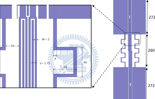
Because of the crossover at the ring arm, the signal line of the rat-race ring is DC grounded. We must use RF virtual ground to terminate two diodes and the IF signals are picked up from these RF virtue ground. The design parameters and circuit dimensions are list in Table 4.2-1.
Strip width (mil) Slot width (mil) Finite ground width (mil) Ring arm impedance(54Ω) 4 2 4
50Ω impedance 4.2 1.8 12
Table 4.2 Design parameters and circuit dimensions of the rat-race ring
This single-balanced mixer is fabricated on 15mil Al2O3 substrate with center frequency 4GHz and 100% fractional bandwidth. The RF virtual ground can be formed by an FCPW open stub or shunt a capacitor. Here we used a 2pF capacitor at the IF port. The diodes used in the mixer are Metelics silicon schottky diodes (MSS30,242-B20). In view of the layout of the IQ mixer, we squeeze the single-balanced mixer. The effect of the bond wires at crossover can be compensated by shortening the corresponding ring arms about 5 mils.
4.3 Measurement
There are two ways to excite the single-balanced mixer. One is to excite Local source at sum port and the other is to excite it at difference port. The measurement results are shown in the following figures respectively.
Figure 4.3-2 LO to RF isolation and RF to IF isolation ( Local at difference port )
Figure 4.3-3 Conversion loss versus IF frequency for fixed LO frequency. ( Local at difference port )
Figure 4.3-4 Conversion loss versus LO power
Figure 4.3-6 Conversion loss versus RF frequency. ( Local at sum port )
Figure 4.3-8 Conversion loss versus IF frequency for fixed LO frequency. ( Local at sum port )
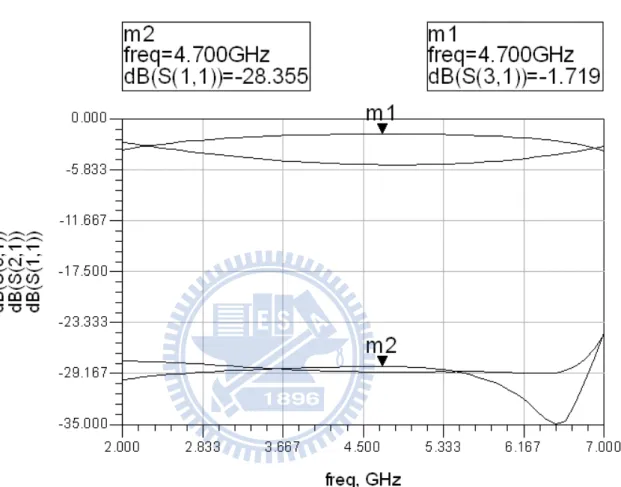
The conversion loss is around 8dB over the desired RF frequency band and it’s better when RF signal is excited at difference port. In this case, RF signal is virtual ground at IF port that causes the voltage across the diodes would be larger, hence the conversion loss would be smaller.
The RF to LO isolation is provided by the ring because RF port is also the virtual ground of the LO signal and vice versa. From figure 4.3-2, the RF to IF isolation is poor compared with figure 4.3-6. Because RF and IF are both placed at sum port, the ring provides no inherent isolation. The isolation here is only provided by a 2pF shunt capacitor. One way to solve this problem is to use a sharp low pass filter rather than just one order at IF port. From figure 4.3-6, the RF to IF isolation is better when RF is placed at difference port because the IF port is the virtual ground of the RF signal and the effect of the capacitor (RF-short circuit) The photograph of the circuit is shown in figure 4.3-8.
Figure 4.3-9 photograph of the proposed single-balanced mixer
Chapter 5
I/Q mixer
In this chapter, three device ( coupler, power divider, single-balanced mixer) are constituted to form the I/Q mixer. The whole circuit is fabricated in a one inch by one inch Al2O3 substrate. The measurement result will display in the following section. The photograph of the circuit is shown in figure 5-1.
Figure 5-1 The photograph of the I/Q mixer
5.1 Measurement
Figure 5.1-1 shows the conversion loss versus RF frequency. The conversion loss at the desired frequency band is around 12dB. The CH1 and CH2 are the outputs of the I/Q mixer which is shown in figure 5-1.
Figure 5.1-1 Conversion loss versus RF frequency ( LO (11dBm) is excited from 90 degree hybrid and RF (0dBm) is excited from the power divider )
Figure 5.1-2 shows the conversion loss versus RF frequency The conversion at the desired frequency band is around 12dB too.
Figure 5.1-2 Conversion loss versus RF frequency ( LO (11dBm) is excited from the
power divider hybrid and RF (0dBm) is excited from 90 degree hybrid )
Figure 5.1-3 Conversion loss versus LO power ( LO from 90o hybrid ; RF from power divider ;IF=5 MHz ; RF<LO )
There are two methods to check that the two outputs of the I/Q mixer have 90 degree phase difference. First, we can just excite the desired RF and LO signal in a fixed frequency and see the result. If LO is 2GHz and RF is 1995MHz. Two outputs of the I/Q mixer is shown in figure 5.1-4.
Figure 5.1-4 LO = 2GHz; RF = 1995 MHz ; IF = 5 MHz
As can be seen the two outputs has a phase difference 90 degree. The following figures show the results with different LO and RF frequency.
Figure 5.1-6 LO = 4GHz; RF = 3995 MHz ; IF = 5 MHz
Figure 5.1-8 LO = 6GHz; RF = 5995 MHz ; IF = 5 MHz The second method can be shown in figure 5.1-9.
Figure 5.1-9 Second method to check the phase difference between two outputs of I/Q mixer
The RF and LO of the I/Q mixer is excited by a signal which its frequency change with time. The two outputs will produce DC voltage (cosθ , sinθ) because RF frequency is equal to LO frequency. The delay line in the upper path is essential for this method, because it introduce a phase delay. The phase delay is changed with frequency of the input signal because a same delay line saw different electric length at different frequency. Hence the DC outputs will also change with time. Figure 5.1-10 show the measurement result of second method.
Figure 5.1-10 Measurement result of second method.
The difference between the first method and the second method is that the first method can only see the phase difference and amplitude balance at some fixed frequency. The second method can see the results over all frequency components.
Chapter 6
Conclusion
This thesis has demonstrated a minimized wideband I/Q mixer on a one inch by one inch Al O substrate with a dielectric constant of 9.8.
In chapter 2, miniaturized wideband quadrature hybrid coupler has been realized by using three-section cascaded CPW coupler structure. The return loss would be better if the meander ground in the center section is used. The way to tune the meander ground is to let the input impedance around 50Ω, because the deep in the input impedance diagram can change if the dimension of the meander is changed. In consider of the area limitation, the length of the coupler is shrinked and the center frequency is shifted to higher frequency.
In chapter 3, a wideband wilkinson power divider is fabricated. Because the circuit is in CPW based, the coupling between two paths can be reduce by insert a ground strip between them. Hence, the circuit size is reduced.
In chapter 4, a single-balanced mixer is fabricated. The 180 degree hybrid in the mixer is chosen as a rat race ring coupler. To realized a wideband rat race ring, we can replace the 3/4 wavelength transmission line by a 1/4 wavelength transmission and a phase inverter which not only widen the bandwidth but also reduce the circuit size. To further reduce the circuit size, the diodes is placed inside the ring and the RF virtual ground is form by a shunt 2pF capacitor.
In chapter 5, the circuits fabricated in previous chapter are combined to form an I/Q mixer. There are two ways to check the phase and magnitude difference between two outputs of I/Q mixer. The measurement result is shown in figures and the specification is achieved.
References
[1]E. G. Cristal and L. Young, “Theory and tables of optimum symmetrical TEM-Mode
coupled transmission line directional couplers,” IEEE Trans. Microwave Theory Tech.,
vol. MTT-13, no. 5, pp. 544–558, Sep. 1965
[2]J. S. Izadian, “A new 6–18 GHz, 3dB multi-section hybrid coupler using asymmetric
broadside, and edge coupled lines,” in IEEE MTT-S Int. Microwave Symp. Dig., 1989,
pp. 243–246.
[3] G. Kemp, J. Hobdell, and J. W. Biggin, “Ultra-wideband quadrature coupler,”
Electron. Lett., vol. 19, no. 6, pp. 197–198, 1983.
[4] S. Uysal and H. Aghvami, “Synthesis, design, and construction of ultra-wide-band
nonuniform quadrature directional couplers in inhomogeneous media,” IEEE Trans.
Microwave Theory Tech., vol. 37, pp. 969–975, June 1989.
[5] “Improved wideband 3dB nonuniform directional coupler,” Electron. Lett., vol. 25, no. 8, pp. 541–542, Apr. 1989.
[6] Duncan K.Y.Lasu, Steve P.March, Lionel E.Davis and Robin Sloam, “Simplified
design technique for high performance microstrip multi-section couplers”, IEEE Trans.
[7] T. Y. Chang, C. L. Liao, and C. H. Chen, “Novel uniplanar tandem couplers,” in Proc. 32nd Eur. Microwave Conf., 2002, pp. 127–130.
[8] R. M. Osmani, ‘Synthesis of Lange couplers,’ IEEE Trans. Microwave Theory and Techn.
Vol. 29, Feb. 1981, pp
[9] Wilkinson, E.J., “An N-way hybrid power divider,” IRE Trans. Microw. Theory Technol., 1960, MTT-8, pp. 116–118
[10] S. B. Cohn, “A class of broadband three-port TEM-mode hybrids, ”. IEEE Tram.Microwave Theory Tech., vol. MTT-16, Feb. 1968, PP. 110-116
[11] Walker, J.L.B. ”Improvements to the Design of the 180 Rat Race Coupler and its
Application to the design of Balanced Mixers with High LO to RF Isolation”, IEEE
MMT-S Digest, 1997, Vol. II, pp 747-750
[12]S. March, “A wide band stripline hybrid ring,” IEEE Trans. Microwave Theory
Tech., vol. MTT-16, p. 361, June 1968.
[13]T. Wang Z. OU and K. Wu, “Experimental study of wideband uniplanar phase
inverters for MICs” in IEEE MTT-S Int. Microwave Symp. Dig., 1997, pp777-780
[14]T. Wang and K. Wu, “Size-reduction and band-broadening design technique of
uniplanar hybrid ring coupler using phase inverter for M(H)MIC’s,” IEEE Trans.