國 立 交 通 大 學
電子工程學系 電子研究所碩士班
碩 士 論 文
系統層級靜電放電感測器設計
Transient Detection Circuit for
System-Level ESD Protection
研 究 生 : 石弼嘉
指導教授 : 柯明道 教授
系統層級靜電放電感測器設計
Transient Detection Circuit for
System-Level ESD Protection
研 究 生: 石弼嘉
Student : Pi-Chia Shih
指導教授: 柯明道 教授
Advisor : Prof. Ming-Dou Ker
國立交通大學
電子工程學系 電子研究所碩士班
碩士論文
A Thesis
Submitted to Department of Electronics Engineering & Institute of Electronics
College of Electrical Engineering and Computer Science
National Chiao-Tung University
in Partial Fulfillment of the Requirements
for the Degree of
Master
in
Electronics Engineering
Sept. 2005
Hsin-Chu, Taiwan, Republic of China
系統層級靜電放電感測器設計
學生:石弼嘉 指導教授:柯明道 教授
國立交通大學
電子工程學系 電子研究所碩士班
ABSTRACT (CHINESE)
摘要
隨著半導體製程技術與積體電路設計的進步,電子產品的運作與控制大都已經使 用積體電路晶片來操作。藉由高積集度積體電路的使用,再輔以軔體及軟體的功效, 電子系統具有更多樣與更精密的功能。為了增進積體電路的運算速度與降低晶片製造 的成本,積體電路中的電晶體尺寸也隨著製程演進而逐漸縮小,而這也使得積體電路 對靜電放電(Electrostatic Discharge, ESD)的耐受度下降,也容易在靜電放電的瞬間對積體電路造成破壞。所以ESD 在電子產品良率及可靠度上扮演相當重要的角色。
為了防護 ESD 對積體電路的破壞,可從下面幾點著手。首先是提升元件本身的
ESD 防護能力,亦即針對防護「人體放電模式標準(Human Body Model, HBM)」,「機 器放電模式標準(Machine Model, MM)」及「元件充電模式標準(Charged Device Model, CDM)」ESD 保護元件及電路等設計。再來是加強製造、封裝、測試、組裝、及運輸 等環境的靜電放電防制(Electrostatic Discharge Control, ESDC),減少靜電源的產生。此 類相關ESDC 文件規範可參考 ESD Association standard ANSI/ESD S20.20-1999。最後, 當積體電路已經安裝到系統電路版上時,在正常工作情形下,還要通過電磁共容 (Electromagnetic Compatibility, EMC)的法規管制,而在電磁共容測試標準裡,有一項 測試經常造成電子系統的故障,這項測試就是「系統規格之靜電放電測試(System-level ESD Test)」,(IEC 61000-4-2 : Electromagnetic Compatibility (EMC), Part 4-2 : Testing and measurement techniques – Electrostatic discharge immunity test)。
統層級靜電放電感測電路。此感測電路的目的是考慮系統層級靜電放電時,利用此感 測電路偵側靜電的發生並記錄,再配合其它軔體或軟體的使用,使電路在受到靜電干
擾而故障時,能自動作出回復的動作。量測方式採用 IEC 61000-4-2 標準,以水平耦
合板進行接觸放電測試。同時,測試進行時利用電容及暫態電壓抑制器(Transient Voltage Suppressors, TVS)當雜訊過濾器,以量測電路耐受度與保護元件之相對關係。
Transient Detection Circuit for
System-level ESD Protection
Student: Pi-Chia Shih Advisor: Prof. Ming-Dou Ker
Department of Electronics Engineering & Institute of Electronics
National Chiao-Tung University
ABSTRACT (ENGLISH
)
ABSTRACT
Electrical products are used in every aspect of lives, such as providing communication, all forms of entertainment, luxurious lifestyles, life support, etc. Of all items listed, communication systems and life support rank highest in the areas of concern when interference comes from unintentional sources. As the size of IC process keeps on scaling down, electrical products are more sensitive to the interference. Control of EMC (electromagnetic compatibility) is an increasing necessity. Correct application of design methods ensures reliable operation, reduces project timescales, and helps meet regulatory requirements. However, ESD (Electrostatic Discharge) is the major source of interference.
Generally speaking, there are two kinds of ESD specifications. The first specification is component-level ESD specification. In this specification, three models are shown bellow: human body model (HBM), machine model (MM), and charge device model (CDM). The second one is system-level ESD specification. Recently, most international companies adopt the standard, named IEC 61000-4-2 : Electromagnetic Compatibility (EMC), Part 4-2 : Testing and measurement techniques – Electrostatic discharge immunity test. The major difference between component-level ESD specification and system-level ESD specification
is that whether the devices under test (EUT) with or without power supply.
A system-level transient voltage detection circuit is designed in 0.13-μm 3.3-V 1P8M CMOS process. The detection circuit is used to detect and memorize the occurrence of ESD stress. For the complete function of the proposed transient detection circuit under system-level ESD test, this detection circuit must operate with a firmware to reset the circuit or other further application after the ESD stress. In addition, different types of board-level noise filter networks are evaluated for their effectiveness to improve the immunity of the device under test under system-level ESD test.
誌謝
ACKNOWLEDGE ACKNOWLEDGEMENT
首先要感謝的是我的指導教授柯明道博士。老師以其本身嚴謹的研究態度以及超 乎常人的研究熱情,讓我於這兩年中獲得最珍貴的研究心態與方法。而在老師開明的 指導以及豐沛的研究資源下,我不但能盡情將研究的電路下線驗證,也由於所從事的 論文研究具實用性。除此之外,老師亦提供相當充裕的研究經費使我在這兩年中不至 於生活匱乏而能更努力的從事我的碩士論文研究。畢業之後無論從事任何研究我都將 會僅記老師的至理名言:Smart = 做事要有效率,成果要有水準。 接著要感謝的是一起打拼的同學們,宗信、靖驊、建樺、鍵樺、啟祐、諭哥、家 瑩、煒明、志朋、峻帆、傑忠、岱原、宗熙、邰佑、建文、晉元,大家一起做研究、 出遊、唱歌,讓我在苦悶的研究生活中增添不少樂趣。我也要感謝實驗室陳世倫學長、 陳榮昇學長、張瑋仁學長、徐新智學長、陳世宏學長、林昆賢學長、黃彥霖學長、鄧 至剛學長、顏承正學長、許勝福學長、王文泰學長。他們無論是在論文研究的瓶頸或 是晶片量測的疑難雜症上都給了我很多的方向及幫助,使我能更順利的完成我的碩士 論文。 另外,要感謝的是張智毅學長、李彥枏學長,感謝他們對我在研究上的支持與幫 助。還要再次感謝許勝福學長、顏承正學長在量測時給我許多協助。 最後要感謝我的父母。感謝他們多年來默默的關心與支持,在我最需要的時候給 予最大的幫助,使我能勇往向前,一路走來直至今日。生命中的貴人甚多,不可勝數, 我將秉持著感恩的心,盡最大的能力幫助也即將展開論文研究的學弟妹們。 石弼嘉 九十四年九月Content
ABSTRACT
(CHINESE)...
IABSTRACT
(ENGLISH) ...
IIIACKNOWLEDGEMENT ...
VC
ONTENT...
VIIT
ABLEC
APTIONS...
IXF
IGUREC
APTIONS...
XC
HAPTER1
I
NTRODUCTION... 1
1.1 BACKGROUND...1 1.2 MOTIVATION...1 1.3 TESTING MODEL...21.3.1 Component-level ESD Specification... 3
1.3.2 System-level ESD Specification ... 3
1.4 THESIS ORGANIZATION...3
C
HAPTER2
I
NTRODUCTION OFIEC
61000-4-2
S
PECIFICATIONS... 7
2.1 BACKGROUND...7
2.2 OVERVIEW...7
2.3 TEST GENERATOR...8
2.3.1 Characteristics and Performance of the ESD Generator... 8
2.3.2 Verification of the Characteristics of the ESD Generator... 9
2.4 TEST LEVELS...9
2.5 TEST SET-UP...9
2.5.1 Test set-up for tests performed in laboratories... 10
2.5.1.1. Table-top Equipment... 11
2.5.1.2. Floor-standing Equipment... 11
2.5.1.3. Test Method for Ungrounded Equipment... 11
2.5.2 Test Set-up for Post-installation Tests ... 13
2.6 TEST PROCEDURE...13
2.6.1 Laboratory Reference Conditions... 13
2.6.1.1. Climatic Conditions... 14
2.6.1.2. Electromagnetic Conditions ... 14
2.6.2 EUT Exercising... 14
2.6.3 Execution of the Test ... 14
2.6.4 Direct Application of Discharges to the EUT... 15
2.6.5 Indirect Application of the Discharge... 17
2.6.5.2. Vertical Coupling Plane ... 18
2.7 EVALUATION OF TEST RESULTS...18
2.8 TEST REPORT...19
C
HAPTER3
D
ESIGN OFT
RANSIENTD
ETECTIONC
IRCUIT... 25
3.1 INTRODUCTION...25
3.2 REFERENCE CIRCUIT...26
3.3 SIMULATION OF TRANSIENT DETECTION CIRCUIT...27
3.4 CONCLUSION...30
C
HAPTER4
M
EASUREMENT... 47
4.1 MEASUREMENT SETUP...47 4.2 TEST STRUCTURE...49 4.3 MEASUREMENT RESULT...51 4.4 CONCLUSION...52C
HAPTER5
S
UMMARY ANDF
UTUREW
ORK... 65
5.1 SUMMARY...65
5.2 FUTURE WORKS...66
R
EFERENCES:... 68
Table Captions
T
ABLE1.1
IEC
61000-4-2
CRITERIA... 4
T
ABLE2.1
S
PECIFICATIONS OFESD
GENERATOR. ... 21
T
ABLE2.2
W
AVEFORM PARAMETERS. ... 21
T
ABLE2.3
T
EST LEVELS. ... 22
T
ABLE2.4
D
ISCHARGE TYPE... 22
T
ABLE4.1
T
HE MEASUREMENT RESULT OF TRANSIENT DETECTION CIRCUIT UNDERESD
STRESS... 53
Figure Captions
F
IG.
1.1
S
CHEMATIC DIAGRAM OF HUMAN BODY MODEL(HBM). ... 5
F
IG.
1.2
S
CHEMATIC DIAGRAM OF CHARGED DEVICE MODEL(CDM). ... 5
F
IG.
1.3
S
CHEMATIC DIAGRAM OF MACHINE MODEL(MM). ... 5
F
IG.
1.4
S
YSTEM-
LEVELEMC/ESD
TEST ONLCD
PANEL OF NOTEBOOK BY ANESD
GUN. ... 6
F
IG.
2.1
S
IMPLIFIED DIAGRAM OF THEESD
GENERATOR. ... 23
F
IG.
2.2
D
ISCHARGE ELECTRODES OF THEESD
GENERATOR. ... 23
F
IG.
2.3
T
YPICAL WAVEFORM OF THE OUTPUT CURRENT OF THEESD
GENERATOR... 24
F
IG.
2.4
E
XAMPLE OF TEST SET-
UP FOR TABLE-
TOP EQUIPMENT–
LABORATORY TESTS. ... 24
F
IG.
3.1
C
ONVENTION CIRCUIT DIAGRAM OFESD
SENSOR. ... 31
F
IG.
3.2
S
IMULATION RESULT OF THEESD
SENSOR(
NOISE ATV
DD). ... 31
F
IG.
3.3
S
IMULATION RESULT OF THEESD
SENSOR(
NOISE ATG
ND). ... 31
F
IG.
3.4
C
IRCUIT DIAGRAM OF DETECTION CIRCUIT(NMOS). ... 32
F
IG.
3.5
C
IRCUIT DIAGRAM OF DETECTION CIRCUIT(PMOS)... 32
F
IG.
3.6
S
IMULATED RESULT OF DETECTION CIRCUIT(1)
(V
DD). ... 33
F
IG.
3.7
S
IMULATED RESULT OF DETECTION CIRCUIT(2)
(V
DD). ... 33
F
IG.
3.8
S
IMULATED RESULT OF DETECTION CIRCUIT(3)
(G
ND). ... 33
F
IG.
3.9
S
IMULATION RESULTS OF DIFFERENT NOISE PEAK OFV
DD(Q
=
6). .... 34
F
IG.
3.10
S
IMULATION RESULTS OF DIFFERENT NOISE PEAK OFV
DD(Q
=
1/6). . 34
F
IG.
3.11
N
OISE PEAK OFV
DD VS.
PARAMETERQ
(1/2)... 35
F
IG.
3.12
N
OISE PEAK OFV
DD VS.
PARAMETERQ
(2/2)... 35
F
IG.
3.13
S
IMULATION RESULTS OF DIFFERENT NOISE PEAK OFV
DD(
COUPLING CAPACITANCE:
0.1
PF)... 36
F
IG.
3.14
S
IMULATION RESULTS OF DIFFERENT NOISE PEAK OFV
DD(
COUPLING CAPACITANCE:
3
PF)... 36
F
IG.
3.15
N
OISE PEAK OFV
DD VS.
COUPLING CAPACITANCE. ... 37
F
IG.
3.16
S
IMULATION RESULTS OF DIFFERENT NOISE PEAK OFG
ND(Q
=
6). .... 37
F
IG.
3.17
S
IMULATION WAVEFORMS OF DIFFERENT NOISE PEAK OFG
ND(Q=1/6)... 38
F
IG.
3.18
N
OISE PEAK OFG
ND VS.
PARAMETERQ
(1/2)... 38
F
IG.
3.19
N
OISE PEAK OFG
ND VS.
PARAMETERQ
(2/2)... 39
F
IG.
3.20
N
OISE PEAK OFG
ND VS.
CAPACITANCE. ... 39
F
IG.
3.21
T
YPICAL MEASURED NOISE WAVEFORM ONV
DD OFCMOS
IC
WITHESD
VOLTAGE OF–
800
V
UNDER SYSTEM-
LEVELESD
TEST... 40
F
IG.
3.22
U
NDERDAMPED SINE WAVE VOLTAGE USED INHSPICE
TOSIMULATED THE NOISE VOLTAGE UNDER SYSTEM
-
LEVELESD
TEST. .. 40
F
IG.
3.23
S
IMULATION RESULTS OF DIFFERENT CORNERS(
NOISE ATV
DD). ... 41
F
IG.
3.24
S
IMULATION RESULTS OF DIFFERENT CORNERS(
NOISE ATG
ND). ... 41
F
IG.
3.25
S
IMULATION RESULTS OF DIFFERENT CORNERS(
NOISE AT BOTHV
DD ANDG
ND)... 42
F
IG.
3.26
ESD
COUPLING PATH... 42
F
IG.
3.27
S
IMULATION RESULTS OF DIFFERENT CORNERS:
NOISE ATV
DD ANDG
ND(1/8)... 43
F
IG.
3.28
S
IMULATION RESULTS OF DIFFERENT CORNERS:
NOISE ATV
DD ANDG
ND(2/8)... 43
F
IG.
3.29
S
IMULATION RESULTS OF DIFFERENT CORNERS:
NOISE ATV
DD ANDG
ND(3/8)... 44
F
IG.
3.30
S
IMULATION RESULTS OF DIFFERENT CORNERS:
NOISE ATV
DD ANDG
ND(4/8)... 44
F
IG.
3.31
S
IMULATION RESULTS OF DIFFERENT CORNERS:
NOISE ATV
DD ANDG
ND(5/8)... 45
F
IG.
3.32
S
IMULATION RESULTS OF DIFFERENT CORNERS:
NOISE ATV
DD ANDG
ND(6/8)... 45
F
IG.
3.33
S
IMULATION RESULTS OF DIFFERENT CORNERS:
NOISE ATV
DD ANDG
ND(7/8)... 46
F
IG.
3.34
S
IMULATION RESULTS OF DIFFERENT CORNERS:
NOISE ATV
DD ANDG
ND(8/8)... 46
F
IG.
4.1
D
IE PHOTO OF THE TRANSIENT DETECTION CIRCUIT... 54
F
IG.
4.2
L
AYOUT VIEW OF THE TRANSIENT DETECTION CIRCUIT. ... 54
F
IG.
4.3
M
EASUREMENT SETUP OF THE SYSTEM-
LEVELESD
TEST WITHINDIRECT CONTACT
-
DISCHARGE TEST MODE... 55
F
IG.
4.4
M
EASUREMENT INSTRUMENTS. ... 55
F
IG.
4.5
T
OP VIEW OFPCB
PHOTO... 56
F
IG.
4.6
M
EASUREDV
DD,
I
DD ANDOUT
WAVEFORMS OF THE RINGOSCILLATOR
,
FOR THEESD
GUN WITHESD
VOLTAGE OF–
800
V
ZAPPING ON THE
HCP... 56
F
IG.
4.7
N
OISE FILTER NETWORK... 57
F
IG.
4.8
(
A)
D
EVICE CROSS-
SECTIONAL VIEW AND(
B)
LAYOUT TOP VIEW OF THESCR
STRUCTURE FOR SYSTEM-
LEVELESD
TEST... 57
F
IG.
4.9
(
A)
C
IRCUIT DIAGRAM AND(
B)
LAYOUT TOP VIEW OF THEF
IG.
4.10
M
EASUREMENT WAVEFORM OFSCR
STRUCTURE UNDERESD
STRESS
... 58
F
IG.
4.11
C
ORRELATIONS BETWEEN MEASUREMENTTLU
LEVELS ANDDECOUPLING CAPACITANCES WITH TWO
SCR
STRUCTURES... 59
F
IG.
4.12
C
ORRELATIONS BETWEEN MEASUREMENTTLU
LEVELS ANDBREAKDOWN VOLTAGES OF
TVS
WITH TWOSCR
STRUCTURES. ... 59
F
IG.
4.13
M
EASUREMENT WAVEFORMS OF THE RING OSCILLATOR CIRCUITUNDER
ESD
STRESS... 60
F
IG.
4.14
C
ORRELATIONS BETWEEN MEASUREMENTTLU
LEVELS ANDDECOUPLING CAPACITANCES WITH RING OSCILLATOR
. ... 60
F
IG.
4.15
C
ORRELATIONS BETWEEN MEASUREMENTTLU
LEVELS ANDBREAKDOWN VOLTAGE OF
TVS
WITH THE RING OSCILLATOR... 61
F
IG.
4.16
M
EASUREMENT WAVEFORMS OF TRANSIENT DETECTION CIRCUITUNDER
ESD
STRESS... 61
F
IG.
4.17
P
ARASITIC CAPACITANCES OF POWER PADS... 62
F
IG.
4.18
S
IMULATION RESULTS OF THE TRANSIENT DETECTION CIRCUIT WITH–
20
V
NOISE VOLTAGE(
CASE1). ... 62
F
IG.
4.19
S
IMULATION RESULTS OF THE TRANSIENT DETECTION CIRCUIT WITH+
20
V
NOISE VOLTAGE(
CASE1). ... 63
F
IG.
4.20
S
IMULATION RESULTS OF THE TRANSIENT DETECTION CIRCUIT WITH–
20
V
NOISE VOLTAGE(
CASE2). ... 63
F
IG.
4.21
S
IMULATION RESULTS OF THE TRANSIENT DETECTION CIRCUIT WITH+
20
V
NOISE VOLTAGE(
CASE2). ... 64
F
IG.
4.22
T
HE PARASITIC CAPACITANCE OFTVS. ... 64
F
IG.
5.1
F
LOWCHART OF THEPOR
AND TRANSIENT DETECTION CIRCUITDURING POWER
-
ON... 67
F
IG.
5.2
F
LOWCHART OF THEPOR
AND TRANSIENT DETECTION CIRCUITC
HAPTER
1
I
NTRODUCTION
.
1.1 B
ACKGROUNDWhen the sweaters are taken off in dry winter, the phenomenon of electrostatic discharge (ESD) occurs. Most of the time, people are charged to a high voltage level by triboelectric charging, usually due to rubbing contacts between their shoes or clothing and dissimilar materials used for flooring, storage, and the like. These words give rise to images of lightning strikes or the sparks that leap from one’s fingertips when touching a doorknob in dry winter. The sparks are the result of the ionization of the air gap between the charged human body and the zero-potential surface of the doorknob. In other words, the phenomenon of ESD occurs around. In the semiconductor industry, as the process and technology developed, the size of integrated circuits (IC) became scaledown and more complex. The potentially destructive nature of ESD in ICs became more apparent. The high voltages result in large electric fields and high current densities in the small devices, which can lead to breakdown of insulators and thermal damage in the IC. The losses in the IC industry caused by ESD can be substantial if no efforts are made to understand and solve the problem. The largest category is that of electrical overstress (EOS), of which ESD is a subset. In many cases, failures classified as EOS could actually be due to ESD, which would make this percentage even higher.
1.2 M
OTIVATIONEMC specifications of the IC products. As the result, IC designers devote to the study of electromagnetic compatibility (EMC) issues. However, as the IC process developed, control of EMC is an increasing necessity. Correct application of design methods ensures reliable operation, minimizes liability risk, reduces project timescales, and helps meet regulatory requirements. The best time to consider all aspects of EMC is during the preliminary design cycle, long before the first circuit is incorporated on a schematic, the first instruction written for a software program, or the outline of a mechanical chassis drawn.
Recently, ESD issue plays an important role in IC design field. ESD is a high-amplitude event that causes permanent damage, latent failures, or disruption in functional operation. Accordingly, performing an ESD test is a powerful method of determining potential failures. The problem of static electricity accumulation and subsequent discharges becomes more relevant for uncontrolled environments. In addition, the widespread application of equipment and systems in various environments exist. The effects of operator discharge can cause a simple malfunction of equipment or damage of electrical components. The power-line noise detection circuit presented in this paper is used to correct the malfunction of electrical components.
1.3 T
ESTINGM
ODELGenerally speaking, there are two kinds of ESD specifications. The first specification is component-level ESD specification. In this specification, three models are shown bellow: human body model (HBM), machine model (MM), and charge device model (CDM). The second phase is system-level ESD specification. Recently, most international companies adopt the standard, IEC 61000-4-2 [1]. Whether the devices under test (EUT) with or without power supply is the major difference between system-level ESD specification and component-level ESD specification.
1.3.1 Component-level ESD Specification
The various models used for testing a device's ESD sensitivity (ESDS) level, i.e., HBM, CDM, and MM, apply standard waveforms to electrically stress the device under ESD testing. These waveforms are usually defined by their peak current level, rise and fall times, and duration. Figs. 1.1 ~ 1.3 show the various waveforms and basic test circuits used in HBM, CDM, and MM testing, respectively.
1.3.2 System-level ESD Specification
There are many products with protection circuits that they can pass the component-level ESD specification. However, these products may not pass the standard of system-level ESD specification. As the result, system-level ESD specification becomes more important. IEC 61000-4-2 was adopted in this paper during the testing. The test set-up consists of the test generator, EUT and auxiliary instrumentation necessary to perform direct and indirect application of discharges to the EUT in the following manner:
a. contact discharge to the conductive surfaces and to coupling planes; b. air discharge at insulating surfaces.
Contact discharge was adopted in this paper to perform the measurement. The detail of IEC 61000-4-2 would show in chapter 2.
1.4 T
HESISO
RGANIZATIONThe chapter 2 of the thesis specifies the standard of system-level ESD test. The measurement setup and methods are presented. In chapter 3, a transient detection circuit is described and simulation results are shown there. In chapter 4, the test structure and the measurement result are presented. The last chapter summarizes this thesis.
Table 1.1 IEC 61000-4-2 criteria.
Criterion Performance Result
Level A EUT is unaffected by ESD stress. Pass
Level B EUT works abnormally during ESD
stress, but it will reset automatically. Pass
Level C EUT works abnormally after ESD
stress, but it needs to be reset manually. Failure
Fig. 1.1 Schematic diagram of human body model (HBM).
Fig. 1.2 Schematic diagram of charged device model (CDM).
C
HAPTER
2
I
NTRODUCTION OF
IEC
61000-4-2
S
PECIFICATIONS
2.1 B
ACKGROUNDESD is a powerful source of interference that can cause electronic systems to reset, lose date, or fail to operate. As the result, customers always require that product should operate flawlessly at both designers’ site and customers’ site after ESD tests. So, there are many kinds of standards which define test environment, equipment, test methods, and so on. Designers are always required to prove that their product can withstand ESD. They should also test their products under the conditions close to the environment in which customers will use it. Every international company would require that their product should pass IEC 61000-4-2 specification.
2.2 O
VERVIEWThis standard specifies the immunity requirements and test methods for electrical and electronic equipment subjected to static electricity discharges, from operators directly, and to adjacent objects. It additionally establishes test procedures and defines ranges of test levels which relate to different environmental and installation conditions.
The object of this standard is to establish a common and reproducible basis for evaluating the performance of electrical and electronic equipment when subjected to electrostatic discharges. In addition, it includes electrostatic discharges which may occur from personnel to objects near vital equipment.
- typical waveform of the discharge current; - range of test levels;
- test equipment; - test set-up; - test procedure.
This standard specifies test performed in “laboratories” and “post-installation tests” performed on equipment in the final installation. However, this standard does not intend to give specifications for the tests which are applied to particular apparatus or systems. The objective of this standard is to give a general basic reference to all concerned product committees of the IEC. The product committees (or users and manufacturers of equipment) remain responsible for the appropriate choice of the tests and the severity level to be applied to their equipment. A simplified diagram of the ESD generator is given in Fig. 2.1.
In order not to impede the task of coordination and standardization, the product committees or users and manufacturers are strongly recommended to consider (in their future work or revision of old standards) the adoption of the relevant immunity tests specified in this standard.
2.3 T
ESTG
ENERATOR2.3.1 Characteristics and Performance of the ESD Generator
The specifications of the ESD generator is shown as table 2.1. The generator shall be provided with means of preventing unintended radiated or conducted emissions, either of pulse or continuous type, so as not to disturb the EUT or auxiliary test equipment by parasitic effects.
The energy storage capacitor, the discharge resistor, and the discharge switch shall be placed as close as possible to the discharge electrode. The dimensions of the discharge tips
are given in Fig. 2.2
2.3.2 Verification of the Characteristics of the ESD Generator
In order to compare the test results obtained from different test generators, the characteristics show in table 2.2 shall be verified using the discharge return cable to be used in the testing. The waveform of the output current of the ESD generator during the verification procedure shall conform to Fig. 2.2. The values of the characteristics of the discharge current shall be verified with 1000 MHz bandwidth measuring instrumentation. A lower bandwidth implies limitations in the measurement of rise time and amplitude of the first current peak. For verification, the tip of the discharge electrode shall be placed in direct contact with the current-sensing transducer, and the generator operated in the contact discharge mode. The ESD generator shall be re-calibrated in defined time periods in accordance with a recognized quality assurance system.
2.4 T
ESTL
EVELSThe preferential range of test levels for the ESD test is given in table 2.3. Testing shall also be satisfied at the lower levels given in table 2.3.
Contact discharge is the preferred test method. Air discharges shall be used where contact discharges cannot be applied. Voltages for each test method are given in tables 1a and 1b. The voltages shown are different for each method due to the differing methods of test. It is not intended to imply that the test severity is equivalent between test methods.
2.5 T
ESTS
ET-
UPThe test set-up consists of the test generator, EUT and auxiliary instrumentation necessary to perform direct and indirect application of discharges to the EUT in the
following manner:
(a) contact discharge to the conductive surfaces and to coupling planes; (b) air discharge at insulating surfaces.
The EUT shall be arranged in accordance with the manufacturer’s instructions for installation.
2.5.1 Test set-up for tests performed in laboratories
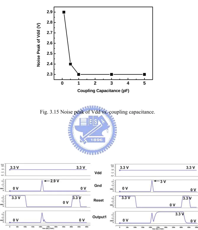
A ground reference plane shall be provided on the floor of the laboratory. It shall be a metallic sheet (copper or aluminum) of 0.25 mm minimum thickness; other metallic materials may be used but they shall have at least 0.65 mm minimum thickness. The minimum size of the reference plane is 1 m2, the exact size depending on the dimensions of the EUT. It shall project beyond the ETU or coupling plane by at least 0.5 m on all sides, and shall be connected to the protective grounding system.
A distance of 1 m minimum shall be provided between the equipment under test and the walls of the laboratory and any other metallic structure. The discharge return cable of the ESD generator shall be connected to the ground reference plane. The total length of this cable is in general 2 m.
In cases where this length exceeds the length necessary to apply the discharges to be selected points, the excess length shall, where possible, be placed non-inductively off the ground reference plane and shall not come closer than 0.2 m to other conductive parts in the test set-up.
The connection of the earth cables to the ground reference plane and all bondings shall be of low impedance, for example by using clamping devices for high frequency applications.
To allow indirect application of the discharge, they shall be constructed from the same material type and thickness as that of the ground reference plane, and shall be connected to
the ground reference plane via a cable with a 470 kΩ resistor located at each end. These resistors shall be capable of withstanding the discharge voltage and shall be insulated to avoid short circuits to the ground reference plane when the cable lies on the ground reference plane.
2.5.1.1. Table-top Equipment
The test set-up shall consist of a wooden table, 0.8 m high, standing on the ground reference plane.
A horizontal coupling plane (HCP), 1.6 m x 0.8 m, shall be placed on the table. The EUT and cables shall be isolated from the coupling plane by an insulating support 0.5 mm thick.
If the EUT is too large to be located 0.1 m minimum form all sides of the HCP, an additional, identical HCP shall be used, placed 0.3 m from the first, with the short sides adjacent. The table has to be enlarged or two tables may be used. The HCPs shall not be bonded together, other than via resistive cables to the ground reference plane.
An example of the test set-up for table-top equipment is given in Fig. 2.4.
2.5.1.2. Floor-standing Equipment
The EUT and cables shall be isolated from the ground reference plane by an insulating support about 0.1 m thick.
2.5.1.3. Test Method for Ungrounded Equipment
The test method described in this subclause is applicable to equipment or part(s) of equipment whose installation specifications or design preclude connection to any grounding system. Equipment, or parts thereof, includes portable, battery-operated and double-insulated equipment (class II equipment).
the EUT shall be removed prior to each applied ESD pulse.The charge on the metallic point or part to which the ESD pulse is to be applied, for example, connector shells, battery charge pins, metallic antennae, shall be removed prior to each applied ESD test pulse.
When one or several metallic accessible parts are subject to the ESD test, the charge shall be removed from the point where the ESD pulse is to be applied, as no guarantee can be given about the resistance between this and other accessible points on the product.A cable with 470 kΩ bleeder resistors, similar to the one used with the horizontal and vertical coupling planes, shall be used.
As the capacitance between EUT and HCP (table-top) and between EUT and GRP (floor-standing) is determined by the size of the EUT, the cable with bleeder resistors may remain installed during the ESD test when functionally allowed. In the discharge cable, one resistor shall be connected as close as possible, preferably less than 20 mm from the EUT test point. The second resistor shall be connected near the end of the cable attached to the HCP for table-top equipment, or GRP for floor-standing equipment.
The presence of the cable with the bleeder resistors can influence the test results of some equipment. In case of dispute, a test with the cable disconnected during the ESD pulse takes precedence over the test with the cable installed during the test, provided that the charge has sufficiently decayed between the successive discharges.
As an alternative, the following options can be used:
- the time interval between successive discharges shall be extended to the time necessary to allow natural decay of the charge from the EUT;
- a carbon fibre brush with bleeder resistors (for example, 2 x 470 kΩ) in the grounding cable;
- an air-ionizer to speed-up the “natural” discharging process of the EUT to its environment.
alternative method shall be reported in the test report.
The tip of the ESD generator shall be held perpendicular to the surface of the EUT.
2.5.2 Test Set-up for Post-installation Tests
These tests are optional, and not mandatory for certification tests; they may be applied only when agreed between manufacturer and customer. It has to be considered that other co-located equipment may be unacceptably affected. The equipment or system shall be tested in its final installed conditions.
In order to facilitate a connection for the discharge return cable, a ground reference plane shall be placed on the floor of the installation, close to the EUT at about 0.1 m distance. This plane should be of copper or aluminum not less than 0.25 mm thick. Other metallic materials may be used, providing the minimum thickness is 0.65 mm. the plane should be approximately 0.3 m wide, and 2 m in length where the installation allows. This ground reference plane should be connected to the protective grounded system. Where this is not possible, it should be connected to the grounded terminal of the EUT, if available.
The discharge return cable of the ESD generator shall be connected to the reference plane at a point close to the EUT. Where the EUT is installed on a metal table, the table shall be connected to the reference plane via a cable with a 470 kΩ resistor located at each end, to prevent a build-up of charge.
2.6 T
ESTP
ROCEDURE2.6.1 Laboratory Reference Conditions
In order to minimize the impact of environmental parameters on test results, the tests shall be carried out in climatic and electromagnetic reference conditions as specified in 2.6.1.1 and 2.6.1.2.
2.6.1.1. Climatic Conditions
In the case of air discharge testing, the climatic conditions shall be within the following ranges:
- ambient temperature: 15 ˚C to 35 ˚C; - relative humidity: 30 % to 60 %;
- atmospheric pressure: 86 kPa (860 mbar) to 106 kPa (1,060 mbar). NOTE Any other values are specified in the product specification.
The EUT shall be operated within its intended climatic conditions.
2.6.1.2. Electromagnetic Conditions
The electromagnetic environment of the laboratory shall not influence the test results.
2.6.2 EUT Exercising
The test programs and software shall be chosen so as to exercise all normal modes of operation of the EUT. The use of special exercising software is encouraged, but permitted only where it ca be shown that the EUT is being comprehensively exercised.
For conformance testing, the EUT shall be continually operated in its most sensitive mode (program cycle) which shall be determined by preliminary testing.
If monitoring equipment is required, it should be decoupled in order to reduce the possibility of erroneous failure indication.
2.6.3 Execution of the Test
The testing shall be performed by direct and indirect application of discharges to the EUT according to a test plan. This should include:
- representative operating conditions of the EUT;
- whether the EUT should be tested as table-top or floor-standing; - the points at which discharges are to be applied;
- at each point, whether contact or air discharges are to be applied; - the test level to be applied;
- the number of discharges to be applied at each point for compliance testing; - whether post-installation tests are also to be applied.
It may be necessary to carry out some investigatory testing to establish some aspects of the test plan.
2.6.4 Direct Application of Discharges to the EUT
Unless stated otherwise in the generic, product-related or product-family standards, the static electricity discharges shall be applied only to those points and surfaces of the EUT which are accessible to persons during normal use. The following exclusions apply (i.e. discharges are not applied to those items):
(a) those points and surfaces which are only accessible under maintenance. In this case, special ESD mitigation procedures shall be given in the accompanying documentation;
(b) those points and surfaces which are only accessible under service by the (end-)user. Examples of these rarely accessed points are as follows: battery contacts while changing batteries, a cassette in a telephone answering machine, etc.;
(c) those points and surfaces of equipment which are no longer accessible after fixed installation or after following the instructions for use, for example, the bottom and/or wallside of equipment or areas behind fitted connectors;
metallic connector shell. In this case, contact discharges shall only be applied to the metallic shell of that connector.
Contacts within a non-conductive (for example, plastic) connector and which are accessible shall be tested by the air-discharges test only. This est shall be carried out by using the rounded tip finger on the ESD generator.
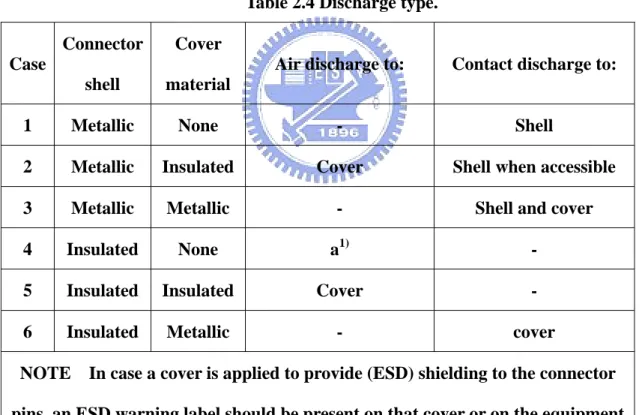
In general, six cases shall be considered in table 2.4.
(e) those contacts of connectors or other accessible parts that are ESD sensitive because of functional reasons and are provided with an ESD warning label, for example, r.f. inputs from measurement, receiving or other communication functions.
Rationale: Many connector ports are designed to handle high-frequency information, either analogue or digital, and there fore cannot be provided with sufficient overvoltage protection devices. In the case of analogue signals, bandpass filters may be a solution. Overvoltage protecting diodes have too much stray capacitance to be useful at the frequencies at which the EUT is designed to operate.
In all previous cases, special ESD mitigation procedures are recommended, to be given in the accompanying documentation. The test voltage shall be increased from the minimum to the selected test level, in order to determine any threshold of failure. The final test level should not exceed the product specification value in order to avoid damage to the equipment. The test shall be performed with single discharges. On preselected points at least ten single discharges (in the most sensitive polarity) shall be applied. For the time interval between successive single discharges an initial value of 1 s is recommended. Longer intervals may be necessary to determine whether a system failure has occurred.
NOTE The points to which the discharges should be applied may be selected by means of an exploration carried out at a repetition rate of 20 discharges per second, or more.
The ESD generator shall be held perpendicular to the surface to which the discharge is applied. This improves repeatability of the test results. The discharge return cable of the generator shall be kept at a distance of at least 0.2 m from the EUT whilst the discharge is being applied. In the case of contact discharges, the tip of the discharge electrode shall touch the EUT, before the discharge switch is operated. In the case of painted surfaces covering a conducting substrate, the following procedure shall be adopted:
If the coating is not declared to be an insulating coating by the equipment manufacturer, then the pointed tip of the generator shall penetrate the coating so as to make contact with the conducting substrate. Coating declared as insulating by the manufacturer shall only be submitted to the air discharge. The contact discharge test shall not be applied to such surfaces.
In the case of air discharges, the round discharge tip of the discharge electrode shall be approached as fast as possible (without causing mechanical damage) to touch the EUT. After each discharge, the ESD generator (discharge electrode) shall be removed from the EUT. The generator is then retriggered for a new single discharge. This procedure shall be repeated until the discharges are completed. In the case of an air discharge test, the discharge switch, which is used for contact discharge, shall be closed.
2.6.5 Indirect Application of the Discharge
Discharges to objects placed or installed near the EUT shall be simulated by applying the discharges of the ESD generator to a coupling plane, in the contact discharge mode.
In addition to the test procedure described in 2.6.5, the requirements given in 2.6.5.1 and 2.6.5.2 shall be met.
2.6.5.1. Horizontal Coupling Plane (HCP) under the EUT
At least 10 single discharges (in the most sensitive polarity) shall be applied at the front edge of each HCP opposite the centre point of each unit (if applicable) of the EUT and 0.1 m from the front of the EUT. The long axis of the discharge electrode shall be in the plane of the HCP and perpendicular to its front edge during the discharge.
The discharge electrode shall be in contact with the edge of the HCP .
In addition, consideration should be given to exposing all sides of the EUT to this test.
2.6.5.2. Vertical Coupling Plane
At least 10 single discharges (in the most sensitive polarity) shall be applied to the centre of one vertical edge of the coupling plane. The coupling p lane, of dimensions 0.5 m x 0.5 m, is placed parallel to, and positioned at a distance of 0.1 m from, the EUT.
Discharges shall be applied to the coupling plane, with sufficient different positions such that the four faces of the EUT are completely illuminated.
2.7 E
VALUATION OFT
ESTR
ESULTSThe test results shall be classified in terms of the loss of function or degradation of performance of the equipment under test, relative to a performance level defined by its manufacturer or the requestor of the test, or agreed between the manufacturer and the purchaser of the product. The recommended classification is as follows:
(a) normal performance within limits specified by the manufacturer, requestor or purchaser;
(b) temporary loss of function or degradation of performance which ceases after the disturbance ceases, and from which the equipment under test recovers its normal performance, without operator intervention;
(c) temporary loss of function or degradation of performance, the correction of which requires operator intervention;
(d) loss of function or degradation of performance which is not recoverable, owing to damage to hardware or software, or loss of data.
The manufacturer’s specification may define effects of the EUT which may be considered insignificant, and therefore acceptable.
This classification may be used as a guide in formulating performance criteria, by committees responsible for generic, product and product-family standards, or as a framework for the agreement on performance criteria between the manufacturer and the purchaser, for example where no suitable generic, product or product-family standard exists.
2.8 T
ESTR
EPORTThe test report shall contain all the information necessary to reproduce the test. In particular, the following shall be recorded:
- the items specified in the test plan required by clause 8 section 2.6 of this standard;
- identification of the EUT and any associated equipment, for example, brand name, product type, serial number;
- identification of the test equipment, for example, brand name, product type, serial number;
- any special environmental conditions in which the test was performed, for example, shielded enclosure;
- any specific conditions necessary to enable the test to be performed; - performance level defined by the manufacturer, requestor or purchaser;
- performance criterion specified in the generic, product or product-family standard;
- any effects on the EUT observed during or after the application of the test disturbance, and the duration for which these effects persist;
- the rationale for the pass/fail decision (based on the performance criterion specified in the generic, product or product-family standard, or agreed between the manufacturer and the purchaser);
- any specific conditions of use, for example cable length or type, shielding or grounding, or EUT operating conditions, which are required to achieve compliance.
Table 2.1 Specifications of ESD generator. Energy storage capacitance (CS + Cd) 150 pF +/- 10 %
Discharge resistance (Rd) 330 Ω +/- 10 %
Charging resistance (RC) Between 50 MΩ and 100 MΩ
Output voltage (note 1) Up to 8 kV (nominal) for contact discharge Up to 15 kV (nominal) for air discharge Tolerance of output voltage indication +/- 5%
Polarity of output voltage Positive and negative (switchable)
Holding time At least 5 sec
Discharge, mode of operation (note 2) Single discharge (time between successive discharges at least 1sec)
Waveshape of discharge current See Fig. 2.3
NOTE 1 Open circuit voltage measured at the energy storage capacitor.
NOTE 2 The generator shold be able to generate at a repetition rate of at least 20 discharges per second for exploratory purposes only.
Table 2.2 Waveform parameters.
Level
Indicated voltage
(kV)
First peak current of discharge +/- 10 % (A) Rise Time tr with discharge switch (ns) Current (+/- 30 %) at 30 ns (A) Current (+/- 30 %) at 60 ns (A) 1 2 3 4 2 4 6 8 7.5 15 22.5 30 0.7 to 1 0.7 to 1 0.7 to 1 0.7 to 1 4 8 12 16 2 4 6 8
Table 2.3 Test levels.
1a – Contact Discharge 1b – Air Discharge
Level Test Voltage (kV) Level Test Voltage (kV)
1 2 3 4 X1) 2 4 6 8 Special 1 2 3 4 X1) 2 4 8 15 Special 1)
“X” is an open level. The level has to be specified in the dedicated equipment specification. If higher voltages than those shown are specified, special test
equipment may be needed.
Table 2.4 Discharge type.
Case
Connector shell
Cover material
Air discharge to: Contact discharge to:
1 Metallic None - Shell
2 Metallic Insulated Cover Shell when accessible
3 Metallic Metallic - Shell and cover
4 Insulated None a1) -
5 Insulated Insulated Cover -
6 Insulated Metallic - cover
NOTE In case a cover is applied to provide (ESD) shielding to the connector pins, an ESD warning label should be present on that cover or on the equipment
near to that connector to which the cover is applied. 1)
“a” : If the product (family) standard requires testing to individual pins of an insulated connector, air discharges shall apply.
Fig. 2.1 Simplified diagram of the ESD generator.
-0.05 ø 12 0 -0.05 ø 8 0 ø 8 50 ± 1
Interchangeable part (tip) Body of generator (Note) 25° to 40° Sharp point -0.05 ø 12 0
Note The Discharge switch (e.g. vacuum relay) shall be mounted as close as possible to the tip of the discharge electrode.
Fig. 2.2 Discharge electrodes of the ESD generator.
I at 60 ns I at 30 ns 10 % 90 % 100 % Ipeak t 30 ns 60 ns tr = 0.7 to 1 ns
Fig. 2.3 Typical waveform of the output current of the ESD generator.
0.1 m VCP 0.5 m x 0. 5 m EUT 0.1 m
Ground Reference Plane
Resistor 470 k? Typical Position for
Indirect Discharge to HCP
Typical Position for Direct Application
Typical Position for Indirect Discharge to VCP Insulation Horizontal Coupling Plane (HCP) 1.6 m x 0.8 m
C
HAPTER
3
Design of Transient Detection Circuit
3.1 I
NTRODUCTIONElectrostatic discharge (ESD) is a high-amplitude event that probably causes permanent damage, latent failures, or disruption in functional operation. Performing an ESD test is a powerful method of determining potential failures over an extremely wide spectrum of frequencies. When applied in a conducted manner, this pulse creates an extremely strong electromagnetic field. Compared to the electrical fast transient (EFT) test, which essentially excites cables, ESD also evaluates box shielding and PCB layout deficiencies as well as manifests currents in cables.
Most of commercial products are performed system-level ESD test for reliability and safety concern [2]. Basically, the IEC 61000-4-2 had specified the criteria and testing method. Actually, ESD level is dependent on customer’s need and applications, and it’s very hard to get a higher level once in a while. During ESD stress, the power of the EUT will be disturbed. Power failure may lead to data loss, malfunction or crash. Therefore, the on-chip ESD protection circuits must be designed to clamp ESD voltages without causing damage in the IC’s. Protection circuits could be developed against component-level ESD stress. However, it may not be developed against system-level ESD stress significantly. As a result, a hardware/firmware co-design can be designed to solve such issue of system-level ESD testing [3].
To avoid the system upset or frozen by the system-level ESD stress, the system should have an auto-detection function to detect such a system-level electrical transient. Once the fast system-level electrical transient is detected in some IC, the system can automatically
reset itself and restore gracefully to a known and stable state. As a result, the firmware must be regularly checking for abnormal conditions. An external hardware timer such as the retriggerable monostable multivibrator is the most effective method of firmware check [4]. However, this method significantly increases the total cost of the electrical/electronic products. To solve this issue, an effective on-chip ESD detector is proposed in this work to detect the system-level electrical transient.
3.2 R
EFERENCEC
IRCUITA circuit was proposed to detect the system-level electrical transient automatically. If the system-level electrical transient is detected in the IC, the microcontroller can automatically reset itself and restore gracefully to a known and stable state. For this purpose, the firmware must be regularly checking for abnormal conditions. The circuit diagram of the on-chip ESD sensor is shown in Fig. 3.1, where two latch logic gates are used as the ESD sensors to detect the system-level electrical transient. The NMOS in the inverters of the sensor_1 in Fig. 3.1 is designed with a larger W/L ratio than that of the PMOS to make the latch easily locking at logic 0. On the contrary, the PMOS in the inverters of the sensor_2 in Fig. 3.1 is designed with a larger W/L ratio than that of the NMOS to make the latch easily locking at logic 1.
The HSPICE simulated results are shown in Figs. 3.2 and 3.3. In Fig. 3.2, the VDD voltage is originally kept at 5 V with a relatively stable VSS of 0 V, but some undershooting glitches from the system-level electrical transient are coupled to the VDD. The first (second) glitch on the VDD voltage waveform in Fig. 3.2 has a rise time/fall time of 1 ns (10 ns) and an undershooting voltage level of – 1.2 V, whereas the sensor output state Q is changed from the logic 0 to logic 1. In Fig. 3.3, the VSS voltage is originally kept at 0 V with a relatively stable VDD of 5 V, but some overshooting glitches from the system-level
electrical transient are coupled to the VSS. The first (second) glitch on the VSS voltage waveform in Fig. 3.3 has a rise time / fall time of 1 ns (10 ns) and an overshooting voltage level of 5 V, whereas the sensor output state Q still maintains at logic 0 after the VSS overshooting transition. The third (fourth) glitch on the VSS voltage waveform in Fig. 3.3 has a rise time / fall time of 1 ns (10 ns) and an overshooting voltage level of is 6.2 V, whereas the sensor output state Q is changed from the logic 0 to logic 1. This sensor was applied in the IC product.
The system-level ESD susceptibility of the IC product has been improved from the original 2 kV (4 kV) to become greater than 8 kV (15 kV) in the contact (air) discharge ESD test method, in spite of the ESD zapping location being on the table or at the PC case. As a result, a transient detection circuit proposed in the next section is used to implement similar function.
3.3 S
IMULATION OFT
RANSIENTD
ETECTIONC
IRCUITThe circuit diagrams of the transient detection circuit are shown in Fig. 3.4 and Fig. 3.5. The latch logic gates are used as the memory to memorize the occurrence of ESD stress. The capacitances are used as the ESD detectors to detect the system-level electrical transient. The NMOS/PMOS enclosed with the dotted lines are used to reset the circuit to the initial state. In these circuits, the device sizes of the latch are designed to make the logic of point A become high easily. In contrast, the W/L ratio of invertors makes point B change state from high to low much easily.
At first, a simple peak on the power of the detection circuit is used to analyze the function of detection circuit. In the initial state, the voltage of Vdd rises to high, the voltage of point A is high, and the voltage of point B is low. When the voltage of Vdd is below the voltage of Gnd, the parasitic diodes of the PMOS such as Mp1, Mp2, Mp3, and Mp4would
be turned on. The voltage between point A (B) and Vdd and would be kept in a constant voltage. Once the power returns to its normal voltage, the following actions will be taken immediately. Capacitances C2 and C4 keep the voltage between point A and Vdd, while C1 and C3 keep it between point B and Gnd in constant voltage. As a result, the voltage of point A would rise to high and the voltage of point B would be pulled to low, leading state of the latch would be changed. Therefore, output would be changed to high state. When reset signal rises to high state, the output would be pulled to the initial state (low). The voltage waveforms during the peak are shown in Fig. 3.7. On the other hand, when the voltage of Gnd is pulled higher than the voltage of Vdd, the parasitic diodes of the NMOS (Mn1, Mn2, Mn3, and Mn4) would be turned on. The voltage between point A (B) and Gnd and would be kept in a constant voltage. Once the power returns to its normal voltage, the following actions will be taken immediately. Capacitances C2 and C4 keep the voltage between point A and Vdd, while C1 and C3 keep it between point B and Gnd in constant voltage. As a result, the voltage of point A would rise to high and the voltage of point B would pull to low. The state of the latch would be changed. Therefore, output would be changed to high state. When reset single rises to high state, the output would be pulled to the initial state (low). The voltage waveforms during the peak are shown in Fig. 3.8. The detection level of the transient detection circuit is depended on the voltage of the parasitic diode. Therefore, when the voltage of Vdd is lower than Gnd by a diode voltage drop, about 0.6 V, this transient detection circuit will send a reset signal. And the system could be reset by the transient detection circuit.
In order to analyze the relation between the sensitivity and the W/L ratio of transient detection circuit, the circuit shown in Fig. 3.4 is simulated with different W/L ratios. The state of transient detection circuit should be changed after power-line noise occurs, and the voltage of point B (A) needs to be pulled up (down). When the W/L ratios of invertors are designed to make the state easily changed, the output state of transient detection circuit
would be changed after smaller noise peak. All lengths of the MOS are 0.35 μm, the parameter Q represents the ratio of (width of Mn1) / (width of Mp1) and the ratio of (width of Mp2) / (width of Mn2). In Fig. 3.9, the parameter Q is 6 and the noise peaks of Vdd are 2 V and 1.9 V. In Fig. 3.10, the parameter Q is 1/6 and the noise peaks of Vdd are 3 V and 2.9 V. In Fig. 3.11, as the parameter Q becomes larger, the output state of proposed circuit is changed with smaller noise peak. In Fig. 3.12, as the parameter Q becomes smaller, the output state of proposed circuit is changed with larger noise peak.
In order to analyze the relation between the sensitivity and coupling capacitances (C1, C2, C3, and C4) of transient detection circuit, the circuit shown in Fig. 3.4 is simulated with different coupling capacitances (C1 and C2). When C1 = C2 = 0.1 pF, the output state is changed under noise peak of 2.9 V. When C1 = C2 = 0.8 pF, the output state is changed under noise peak of 2.4 V. As the sizes of coupling capacitances increase, the output state is changed under smaller noise peak. However, when the coupling capacitances are about 1 pF, the effect of the capacitance size is insignificant. In Fig. 3.13, the coupling capacitances are 0.1pF and the noise peaks of Vdd are 2.9 V and 2.8 V. In Fig. 3.14, the coupling capacitances are 3pF and the noise peaks of Vdd are 2.3 V and 2.2 V. The potential of the relation between coupling capacitances and noise peak of Vdd is shown in Fig. 3.15. The phenomena of noise at Gnd consist with noise at Vdd, which are shown in Figs. 3.16 to 3.20.
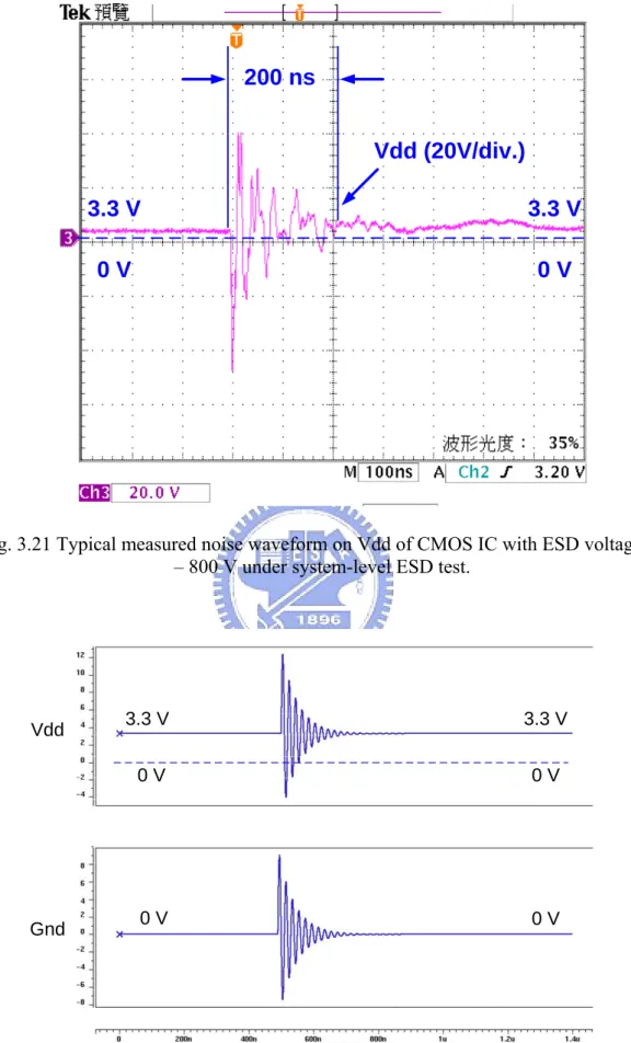
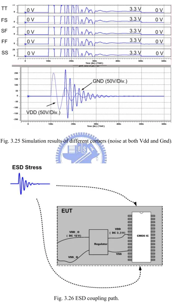
According to the waveform measured during ESD stress, which is shown in Fig. 3.21, the underdamped sine wave is adopted to simulate the noise of the detection circuit induced from ESD stress practically. The test waveform is shown in Fig. 3.22. In order to simulate the detection circuit with all kinds of noise on the power-line, underdamped sine waves with various frequency, amplitude, and delay time noises are applied on the power-line of the detection circuit. The simulation waveforms are shown in Figs. 3.23, 3.24, and 3.25. According to the waveform shown in Fig. 3.22, the period of the noise is about 300ns. (The
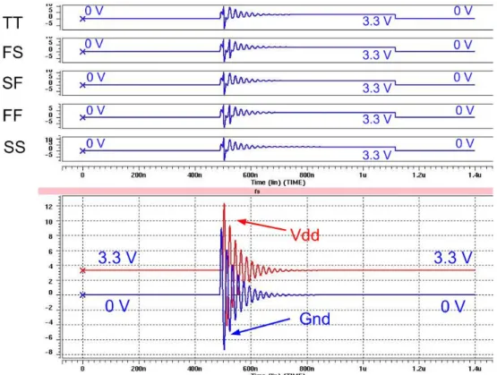
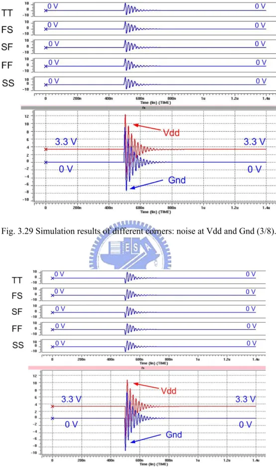
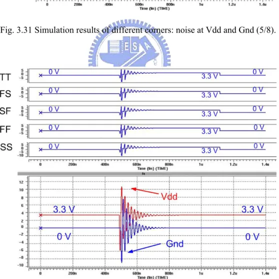
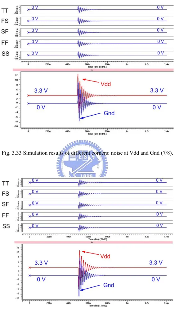
frequency of the noise is about 40MHz). The amplitude of the noise is selected ranging from 1/2 Vdd to hundreds of voltage. The ESD stress will affect the system in varies way, which is shown in Fig. 3.26. Therefore, this situation can be studied by simulation with different delay time between noise at Vdd and Gnd. The simulation results are shown in Figs. 3.27 to 3.34. As a result, when the delay time between the noises on Vdd and Gnd is more than 10 ns, the output state of the transient detection circuit will be changed. When the delay time between the noises on Vdd and Gnd is less than 3ns, the output states of the transient detection circuit will not be changed. .
As the simulated result shown, the parasitic diode will be turned on if the voltage between Vdd and Gnd is less than the threshold of the MOS. The output state of the transient detection circuit will be changed when the power of the detection circuit returns to its normal voltage.
3.4 C
ONCLUSIONTo investigate the physical mechanism of detection circuit under system-level ESD test, underdamped sine waves with various frequency, amplitude, and delay time noises are applied on the power line of the detection circuit. Some simulation results can be demonstrated under simple peak noise on power line of IC. Therefore, the detection circuit will be verified under system-level ESD test, and the measurement results will be shown in next chapter.
Reset_N
Q
Sensor_2 Sensor_1
Fig. 3.1 Convention circuit diagram of ESD sensor.
VDD tr/tf=1ns tr/tf=1ns tr/tf=10ns tr/tf=10ns Vp=-1.2V Vp=0V Q=0 Q=1
Fig. 3.2 Simulation result of the ESD sensor (noise at Vdd).
tr/tf=1ns tr/tf=1ns tr/tf=10ns tr/tf=10ns Vp=6.2V Vp=5V Q=0 Q=1 VSS
Fig. 3.4 Circuit diagram of detection circuit (NMOS).
Fig. 3.6 Simulated result of detection circuit (1).
Fig. 3.7 Simulated result of detection circuit (2) (Vdd).
Fig. 3.9 Simulation results of different noise peak of Vdd (Q = 6).
1 2 3 4 5 6 2.0 2.1 2.2 2.3 2.4 2.5 N o ise Peak o f Vd d (V) Q
Fig. 3.11 Noise peak of Vdd vs. parameter Q (1/2).
0.0 0.2 0.4 0.6 0.8 1.0 1.2 2.80 2.85 2.90 2.95 3.00 3.05 No ise Peak o f Vdd (V) Q
Fig. 3.13 Simulation results of different noise peak of Vdd (coupling capacitance: 0.1 pF).
0 1 2 3 4 5 2.3 2.4 2.5 2.6 2.7 2.8 2.9 No ise Peak of Vd d (V) Coupling Capacitance (pF)
Fig. 3.15 Noise peak of Vdd vs. coupling capacitance.
Fig. 3.17 Simulation waveforms of different noise peak of Gnd (Q=1/6). 1 2 3 4 5 6 2.0 2.1 2.2 2.3 2.4 2.5 N o ise Peak o f Gnd (V) Q
0.2 0.4 0.6 0.8 1.0 2.60 2.65 2.70 2.75 2.80 Noi se Peak o f Gnd (V) Q
Fig. 3.19 Noise peak of Gnd vs. parameter Q (2/2).
0.0 0.5 1.0 1.5 2.0 2.5 3.0 2.3 2.4 2.5 2.6 2.7 2.8 2.9 N o ise Peak o f Gnd (V) Coupling Capacitance (pF)
Vdd (20V/div.)
0 V
3.3 V
0 V
3.3 V
200 ns
Fig. 3.21 Typical measured noise waveform on Vdd of CMOS IC with ESD voltage of – 800 V under system-level ESD test.
3.3 V 3.3 V
0 V 0 V
0 V 0 V
Vdd
Gnd
Fig. 3.22 Underdamped sine wave voltage used in HSPICE to simulated the noise voltage under system-level ESD test.
Fig. 3.23 Simulation results of different corners (noise at Vdd).
Fig. 3.25 Simulation results of different corners (noise at both Vdd and Gnd).
Fig. 3.27 Simulation results of different corners: noise at Vdd and Gnd (1/8).
Fig. 3.29 Simulation results of different corners: noise at Vdd and Gnd (3/8).
Fig. 3.31 Simulation results of different corners: noise at Vdd and Gnd (5/8).
Fig. 3.33 Simulation results of different corners: noise at Vdd and Gnd (7/8).
C
HAPTER
4
M
EASUREMENT
In order to evaluate the performance of electrical/electronic equipments when subjected to ESD events, performing the system-level ESD test for the electrical/electronic equipments is necessary. Electrostatic discharge (ESD) is a high-amplitude event that causes permanent damage, latent failures, or disruption in functional operation. Performing an ESD test is a powerful method of determining potential failures over an extremely wide spectrum of frequencies. When applied in a conducted manner, this pulse creates an extremely strong electromagnetic field. Compared to the electrical fast transient (EFT) test, which essentially excites cables, ESD also evaluates box shielding and PCB layout deficiencies as well as manifests currents in cables.
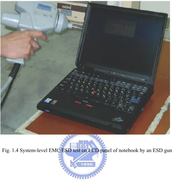
4.1 M
EASUREMENTS
ETUPA notebook under the system-level ESD test with direct contact-discharge test mode is shown in Fig. 1.4. An electrical/electronic product with CMOS ICs must sustain the ESD level of ±8 kV under contact-discharge test mode to achieve the immunity requirement of “level 4” in the system-level ESD test, which is shown in table 2.2. The product must sustain the ESD level of ±15 kV under air-discharge test mode to achieve the same requirement. During such a system-level ESD test, electromagnetic interference (EMI) coming from the ESD stress will be coupled into the driver ICs of the liquid crystal display (LCD) panel. The ESD-generated transient voltage is quite large (with an amplitude of several tens to hundreds of volts) and fast