國 立 交 通 大 學
電子工程學系 電子研究所碩士班
碩 士 論 文
懸浮式奈米線通道電晶體於氣體感測器之應用
與具懸浮式閘極之垂直電晶體特性研究
A Study on Gas Sensor Applications of
Suspended-Nanowire-Channel TFTs and the
Characterization of Suspended-Gate
Vertical-MOSFETs
研 究 生:王崇名
指導教授:林鴻志 博士
黃調元 博士
中
華 民 國 一○○ 年 七 月
懸浮式奈米線通道電晶體於氣體感測器之應用
與具懸浮式閘極之垂直電晶體特性研究
A Study on Gas Sensor Applications of
Suspended-Nanowire-Channel TFTs and the
Characterization of Suspended-Gate
Vertical-MOSFETs
研 究 生:王崇名 Student: Chung-Ming Wang
指導教授:林鴻志 博士 Advisors: Dr. Horng-Chih Lin
指導教授:
黃調元 博士
Dr. Tiao-Yuan Huang
國 立 交 通 大 學
電子工程學系 電子研究所碩士班
碩 士 論 文
A Thesis
Submitted to Department of Electronics Engineering & Institute of Electronics College of Electrical and Computer Engineering
National Chiao-Tung University in Partial Fulfillment of the Requirements
for the Degree of Master of Science
in
Electronics Engineering July 2011
Hsinchu, Taiwan, Republic of China
懸浮式奈米線通道電晶體於氣體感測器之應用
與具懸浮式閘極之垂直電晶體特性研究
研究生:王崇名 指導教授:林鴻志 博士
黃調元 博士
國立交通大學
電子工程學系 電子研究所碩士班
摘要
在本篇論文中,我們成功地製作出兩種新穎的元件結構,分別為懸浮式奈 米線通道電晶體及具懸浮式閘極之垂直電晶體。其中,前者的懸浮式奈米線通 道、與後者的懸浮式閘極電極及垂直通道皆利用一簡單且低成本的非等向性電漿 蝕刻技術來完成。 首先,我們成功地將懸浮式奈米線通道電晶體用應用於氣體感測器。在含氨 氣的環境中,懸浮式奈米線通道電晶體的基本電性會隨著氨氣的濃度而有所反 應。我們可以藉由觀測汲極電流(ID)和啟動電壓(Vth)隨著氨氣濃度的變化,來偵 測氨氣的濃度,並且分析氨氣在奈米線表面的反應機制。另外,我們藉由改變懸 浮式閘極電晶體元件光罩的設計,成功地改善了兩段式啟動現象,並且探討該元 件改善後的基本電性。最後我們移除犧牲氧化層,且成功地使閘極電極懸浮於空 氣中。
A Study on Gas Sensor Applications of
Suspended-Nanowire-Channel TFTs and the
Characterization of Suspended-Gate
Vertical-MOSFETs
Student: Chung-Ming Wang Advisors: Dr. Horng-Chih Lin
Dr. Tiao-Yuan Huang
Department of Electronics Engineering and Institute of Electronics
National Chiao Tung University, Hsinchu, Taiwan
Abstract
In this thesis, we have successfully fabricated two kinds of devices including the suspended-NW-channel TFTs and the SG vertical-MOSFETs. The sidewall spacer NW in suspended-NW-channel TFTs and the sidewall spacer gate electrode in the vertical channel of SG vertical-MOSFETs are both formed by a simple anisotropic plasma etching technique.
We have successfully applied the suspended-NW-channel TFT to gas sensor application. In the environments containing ammonia (NH3), the basic electrical characteristics of the suspended-NW-channel TFT are changed with the variation in the concentration of NH3. The shift in threshold voltage (Vth)or the change of drain current (ID) with varying NH3 concentration can be used as an indicator to sense the
surface are discussed and analyzed. Besides, we have also successfully improved the undesirable two-step turn-on phenomenon encountered in the characterization of SG vertical-MOSFETs conducted in a previous work by changing the mask layout, and studied the basic electrical characteristics of the newly designed and fabricated SG vertical-MOSFETs. Finally, we have successfully removed the sacrificial oxide layer to suspend the side gate and studied the characteristics of the devices.
Acknowledgment
民國一百年,這個獨具紀念價值的一年,也是我學生生涯的最後一年。雖說 是脫離了學生身分,但是世界之大,做為學生時期所學的是不夠的,還有更多做 人處事的道理以及知識才是往後需要繼續學習的課題。 在交大兩年的時光中,首先要特別感謝兩位指導教授 林鴻志 教授以及黃 調元 教授。由於兩位老師對於教學有著一定的堅持與熱誠,我才能從中有所收 穫與成長。尤其是擔任黃老師課程助教期間,讓我學會面對問題時所應當具備的 處理態度,更應該設身處地地替他人著想。在這裡非常謝謝兩位老師,謝謝你們 的指教。 當然,還有ADTL 的各位都是我最珍貴的朋友。特別要先感謝郭嘉豪學長, 感謝學長一路帶我做實驗,幫忙我解決實驗上的問題,還有在量測及結果的分析 上,也都給了我很大的幫助。再來還要感謝林哲民學長、陳威臣學長、徐行徽學 長、蔡子儀學長、林政頤學長、李克慧學姐,在我不知所措時適時的給我意見及 方向。還有同樣一起奮鬥兩年的同伴們,大鳥(吳俊鵬)、林歷樺、顏博士(顏同偉)、 亞洲潮男(許宇賢)、Wada(蘇段凱)、交大濕男(卞孝雄),當然還有鍾嘉文,感謝你 們給我這麼多的歡樂,認識你們真好。當然,還有一群吵鬧的學弟妹,讓我的研 究生涯更加歡樂。我就先出海了,我要成為海賊王! 還要特別感謝負責量測儀器的羅淵仁學長、季維康及陳瑞然,幫助我解決量 測時所發生的問題。 另外,還要感謝這一路上我所有的好朋友、好兄弟、好姊妹,讓我在放假的 時候可以打打嘴砲,一點也都不無聊。雖然現在大家都在不同的地方發展,但是 你/妳們永遠都是我的好朋友,因為我們是夥伴啊(×)! 最後,最要感謝的是我的爹娘,沒有你們就沒有現在的我。老爹我知道平常 你話很少,但是都有在默默的關心我,所以你也要照顧好自己的身體,不要再抽 菸了,不管你是用吃的還是用吸的都一樣。還有老媽,我真的不是只有沒錢才會 打電話回家,我都有默默的關心妳跟老爹。差點忘了還有老姊,妳真的是個好姊 姊,好到可以出國比賽了。在這個時刻,也希望你們會因我而感到無比驕傲,也 是因為你們,才讓我有繼續向前走的動力。最後是米恩、米魯,你們這兩隻笨狗 不要再給我隨地大小便了! 謹獻給所有幫助我、鼓勵我,以及所有我所敬重、珍惜的師長、朋友們。感 謝你/妳們。 王崇名 誌於 風城交大 2011 年 7 月Contents
Abstract (Chinese)……… i
Abstract (English)……… ii
Acknowledgment (Chinese)……… iv
Contents……… v
List of Figure Captions……… vii
List of Table Captions……… xi
Chapter 1 Introduction………..
11.1 Overview of the Gas Sensor………... 1
1.1.1 Solid Electrolyte Gas Sensors………..…… 2
1.1.2 Catalytic Gas Sensors………...…... 3
1.1.3Semiconductor Oxide Sensors……….…… 4
1.2 Application of Metal-Oxide-Semiconductor Field-Effect-Transistors for Gas Sensing. 5 1.2.1 Suspended-Gate MOSFET (SG-MOSFET ) ………...…… 7
1.2.2 Suspended-Nanowire (NW)-Channel Device……….. 8
1.3 Motivation………... 8
1.4 Organization of this Thesis………...……….. 9
Chapter 2 Device Structure and Fabrication………..
122.1 Device Structure and Process Flow of Suspended-NW-Channel TFTs……….. 12
2.2 Device Structure and Process Flow of SG Vertical-MOSFETs……….. 13
2.3.1 Measurement Setup of Basic Electrical Characteristics……….. 15
2.3.2 Measurement Setup of Gas Sensor……….. 16
Chapter 3 Results and Discussion……… 17
3.1 Basic Characteristics of Suspended-NW-Channel TFTs……… 17
3.1.1 Hysteresis Phenomenon………... 18
3.1.2 Hydrogen Passivation Effects……….. 18
3.2 Suspended-NW-Channel TFTs for Gas Sensor Applications………. 21
3.2.1 NH3 Passivation Effect………. 22
3.2.2 Sensing Limit………... 23
3.2.3 Relationship between Air Gap and Sensibility……… 23
3-3 Basic Characteristics of SG Vertical-MOSFET……….. 24
Chapter 4 Conclusion……… 29
References……… 31
Figure Captions……… 34
Vita……… 66
List of Figure Captions
Chapter 1
Fig. 1.1. Schematic structure of equilibrium-potential-type oxygen sensor [6]. …… 34 Fig. 1.2. Schematic structure of limiting current type oxygen sensor [7]. …………. 35 Fig. 1.3. Current-voltage characteristics of a limiting-current-type oxygen sensor
[7]. ……… 35
Fig. 1.4. Schematic diagram of Catalytic gas sensor [6]. ………... 36 Fig. 1.5. Cross-sectional-view of an n-MOSFET. ……….. 37 Fig. 1.6. Energy band diagram of an MOS capacitor. (a) Gate bias is zero. (b) Gate
bias is equal to threshold voltage. ………... 37 Fig. 1.7. Typical 3D structure of a SG-MOSFET [12]. ……….. 38 Fig. 1.8. An equivalent electrical circuit of SG-MOSFET [13]. ……… 38 Fig. 1.9. The operation principle of SG-MOSFET. The mobile gate is controlled by
electrostatic force and elastic force [12]. ………. 39 Fig. 1.10. The operation principle of SG-MOSFET. (a) Gate bias is smaller than
pull-in voltage. (b) Gate bias is equal to pull-in voltage [12]. ………. 39 Fig. 1.11. Transfer characteristics of SG-MOSFET, showing the hysteresis
phenomenon [13]. ……… 40 Fig. 1.12. Stereo view and cross-sectional view of the suspended-NW-Channel TFT
[14]. ……….. 41 Fig. 1.13. Transfer characteristics of suspended-NW-Channel TFT, showing the
hysteresis phenomenon [14]. ………... 41
Chapter 2
Fig. 2.1. The structure and process flow of the suspended-NW-channel TFT. (a) Top-view of the suspended-NW-channel TFT. (b) Patterned gate electrode consisted of an in-situ doped n+ poly-Si. (c) Deposition of silicon nitride
dielectric, sacrificial layer and amorphous Si. (d) Fabrication of S/D regions and sidewall spacer NW-channel by plasma etching. (e) Photoresist capping of the channel region and S/D implantation. (f)
Removal of the sacrificial layer to form the suspended NW-channels. …... 42 Fig. 2.2. The structure and process flow of the SG vertical-MOSFET. (a) Top-view
of the SG vertical-MOSFET. (b) Definition of the S/D areas and vertical channel regions, and growth of a screen oxide. (c) Deposition of buffer oxide, silicon nitride dielectric, sacrificial layer and in-situ doped n+ poly-Si gate. (d) Definition of gate area and sidewall spacer gate electrodes by plasma etching. (e) Removal of the TEOS oxide capping on S/D areas and S/D implantation. (f) Removal of the sacrificial layer to form the suspended gate electrode. ……….. 43 Fig. 2.3. Cross-sectional TEM images of a fabricated SG vertical-MOSFET along
the dotted line AB in Fig. 2.2(a) with different vertical channel length. (a) 1 μm. (b) 0.5 μm. ……… 44 Fig. 2.4. Schematic diagram of the gas sensing measurement system. ……….. 45
Chapter 3
Fig. 3.1. Transfer characteristics of (a) conventional NW-channel TFT and (b)
suspended-NW-channel TFT. ……….. 46
Fig. 3.2. Fresh transfer characteristics of a suspended-NW-channel TFT. ………… 47 Fig. 3.3. The motion of the NW being swayed by forward and reverse sweeping
measurments. (a) The NW is suspended, i.e., Fe<Fk. (b) The NW is pulled-in and touches the side gate, turning on the device, i.e., Fe>Fk. (c) The NW channel region is fully attached to the side gate. (d) The attached NW is about to be released from the side gate, i.e., Fe+Fv<Fk. (e) The NW is fully released and return to the suspended state. ……….. 47 Fig. 3.4. Transfer characteristics of suspended-NW-channel TFT measured in
atmosphere and vacuum. ……….. 48 Fig. 3.5. Schematic diagram of poly-silicon grain boundary. (a) Hydrogen
passivation on defects at fresh state. (b) At vacuum state, the passivated hydrogen is pulled out from grain boundary. (c) After returning to atmosphere, hydrogen species return to grain boundary near the NW surface, and form a shield to hinder further hydrogen in-diffusion, preventing fast re-passivation in the NW core. ……… 49 Fig. 3.6. The hydrogen de-passivation effect with typical-NW-channel TFT and 50
suspended-NW-channel TFT. ……….. Fig. 3.7. Transfer characteristics of suspended-NW-channel TFT with H2 sinter
treatment. ………... 50 Fig. 3.8. Transfer characteristics of a suspended-NW-channel TFT with air gap of
20 nm, measured in environments with various NH3 concentrations. …….. 51 Fig. 3.9. Shift in threshold voltage vs. NH3 concentration. ………. 51 Fig. 3.10. Subthreshold swing vs. NH3 concentration. ……….. 52 Fig. 3.11. Transfer characteristics of a suspended-NW-channel TFT with air gap of
85 nm, measured in environments with various NH3 concentrations. …….. 53 Fig. 3.12. Shift in threshold voltage vs. NH3 concentration. ………. 53 Fig. 3.13. Real-time drain current measurement of a suspended-NW-channel TFT. … 54 Fig. 3.14. Relative conductance as a function of NH3 concentration presenting in the
test environment. ……….. 55 Fig. 3.15. Band diagrams of the suspended-NW-channel TFT with air gap of 20nm
and 85 nm. (a) In the fresh state. (b) Enhanced surface band bending after
NH3 is introduced. ………. 56
Fig. 3.16. Schematic configurations of (a) A and (b) B modes of operation. ………... 57 Fig. 3.17. (a) Schematic cross-sectional view of the SG vertical-MOSFET in which
the vertical channel length and horizontal channel length are defined. (b) TEM image of a device fabricated on wafer #2 in Table 1. ……….. 58 Fig. 3.18. Typical transfer characteristics of SG vertical-MOSFET devices measured
under A mode of operation, fabricated with (a) original [15] and (b) revised layouts. ……….. 59 Fig. 3.19. Transfer characteristics of SG vertical-MOSFETs under A operation mode
(a) without sacrifice oxide and (b) with sacrificial oxide of 50 nm…. 60 Fig. 3.20. DIBL as a function of the total channel length (Ltotal) for devices with
various sacrificial oxide thickness. ………... 61 Fig. 3.21. Threshold voltage (Vth) as a function of the total channel length (Ltotal) for
devices with various sacrificial oxide thickness. ……….. 61 Fig. 3.22. Subthreshold swing (SS) as a function of the total channel length (Ltotal) for
devices with various sacrificial oxide thickness. ………. 62 Fig. 3.23. Output characteristics of the SG vertical-MOSFETs operated under A
mode with vertical channel length (LCv)of (a) 0.3 μm, (b) 0.5 μm and (c) 1
μm. ………. 63
Fig. 3.24. Transfer characteristics for a device without sacrificial oxide operated
under A and B modes. ……… 64
Fig. 3.25. Output characteristics of a device without sacrificial oxide operated under
A and B modes of operation. ……….. 64
Fig. 3.26. Hysteresis transfer characteristics of a SG vertical-MOSFET with air gap of 100 nm. ………. 65
List of Table Captions
Chapter 1
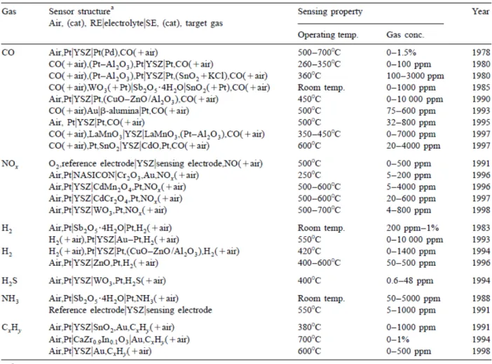
Table 1.1. Typical examples of mixed-potential-type gas sensors [8]. ………. 11
Chapter 3
Table 3.1. Structural parameters for the SG vertical-MOSFETs. ………. 28 Table 3.2. The mean value of Vth, DIBL and SS extracted from SG
Chapter 1
Introduction
1.1 Overview of Gas Sensor
In recent years, optic spectra of atom and molecule are used to decipher different gas substance [1]. This method has very high accuracy. However, the analysis equipment is not universally applied in general living because of the complexity, large volume and expensive cost.
Nowadays there are increasing worldwide requirements for gas sensors with low power, low cost, high sensitivity and high selectivity. The detectors are in demand for sensing toxic gases in order to protect people’s life and safety. In practice, gas detectors have also been widely applied in the manufacturing environment of advanced semiconductor industry. Ever since the first patent of gas sensor in the world by James W. Johnson on Jan. 16, 1923 [2], research and development of gas detector technology had been thriving in both academia and industry. Many different kinds of gas detectors were proposed and developed, such as galvanic-system-based gas sensor [3], solid electrolyte sensor [4] and semiconductor gas sensor, [5] etc.
Solid state gas sensors had been booming in late 20th century. Key components of this kind of gas sensors available in the market are solid state devices. Because of the minor device volume and simple construction process, solid state gas sensors are attractive and can be easily integrated in a variety of operation systems. Principle working mechanisms are mainly related to the chemical reactions or physical processes taking place on detector surface. Occurrence of the surface reactions is
transferred into mainly electrical signals through the sensing. Nonetheless, details about the mechanisms of gas sensing are very complicated and multidisciplinary in nature, including electronics, chemistry, physical and materials science.
1.1.1 Solid Electrolyte Gas Sensors
Solid electrolyte sensor is a valuable technique because it has high sensitivity and high selectivity. It has been widely applied to auto industry, green industry and many different areas. According to the principles of operation, there are three sub-divisions of solid electrolyte sensors, namely, equilibrium potential type, limiting-current type and mixed potential type.
Fig. 1.1 [6] is an example for equilibrium-potential-type oxygen sensor which uses a reference gas as the baseline. The cathode and anode of the sensor are put into the reference gas and test gas, respectively. The electrodes of the sensor produce a potential difference due to the different gas partial pressures and we can measure the test gas partial pressures via the Nernst equation.
) ln( 4 t r P P F RT V = , (Eq.1-1) where R is the gas constant, T is the temperature, F is Faraday constant, Pr is partial pressure of reference gas and Pt is partial pressure of test gas.
Gas sensors of the limiting-current type detect the gas concentration through sensing the ion current. First, a constant voltage is applied to the device and the purpose is to promote the chemical reactions. Fig. 1.2 [7] shows the structure of a limiting-current-type oxygen sensor. The oxygen is reacted and generates O2--ions at cathode and then ions flow into the anode by solid electrolyte. Moreover, the reaction rate of O2--ions is proportional to the applied voltage. Fig. 1.3 [7] is the
current-voltage characteristics of a limiting-current-type oxygen sensor. The relationship between voltage and ion current follows Ohm’s law when the voltage is small. However, after the applied voltage reaches a limiting value, the generation rate of O2--ions is higher than the mobility of ions. Then the ion current will tend to saturate and this saturation current has a positive ratio with gas concentration.
Sensing principle of mixed-potential-type gas sensors are the most complex among the solid electrolyte sensors. More than one chemical reactions take place at the electrodes and complicate the detection of the electrochemical potential. However, we can directly sense a specific kind of gas in a specific range of gas concentration by combination of different electrolyte and electrode materials. Table 1 [8] shows typical examples of mixed-potential-type gas sensors. While the mixed-potential-type gas sensor is more complicated than other types of techniques, it has better sensing response and high selectivity.
1.1.2 Catalytic Gas Sensors
Catalytic sensors are usually applied to monitor flammable and potential explosive mixtures of gases, such as methane, butane, hydrogen, and so on. It helps us to manage the dangerous environments and protect our life and property. However, the most important matter is to prevent the explosion from occurring rather than what kind of gases are contained in the environment. Therefore, the sensitivity is more important than the selectivity for catalytic gas sensors.
Fig. 1.4 [6] is schematic diagram of a catalytic gas sensor. This sensor is a combination of two kinds of devices, a sensing device and a reference device. The sensing device is a resistance-type detector and usually a heating wire having texture made of precious materials. However, burning of flammable gas would take place
when undergo exothermic reaction through heating or reacting with catalytic. The resistance of the heating wire tends to increase as the flammable gas is burned to raise the temperature of the sensing device. In addition, the reference device is not sensitive to the flammable gas. Therefore, we can detect the gas concentration by comparing the difference in resistance between the sensing and reference devices.
1.1.3 Semiconductor Oxide Sensors
In 1953, P. B. Weisz proposed that semiconductor can be applied for the application of gas sensors at temperature in the range of 300-500℃ because the resistance of a semiconductor material can be manipulated by the adsorption of gas molecule on the semiconductor surface. Thus semiconductor oxide sensors are mainly a member of resistance-type detectors. Examples of popular materials include TiO2,
Ga2O3, WO3, BaSnO3, and so on. The semiconductor oxide can be classified into
n-type or p-type, depending on whether the major carrier is electron or hole, respectively.
We can divide sensing mechanism of semiconductor oxide detectors into two types, namely, the bulk type and surface type. In general, the relationship between conductivity and partial pressure of test gas can be expressed by
) 1 ( ) ( N t kT E P Ae A − = σ , (Eq.1-2)
where σ is the conductivity, A is a constant, EA is the activation energy, and N is a constant determined by the dominant type of bulk defects [6]. When gas molecules are adsorbed on the surface, catalytic combustion would occur. With oxygen as an example,
2
2 4 2
It may snatch electrons from valence band of the semiconductor and increase the hole concentration for p-type semiconductor or release electrons to the conduction band to increase the electron concentration. Through the surface effects, the semiconductor oxide resistance is modulated.
1.2 Application of Metal-Oxide-Semiconductor
Field-Effect-Transistors for Gas Sensing
The transistor can be arguably called one of the greatest inventions in the 20th century. In 1947, Bardeen, Brattain and Shockley demonstrated the first solid-state triode showing amplification effect of current at Bell Lab in USA, and they named the device “Transistor”. Compared with the vacuum tube, the transistor has the advantages of small volume, low power consumption and quick response. Therefore, vacuum tubes were quickly replaced by transistors in related applications. So far, transistors had been developed for over half a century. With the drastic advancement made in device density and operation speed, we can now enjoy a number of convenient electronic products such as mobile phone, portable computers, memory cards and various types of detectors.
Fig. 1.5 shows the cross-sectional view of an n-type metal-oxide-semiconductor field effect transistor (MOSFET) which is formed on a p-type silicon wafer and has heavily-doped n-type source/drain terminals. Moreover, silicon dioxide (SiO2) and
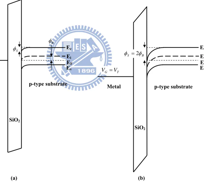
metal are treated as gate insulation and gate electrode, respectively. The structure and function of a transistor resembles a water-tap for controlling water flow. That is, the gate electrode acts likes a switch to control the electron flow from the source end to the drain end. Fig. 1.6 shows the energy band diagram of a p-MOS capacitor. When
two different materials are linked together, at thermal equilibrium, their Fermi levels would be adjusted to be the same. Therefore, the energy band bending is taken place in the p-type substrate near the insulation/substrate interface, as shown in Fig. 1.6(a). The amount of energy band bending in silicon is called the surface potential (φS). When we apply a positive gate bias and increase it gradually, surface potential will be increased. In Fig. 1.6(b), the surface potential is two times of φ , i.e., the difference B
between the Fermi energy and intrinsic energy. At this stage a strong inversion is induced at the p-type substrate surface and the transistor is defined to be “turned on” and the gate voltage is called the threshold voltage (Vth) [9]. Vth can be expressed with the form: ox dep ox ox MS B th C Q C Q V =2φ +φ − + , (Eq.1-4) where φMS is the work function difference between metal and silicon substrate, Cox is
the capacitance of gate oxide, Qox is the charge in gate oxide and Qdep is the charge in the depletion layer of substrate.
MOSFET gas sensor was applied to detect hydrogen from the earliest stage [6][10]. In the operation hydrogen is adsorbed at the surface of gate metal and reaches the interface between metal and gate insulator through metal layer by diffusion. Usually the MOSFET has to be heated to promote the hydrogen diffusion. Take n-MOSFET as an example, passivation of the hydrogen at the metal/gate insulator interface will increase the surface potential and decreases the Vth. The hydrogen concentration can thus be determined by the shift in Vth. In addition, we can also stack a sensing layer in contact with the gases to be sensed. This way is useful for increasing the selectivity and sensitivity. Based on the material option, the sensing layer can be divided into metals, semiconducting metal oxides, hydrated salts, polymers and organics [11].
1.2.1 Suspended-Gate MOSFET (SG-MOSFET )
Fig. 1.7 [12] and Fig. 1.8 [13] show the typical 3D structure and equivalent electrical circuit of a SG-MOSFET, respectively. The major difference between traditional MOSFET and SG-MOSFET is that there exists an air gap between the suspended gate (SG) and gate oxide layer. In other words, the SG is just like a suspension bridge. Because of the lower dielectric constant of air gap, there is a large effective oxide thickness (EOT). SG-MOSFET has a low gate leakage current as the transistor is operated at the off state. When used as a gas sensor, the operation mechanisms are different from those of the previous MOSFET gas sensors in that the diffusion of the gas molecules in the gate is not necessary. Finally, SG-MOSFET has a great potential for applications on memory devices and gas sensors.
Fig. 1.9 [12] shows the operation principles of the SG-MOSFET. For an n-type SG-MOSFET, when we apply a positive gate bias and increase it gradually, the positive charge is accumulated in the gate electrode. Similarly, the negative charge is also induced on the substrate surface for charge neutrality. Because these positive and negative charges are attracted to etch other, the SG slowly approaches the substrate by the electrostatic force, as show in Fig. 1.10(a) [12], while there exists an opposite elastic force imposed on the SG to balance the electrostatic force. As the gate bias further increases, eventually the electrostatic force would be sufficiently large to force the SG to contact with the gate oxide, as shown in Fig. 1.10(b) [12]. During the switching process the air gap thickness would change and therefore the EOT of the device is not a constant but a function of the gate voltage. When the pull-in action of the SG occurs, a steep transfer characteristic shown in Fig. 1.11 can be observed [13]. The corresponding gate bias is called the pull-in voltage (Vpi). Conversely, during the reverse sweeping the SG would separate from the gate oxide at a gate bias called the
pull-out voltage (Vpo). Since there exists an additional surface adhesion force between the SG and gate oxide when they are in contact, Vpo is smaller than Vpi, leading to the hysteresis phenomenon in the transfer characteristics, as shown in Fig. 1.11 [13].
1.2.2 Suspended-Nanowire (NW)-Channel Device
Our group recently proposed an alternative structure featuring suspended NW Channels [14]. The manufacturing process is simple and does not rely on advanced lithography technology. Fig. 1.12 [14] shows the stereo and cross-sectional views of the suspended-NW-Channel thin film transistor (TFT). We can easily reduce the sacrificial oxide thickness to below 100 nm and use wet etching to remove it. As a result, sub-100 nm air gap can be formed easily.
The operation principles of the suspended-NW-Channel TFT is similar to that of the SG-MOSFET stated above. As the gate is applied with a sweeping voltage, the suspended NW channel is swung by the electrostatic force and elastic force. We can thus observe a hysteresis phenomenon like SG-MOSFET, as shown in Fig. 1.13 [14].
1.3 Motivation
In the past decades, great advancement in science and technology has significantly changed the civilization of human and brought a lot of convenience in our daily life. Nonetheless, a lot of harmful exhaust gases have also been generated and are polluting our atmosphere. Monitoring of the harmful exhaust gases in some specific locations, such as the working environment of a manufacturing plant, has thus become an important and urgent need. Through the narrative given in Sections 1.1 and
1.2, we can understand that most of the gas sensors require heating to catalyze the required chemical reactions between the sensing material and gases, and provide the gas species to be detected with enough kinetic energy to diffuse. However, the detector has to operate around-the-clock to provide human with enough protection. It is quite certain that the heating would consume a great amount of power. Such an issue can be addressed with the suspended device which exhibits low leakage current and do not rely on the heating in practical applications.
In prior study [15], our group had studied two kinds of MOSFET equipped with a suspended gate or channel and explored their feasibility for gas sensing applications. However, that previous study did not investigate the response of the devices to the concentration of the detection species. In this thesis, we intend to explore and understand the sensing limit of those devices with suspended objects. Moreover, the performance of the SG vertical-MOSFETs proposed and demonstrated in the previous work was unsatisfactory, and has been identified to be related to the inappropriate mask design. This also motivates us to design a new set of masks to fabricate and achieve improved device characteristics.
1.4 Organization of this Thesis
In Chapter 2, we present the fabrication of the suspended-NW-channel TFT and SG VMOSFET. Basic process flows are briefly described. The measurement setups are also presented in this chapter.
In Chapter 3, we present and discuss the electrical characteristics of the fabricated devices tested in different environments, including atmosphere, vacuum and ammonia. The results of the suspended-NW-channel TFT and SG VMOSFET
will be discussed respectively.
Finally, we summarize the major conclusions from our experimental results in Chapter 4.
Table Captions
Table 1.1 Typical examples of mixed-potential-type gas sensors [8].Chapter 2
Device Structure and Fabrication
2.1 Device Structure and Process Flow of
Suspended-NW-Channel TFTs
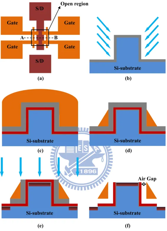
Fig. 2.1 shows the structure and process flow of the suspended-NW-channel TFT. Fig. 2.1(a) shows the top view of the device and the device key fabrication process flow is shown in Figs. 2.1(b)~(f) which illustrate the cross-sectional views at various steps along the dotted line AB in Fig. 2.1(a).
The fabrication began on a 6-in Si substrate capped with a 1000-nm thermal oxide layer. First, a 150nm-thick in-situ doped n+ poly-Si was deposited by low pressure chemical vapor deposition (LPCVD) at 550℃ and then patterned to form the gate electrode as show in Fig. 2.1(b). After the pre-furnace standard clean process, a 20-nm silicon nitride dielectric, sacrificial TEOS oxide layer and 150-nm amorphous Si were deposited in order. All these films were deposited by LPCVD at 780℃, 700℃ and 550℃, respectively. Besides, the sacrificial layer was split into 20-nm, 50-nm, and 80-nm in thickness to achieve different air gap thickness, as would become clear later. The amorphous Si was then re-crystallized to become polycrystalline in a furnace at 600℃ in N2 ambient for 24 hours, as shown in Fig. 2.1(c). The source/drain
(S/D) photoresist patterns were subsequently defined and an anisotropic plasma etching was performed to form the S/D simultaneously with the NW channels at the sidewall of the gates as shown in Fig. 2.1(d). Note that the dimension of the NW
channels can be controlled by the over etching time of the plasma etching. Subsequently, using another photoresist pattern to cap the channel region, an n-type S/D implant was conducted using P31+ at a dose of 5×1015 cm-2, as shown in Fig. 2.1(e). The dopant activation was simultaneously done with the deposition of a 500-nm TEOS oxide passivation layer deposited by LPCVD at 700℃. Finally, the contact holes were open by buffered oxide etchant (BOE) and hot 160℃ H3PO4 wet
etching process to remove the capping oxide and nitride over the electrodes, respectively. Here, a typical NW-channel TFT was completed.
To suspend the NW-channel, a photoresist pattern was formed to cap the device except the central channel region, as shown in Fig. 2.1(a). A BOE wet etching was used to remove the sacrificial TEOS oxide layer between the NW channel and the silicon nitride layer. After removing the photoresist, we put the wafer on a hot plate of 115℃ to desiccate the devices. The NW channels became suspended and exposed to the air after this step, as shown in Fig. 2.1(f).
2.2 Device Structure and Process Flow of SG
Vertical-MOSFETs
Fig. 2.2(a) shows the top view of the device and Figs. 2.2(b) to (f) show the device key fabrication process flow with cross-sectional views along the dotted line
AB in Fig. 2.2(a).
Briefly, 6-in n-type Si wafers, with resistivity between 2-7 Ω.cm, were used as the starting substrates of p-type SG vertical-MOSFETs. First, S/D photoresist patterns were formed with a photolithography process, and then an anisotropic plasma etching step was applied to define the vertical channel region. In this thesis, the vertical
channel length was split to 300-nm, 500-nm and 1000-nm by controlling the etching-time. To remove the damage resulted during the plasma etch, a 35-nm sacrificial thermal oxide was grown on the surface of the Si wafers. This oxide layer also serves as a screen oxide to avoid channeling effect in the next channel implantation step. A phosphorous ion implantation at 170 keV with a dose of 4×1012 cm-2 was used to dope the sidewall channel regions, and was carried out at a tilt angle of 45°, twist angle of 72° with the wafer rotated 4 times during implantation, as shown in Fig. 2.2(b). Afterwards, the sacrificial oxide was etched by a BOE wet etching. The RCA clean was applied before the sequential deposition of four films, as shown in Fig. 2.2(c). First, a 3-nm TEOS oxide was deposited by LPCVD at 700℃ to serve as a buffer layer. Second, a 20-nm silicon nitride was deposited by LPCVD at 780℃ as gate oxide layer. Third, a sacrificial TEOS oxide layer of 50-nm or 80-nm as a sacrificial layer. Finally, a 150nm-thick in-situ doped n+ poly-Si was deposited by LPCVD at 550℃ to serve as the material of gate electrode. Afterwards, a second mask was used to define the pad area of the gate. The gate pad and the sidewall spacer gate electrode were formed simultaneously with an anisotropic plasma etching step, as shown in Fig. 2.2(d). Next, a diluted hydrofluoric acid (DHF) wet etching was performed to etch the TEOS oxide layer capping on S/D area. Then BF249+ ions was
implanted to dope the S/D area at 25 keV with a dose of 5×1015 cm-2 and activated by rapid thermal annealing (RTA) at 1000℃, as shown in Fig. 2.2(e). And then a 400-nm passivation TEOS oxide layer was deposited to cap the entire wafer by plasma enhanced chemical vapor deposition (PECVD). Finally, we removed the top passivation layer, silicon nitride gate dielectric and TEOS oxide buffer layer by BOE, hot 160℃ H3PO4 and DHF, respectively, in order to open the contact holes. Here, a
Fig. 2.2(a).
The steps to suspend the sidewall spacer gate electrode are just like that described in Sec. 2.1. First, a photoresist mask was used to define the open region. Next, BOE and hot 160℃ H3PO4 wet etching were used to remove the sacrificial
layer and photoresist mask in order. Finally, the wet humidity remained on the wafer surface was removed by a hot plate set at 115℃. The resultant SG vertical-MOSFET is shows in Fig. 2.2(f).
2.3 Measurement Setup
2.3.1 Measurement Setup of Basic Electrical Characteristics
The basic I-V characteristics were measured by a precise measurement system including an HP 4156A precision semiconductor parameter analyzer, an Agilent TM 5250A switch and the Interactive Characterization Software (ICS) operating software at a stable environment at room temperature.
The basic electrical parameters of our device were extracted from the basic I-V characteristics. Due to the different operation behaviors exhibited by the two types of devices studied in this work, different definitions of threshold voltage (Vth) are necessary. Vth was defined as a value of gate voltage (VG) when the drain current (ID)
equals A under drain voltage (VD) was 0.1V for the
suspended- l TFTs, and L W ×10−9 NW-channe A L W ×10−7 under V D of -0.1V for the SG
vertical-MOSFETs, where W is the channel width and L is the channel length. The subthreshold swing (SS) was calculated by the following equation:
1 log − ⎟⎟ ⎠ ⎞ ⎜⎜ ⎝ ⎛ = G D dV I d SS . (Eq.2-1)
For both suspended-NW-channel TFT and SG vertical-MOSFET device, the average value of SS is considered.
2.3.2 Measurement Setup of Gas Sensor
In this study, the gas sensor measurements of all devices were evaluated by an airtight measurement system including a Keithley 4200 semiconductor characterization system, an ammonia source, a gas throttle, a flow controller, a vacuum pump and a closed chamber, as shown in Fig. 2.4.
The measurement system is capable of adjusting the ammonia concentration contained in the environments. In normal conditions, the environment is filled with fresh air in the closed chamber and the fresh-state I-V characteristics are recorded with the Keithley 4200 semiconductor characterization system. For gas sensing measurements, pure ammonia gas is introduced into the closed chamber. The ammonia concentration is controlled by the gas throttle and flow controller. According to a previous research, the diffusion coefficient of ammonia is 0.241 cm/s in nitrogen environment at atmospheric pressure and 20℃ [16]. So the measurements are conducted two minutes after the gas injection so that the ammonia could be uniformly distributed in the closed chamber. This scheme allows us to evaluate the response of the test device to the variation of ammonia content in the environment. The ammonia could be further injected to increase its concentration and repeated the measurements. The injection gases can be evacuated via a vacuum pump.
Chapter 3
Results and Discussion
3.1 Basic Characteristics of Suspended-NW-Channel
TFTs
Figs. 3.1(a) and (b) show the typical transfer characteristics of the conventional NW-channel TFTs and suspended-NW-channel TFTs, respectively. The difference in structure between the conventional and suspended-NW-channel TFTs is the existence of the air gap in the latter. The suspended-NW-channel TFT depicts a better subthreshold swing (SS) of 221 mV/dec as compared with a poorer SS of 627 mV/dec for the conventional one. Owing to the low dielectric constant of air, a nominal EOT of 341.73 nm for suspended-NW-channel TFT is actually much thicker than the EOT of 95.35 nm for the conventional NW-channel TFT. According to the relationship between SS and EOT:
⎟⎟ ⎠ ⎞ ⎜⎜ ⎝ ⎛ + = ox dep C C q kT SS 2.3 1 , (Eq.3-1)
where Cdep is depletion layer capacitance and Cox is the effective oxide capacitance, i.e., Cox∝ 1/EOT, the suspended-NW-channel TFT should has poorer SS, which is contrary to the observed trend. It can be attributed to the swaying of the NW channels. A detailed discussion about the operation mechanism is given later in Section 3.1.1.
3.1.1 Hysteresis Phenomenon
Fig. 3.2 shows the fresh transfer characteristics of a suspended-NW-channel TFT. The device exhibits a hysteresis phenomenon under forward and reverse sweeping measurments [11]. It is attributed to the motion of the NW being swayed by the electrosatic force (Fe) and elastic recovery force (Fk). Figs. 3.3(a) to (e) show the motion of the NW through forward and reverse sweeping measurments. First, Fe is very small when the device is in the off-state. The NW is suspended as shown in Fig. 3.3(a). At some momnet during the forward sweeping, Fe would become greater than
Fk and the NW is pulled toward and eventually touches the gate, as shown in Fig. 3.3(b). As the gate bias increases further, more channel regions are in contact with the gate, as shown in Fig. 3.3(c). On the other hand, during reverse sweeping the attached NW is released from the gate as the gate bias is sufficiently low. When the NW channels are in conatct with the gate nitride, the electrostic electric force is stronger than when they are apart due to the thinner EOT, while additional van der Waal force (Fv) is exerted (Fig. 3.3(d)). As a result, the pull-out action would occur at a gate bias lower than that of pull-in, leading to the hystersis characteristics. Finally, Fig. 3.3(e) shows the NW is pulled out from gate nitride and returns to suspensory status. Such mechanical pull-in and pull-out phenomena are depicted in Fig. 3.2. Owing to the fact that the NW-channel diameter is smaller than 100 nm, it is very soft. Sudden increase in drain current at VG=Vpi is not significant.
3.1.2 Hydrogen Passivation Effects
vacuum, and 80 minutes and 21 hours after returning to atmosphere. The air pressure is 0.2 torr for the vacuum state. It can be seen that SS dramatically increases from 223 mV/dec to infinite as the environment is switched from atmospheric to vacuum state. After returning to the atmosphere, the characteristics recover gradually and the SS is back to 235 mV/dec after 21 hours. This phenomenon can be ascribed to the passivation effect of water vapor [17][18]. Polycrystalline silicon is known to be granular in structure and contains a lot of grain boundaries at which many defects are located. Those defects are the root cause for mobility and SS degradation. Figs. 3.5(a) to (c) show the schematic diagram of poly-silicon grain boundaries. Generally, there exists an annealing procedure which introduces hydrogen-related species to decrease the amount of active defects and increase mobility of the polycrystalline silicon films. During the treatment, hydrogen species diffuse into polycrystalline silicon film and passivate the dangling bonds [18], as shown in Fig. 3.5(a). In vacuum state, the passivated hydrogen species are desorbed from polycrystalline silicon film and released into the environment, and leave the previously-passivated sites with the dangling bonds again. It is attributed to the reduction of chemical potential due to the decreasing pressure. The relationship between chemical potential and pressure of a perfect gas is [19] ln o o p RT p μ μ= + , (Eq.3-2) where μo and o
p are the chemical potential and pressure, respectively, at the standard state. The chemical potential in the gas is reduced when the pressure decreases to 0.2 torr. As a result, the hydrogen species tends to get expelled from grain boundaries to the vacuum. When the device is turned on, a large number of electrons are trapped in those defects, causing mobility degradation and reducing carrier concentration. Fig. 3.5(b) shows the schematic diagrams of hydrogen desorption from
the grain boundary. This explains why in Fig. 3.4 the drain current is too low to detect as the device is measured in vacuum. Fig. 3.6 compares the transfer characteristics of the NW devices with or without the air gap. Clearly the suspended-NW device has a much lower current. This is attributed to its larger area/volume ratio as compared with the conventional-NW device which has no air gap. In other words, desorption of the hydrogen species from the grain boundaries is expected to be more efficient in the suspended-NW device. Therefore, the hydrogen de-passivation effect of the suspended-NW is more evident than the conventional-NW device. As the environment returns to the atmosphere, hydrogen species contained in the environment may diffuse slowly back into the grain boundaries. Dangling bonds may be re-passivated by these returning hydrogen species, especially for those located closer to the NW surface. Nonetheless, the dangling bonds located in the NW core region would require a longer time to get re-passivated owing to the low environment temperature, as schematically shown in Fig. 3.5(c). Therefore, it may take a very long time to fully recover to the fresh state at room temperature. Fig. 3.7 shows the transfer characteristics of a suspended-NW-channel TFT measured at different environments or conditions, including the one with a forming gas (5% H2 in N2) sintering treatment
in a furnace at 400℃ for 30 minute. After the sintering treatment with a forming gas, the SS is 246 mV/dec, smaller than 338 mV/dec of the fresh state. This indicates the effectiveness of hydrogen passivation of the defects, and provides an indirect evidence for the above de-passivation effect used for explaining the experimental observations.
3.2 Suspended-NW-Channel TFTs for Gas Sensor
Applications
At first, the NH3 concentration in the measurement system is calculated. We have introduced this system in Section 2.3.2 and the system configuration is shown in Fig. 2.4. The ideal gas law will be considered as:
nRT
PV = , (Eq.3-3) where P is pressure, V is volume, n is the number (usually in moles) of gas molecules presenting in the system, R is the universal gas constant and T is the temperature [20]. In this study, in normal situations the pressure is controlled at 1 atmosphere, the volume of closed chamber is 52 liters, the temperature is controlled at room temperature and the value of universal gas constant is 0.08206 L⋅atm K⋅mol [20]. According to a standard of BIPM (Bureau international des poids et mesures), the moist air density can be calculated by the CIPM-2007 revised formula [21][22]. So we can calculate the weight of moist air in the closed chamber from the moist air density. In addition,
the atom mass of NH3 has a value of 17.034 Da, meaning that 6.022×10²³ atoms of NH3
collectively have a mass of 17.034 gram. For example, moist air density is 1.1938
kg/cm3 at pressure, temperature and relative humidity (RH) of 101325 Pa, 20℃ and 100%,
respectively [22]. We can calculate that the NH3 concentration of1 ppm in the chamber is about 4.13×1013 cm-3.
Transfer characteristics of a suspended NW-channel TFT with an air gap of 20 nm measured in environments with various NH3 concentrations are comapred in Fig. 3.8. In the measurements, NH3 was injected into the closed chamber where the test device is located. As can be seen in the figure, the threshold voltage (Vth) decreases while the subthreshold swing (SS) increases under forward sweeping with increasing
NH3 concentration. Fig. 3.9 and Fig. 3.10 show the Vth shift and SS as a function of
NH3 concentration in the test environment. The Vth shift and SS variation increases with increasing the NH3 concentration. Because the cross-sectional dimensions of our NW structure are smaller than 100 nm, the device appears to be sensitive to the variation of the NH3 concentration.
3.2.1 NH
3Passivation Effect
In Sec. 3.1.2, we have discussed the hydrogen passivation effect that affects the basic characteristics of the devices such as SS. Similarly, when the NH3 is introduced, the SS shows response to the NH3 concentration. According to a previous work [23], ammonium (NH4+) produced through the reaction of NH3 and water vapor can be expressed by
3( )g 2 ( )g 4 ( )g ( )
NH +H O →NH+ +OH g
− , (Eq.3-4)
and the NH4+ tends to be adsorbed and accumulated on the NW surface. Fig. 3.10 shows the SS under forward and reverse sweeping measurements as a function of NH3 concentration in the test environment. As can be seen in the figure, the SS decreases with increasing NH3 concentration. According to the discussion made previously, the improvement in SS is attributed to the recombination of the dangling bonds with the NH4+ molecule at the NW surface. Enhanced passivation of the defects conatined in the poly-Si NW channels in the NH3-containing environment well explains the results. And then the Vth shift takes place due to the improved SS with NH3 passivation as shown in Fig. 3.9. As a result, the NH3 concentration can be detected through the Vth shift and SS improvement.
3.2.2 Sensing Limit
Fig. 3.12 shows the transfer characteristics of a suspended-NW-channel TFT with an air gap of 85 nm, measured in environments with various NH3 concentration to test the sensing limit of our devices. As shown in Fig. 3.13, the Vth shift tends to saturate when the NH3 concentration is high. It is attributed to the limited suface sites on the NW surface for NH4+ to adsorb. Fig. 3.14 shows the real-time sensing characteristics. A response in the drain current is clearly detected as the NH3 concentration is introduced, though the signal is weak as the NH3 concentration is higher than 1013 cm-3.
3.2.3 Relationship between Air Gap and Sensibility
The air gap is an important feature for the suspended-NW-channel TFTs. Air gap thickness directly influences the basic electrical characteristics such as Vth, SS and hysteresis window [15], as can be understood by comparing the results shown in Figs. 3.8 and 3.11. Therefore, the air gap is one of the major factors in affecting the gas sensing capability of the suspended-NW-channel TFTs. In this part, we consider the detection of NH3 with concentration lower than 1013 cm-3 which is smaller than the detection limited mentioned above. Fig. 3.14 compares the relative conductance versus NH3 concentration extracted from devices with air gap thickness of 20 nm or 85 nm. The relative conductance means the conductance normalized to the value measured as no NH3 is introduced. As can be seen in the figure, the slope of fitting line for the 20 nm air gap is larger than that of the device with 85 nm air gap. It is attributed to the different EOT values of the devices. Figs. 3.15(a) and (b) show the band diagrams of the suspended-NW-channel TFT with air gap of 20nm or 85 nm in
fresh state and NH3 environment, respectively. A thinner EOT (air gap of 20 nm) induces a stronger band bending, i.e., ϕS1>ϕS2, as shown in Fig. 3.15(a). As a controllable amount of a NH3 gas is introduced into the closed chamber to trigger the above reaction (Eq.3-4) in the closed chamber, extra surface band bending (ΔϕS) and extra carriers are induced in the channel. More carrier concentration (ne) is induced in the device with a thinner gap, because the carrier concentration is exponentially proportional to the surface potential, i.e., n eq s
φ
∝ kT
e . Therefore, a specific amount of
NH3 species adsobed on the NW surface of the device with a smaller gap can induce a larger change in the carrier concentration and relative conductance.
3.3 Basic Characteristics of SG Vertical-MOSFET
In this Section, we present and discuss the electrical characteristics of a novel SG vertical-MOSFET. First, the A and B operation modes are defined in Figs. 3.16(a) and (b), respectively. For A mode, the drain bias is applied to the top electrode while the bottom electrode is grounded and serves as the source. For B mode of operation, the roles of the drain and source are interchanged.Figs. 3.17(a) and (b) show the cross-sectional view of a fabricated SG vertical-MOSFET and TEM image, respectively. As indicated in Fig. 3.17(a), the total channel length (Ltotal) comprises the vertical (LCv) and horizontal (LCh) channel
lengths. According to the process flow described in Section 2.2, a series of 3-nm buffer oxide, 20-nm silicon nitride, 50-nm or 80-nm sacrificial TEOS oxide, and 150-nm polycrystalline silicon were sequentially deposited on the sidewalls of the etched Si mesa. The vertical channel was then defined by controlling the etching-time of an anisotropic plasma etching of the outmost poly-Si to form the gate electrode.
Table 3.1 lists the structural parameters of all fabricated SG vertical-MOSFETs with various targeted channel lengths. As exemplified in Fig. 3.17(b), the real channel length can be measured by using the cross-sectional TEM images and is very close to those planned in the table.
The development and characterization of typical SG vertical-MOSFET have been carried out in a previous work of our group [15], but at that time the fabricated devices showed an undesirable two-step turn-on phenomenon as shown in Fig. 3.18(a). Such phenomenon has been identified to be caused by the convex corners related to the layout of the test devices with portion of the top Si region capped by the gate pattern, as shown in the inset of Fig. 3.18(a). This results in a problem in forming the drain contact region. As a result, the device characteristics are seriously affected by the corners presenting in the square-shaped drain contact region while the feature associated with the SG fails to stand out. A new device layout, as shown in Fig. 2.2(a) and the inset of Fig. 3.18(b) with the top Si drain region protected from being cut off by the gate patterns, is used in this study to address this issue. Typical device characteristics are shown in Fig. 3.18(b). In the present case, conduction of the drain current is mainly through the flat (non-corner) region and the above two-step turn on phenomenon is indeed eliminated.
Figs. 3.19(a) and (b) show the transfer characteristics of typical SG vertical-MOSFETs under A operation mode without sacrificial oxide and with sacrificial oxide of 50 nm, respectively. As the drain bias increases from -0.1 V to -1.5 V, the shift in Vth and increase in SS are not significant for the devices without the sacrificial TEOS oxide layer, as shown in Fig. 3.19(a). It can be attributed to the implementation of channel implantation which enhances the anti-punch-through ability as well as the thinner equivalent oxide thickness (EOT). In contrast, Fig. 3.19(b) shows the results for devices with 50 nm sacrificial oxide. Obviously, much
poorer gate controllability over the short-channel effects is evidenced by the serious DIBL and Vth roll-off. Fig. 3.20 shows the DIBL as a function of Ltotal. The DIBL
phenomenon is more serious with shorter channel and/or thicker EOT. Fig. 3.21 shows the Vth as a function of Ltotal. It is found that the Vth variation is more serious for the devices with longer channel, e.g., LGv equals to 0.5 μm and 1 μm. It can be
attributed to the poor control of LCv which is defined by an anisotropic plasma etching
as mentioned above. The SS as a function of channel length for different splits of devices are compared in Fig. 3.22 at VD of -0.1 V. It can be seen that the SS variation
is not significant for the same split of devices, though the value strongly increases with increasing EOT. The values of various electrical parameters are captioned in Table 3.2.
As shown in Fig.3.19, the on-state ID is slightly pinned under drain bias of -0.1 V, implying a high series resistance. The output characteristics of the SG vertical-MOSFETs operated under A mode with LCv of 0.3 μm, 0.5 μm and 1 μm are
shown in Figs. 3.23(a), (b) and (c), respectively. The curves under various gate overdrives are coincided at a lower drain bias.
Next, we will discuss the devices under reverse mode to study the effects of the asymmetric structure and doping concentration profile. Fig. 3.24 shows the transfer characteristics operated under A and B modes for a device without the sacrificial oxide. The off-state leakage current under A mode is smaller than that under B mode. According to previous simulation of doping concentration profile [15], there exists a heavily-doped halo-like region near the upper channel region which can effectively inhibit the penetration of the electric field under A mode and consequently reduces the surface and bulk punch-through currents in the off state. Besides, the Vth (absolute value) under A mode is larger than that under B mode. Such trend is reasonable when
operated under A and B modes for devices without the sacrificial oxide. At a high drain bias the punch-through current is significantly greater under reverse mode of operation.
So far, we have successfully fabricated SG vertical-MOSFETs and study their basic electrical characteristics. Next, we further study the characteristics of SG devices by removing the sacrificial oxide layer to suspend the side gate. Details about the device fabrication are presented in Section 2.2. Fig. 3.26 shows the hysteresis window of SG vertical-MOSFET with an air gap of 100 nm. The hysteresis phenomenon under forward and reverse sweeping measurements is attributed to the motion of the side gate being swayed by the Fe and Fk, similar to that described in
Table Captions
Table 3.1 Structural parameters for the SG vertical-MOSFETs.
Wafer Number 01 02 03 04 05 06 07 08
Vertical Channel Length (LCv) (μm)
0.3 0.3 0.5 0.5 0.5 1 1 1
Sacrificial TEOS Oxide Layer (nm)
w/o 50 w/o 50 80 w/o 50 80
Horizontal Channel Length (LCh) (μm)
0.173 0.223 0.173 0.223 0.253 0.173 0.223 0.253
Total Channel Length (Ltotal) (μm)
0.473 0.523 0.673 0.723 0.753 1.173 1.223 1.253
Table 3.2 The mean value of Vth, DIBL and SS extracted from SG vertical-MOSFETs distributed in a single die.
Wafer Number 01 02 03 04 05 06 07 08 Threshold Voltage (Vth) (V) -2.71 -5.12 -2.27 -5.73 -7.63 -2.52 -5.22 -8.78 DIBL (mV/V) 42.86 464.29 7.14 72.61 245.24 7.14 20.00 47.62 SS (mV/decade) 139.33 277.80 135.33 226.67 315.00 131.67 219.60 302.33
Chapter 4
Conclusion
In this work, we have successfully fabricated two kinds of devices, namely, the suspended-NW-channel TFTs and the SG vertical-MOSFETs, with their respective suspended NW channel and SG formed by the sidewall spacer etching technique. Overall the processes are simple while no advanced lithography tools are involved in the fabrication, making the devices feasible for practical manufacturing and applications.
For the suspended-NW-channel TFTs, we have characterized the electrical performance of the devices in environments with various concentration of NH3 at atmosphere or low pressure. During measurements, the NW-channel is swayed by the electrosatic force (Fe) and elastic recovery force (Fk). As a result, the devices exhibit interesting hysteresis I-V characteristics. The SS degradation is seen in vacuum state with air pressure of 0.2 torr. This is attributed to the desorption of the originally passivated hydrogen species from the polycrystalline silicon film into the environment. Following a forming gas (5% H2 in N2) sintering treatment in a furnace at 400℃ for 30 minutes, the SS is improved successfully from 338 mV/dec measured in vacuum to 264 mV/dec. It provides an indirect evidence for the aforementioned de-passivation effect for explaining the experimental observations. As NH3 is introduced into the test environment, the SS is improved, presumably due to the re-passivation of the dangling bonds with the NH4+ molecule at the NW surface. Because of the improved SS, the Vth shift with varying NH3 concentration can be detected. Finally, we have successfully
detected various concentration of NH3 with the detection signals in terms of Vth and drain current shift.
For the SG vertical-MOSFETs, we have successfully improved the undesirable two-step turn-on phenomenon encountered in a previous study. This is done by inhibiting the convex corner effect with a new device layout. During the manufacturing process of this device, there is an excess horizontal channel length which is defined by the thickness of the films deposited between buffer oxide and polycrystalline silicon gate. When defining the vertical channel length, a longer anisotropic plasma etching time results in a longer channel accompanied by more serious Vth variation. In addition, the device operated under A mode shows less off-state leakage current than that under reverse mode. This is because a heavily-doped halo-like region near the upper channel region can effectively inhibit the punch-through currents under A mode. Finally, we have successfully removed the sacrificial oxide layer to form the suspended side-gate. The hysteresis phenomenon is observed under forward and reverse sweeping measurements.
References
[1] S. J. Coppella and P. Dhurjati, “Low-cost computer-coupled fermentor off-gasanalysis via quadrupole mass spectrometer,” Biotechnology and Bioengineering, Vol.29, Issue.6, pp.679-689, April 1987.
[2] J. W. Johnson, United States Patent Office, 1,442,574, Jan. 16, 1923.
[3] P. A. Hersch, “Trace monitoring in gases using galvanic systems,” Analytical Chemistry, Vol.32, No.8, pp.1030-1034, July 1960.
[4] J. Weissbart and R. Ruka, “Oxygen gauge”, The Review of Scientific Instruments, Vol.32, No.5, pp.593-595, May 1961.
[5] T. Seiyama, A. Kato, K. Fujiishi and M. Nagatani, “A new detector for gaseous components using semiconductive thin films,” Analytical Chemistry, Vol.34, No.11, pp.1502-1503, Oct. 1960.
[6] P. T. Moseley, “Review article solid state gas sensors,” Measurement Science and Technology, Vol.8, pp.223-237, 1997.
[7] K. Saji, “Characteristics of limiting current-type oxygen sensor,” Journal of The Electrochemical Society, Vol.134, Issue.10, pp.2430-2435, 1987.
[8] N. Miura, G. Lu and N. Yamazoe, “Progress in mixed-potential type devices based on solid electrolyte for sensing redox gases,” Solid State Ionics, Vol.136-137, pp.533-542, Nov. 2000.
[9] S. M. Sze and K. K. Ng, Physics of Semiconductor Devices, 3rd
Edition. Hoboken, New Jersey: John Wiley & Sons, Inc., 2007.
[10] I. Lundstrom, S. Shivaraman, C. Svensson and L. Lundkvist, “A hydrogen sensitive MOS field effect transistor,” Appl. Phys. Lett., Vol. 26, No.2, pp.55-57, 15 Jan. 1975.
sensors,” Sensors and Actuators B: Chemical, Vol.78, pp.19-25, 2001.
[12] K. Akarvardar, C. Eggimann, D. Tsamados, Y. S. Chauhan, G. C. Wan, A. M. Ionescu, R. T. Howe and H. S. P. Wong, “Analytical modeling of the suspended-gate FET and design insights for low-power logic,” IEEE Trans. on Electron Devices, Vol.55, No.1, pp.48-59, Jan. 2008.
[13] N. Abelé, A. Villaret, A.Gangadharaiah, C. Gabioud, P. Ancey and A.M. Ionescu, “1T MEMS memory based on suspended gate MOSFET,” IEDM Tech. Dig., pp.1-4, 2006.
[14] H. C. Lin, C. H. Kuo, G. J. Li, C. J. Su and T. Y. Huang, “Operation of a novel device with suspended nanowire channels,” IEEE Electron Device Lett., Vol.31, No.5, pp.384-386, May 2010.
[15] C. W. Hsu, “A study on the fabrication and characterization of novel devices with suspended nanowire structure,” Master Thesis, Department of Electronics Engineering and Institute of Electronics, College of Electrical and Computer Engineering, National Chiao-Tung University, Hsinchu, 2010.
[16] C
.
R. Wilke and C. Y. Lee, “Estimation of diffusion coefficients for gases and vapors,” Industrial and Engineering Chemistry, Vol.47, No.6, pp.1253-1257, June 1955.[17] H. C. Lin, C. J. Su, C. Y. Hsiao, Y. S. Yang and T. Y. Huang, “Water passivation effect on polycrystalline silicon nanowires,” Appl. Phys. Lett., Vol.91, p.202113, 2007.
[18] N. H. Nickel, N. M. Johnson and W. B. Jackson, “Hydrogen passivation of grain boundary defects in polycrystalline silicon thin films,” Appl. Phys. Lett., Vol.62, No.25, pp.3285-3287, 21 June 1993.
Oxford University Press, 1990.
[20] S. S. Zumdahi and S. A. Zumdahi, Chemistry, Sixth Edition, Houghton Mifflin Company, Boston, 2003.
[21] A. Picard, R. S. Davis, M. Gläser and K. Fujii, “Revised formula for the density of moist air (CIPM-2007),” Metrologia, Vol.45, No.2, pp.149-155, April 2008. [22] S. C. Wang and C. P. Chang, “Density determination for moist air at temperature
range between 0 and 100˚C,” Journal of Occupational Safety and Health, Vol.16, No.4, pp.401-141, 2008.
[23] H. M. Kotb, A. C. Salaun, F. Bendriaa, F. L. Bihan, T. M. Brahim and J. R. Morante, “Sensing sensibility of surface micromachined suspended gate polysilicon thin film transistors,” Sensor and Actuator B, Vol.118, pp.243-248, 2006.
Fig. 1.2. Schematic structure of limiting current type oxygen sensor [7].
Gate
Fig. 1.5. Cross-sectional-view of an n-MOSFET.
(a) (b)
Fig. 1.6. Energy band diagram of an MOS capacitor. (a) Gate bias is zero. (b) Gate bias is equal to threshold voltage.
n-type n-type p-type Metal Gate oxide Drain Source
Metal p-type substrate
SiO2
Metal p-type substrate
SiO2 B S φ φ =2 B φ Ec Ec Ev EF Ei Ev EF Ei S φ 0 = G V T G V V =
Fig. 1.7. Typical 3D structure of an SG-MOSFET [12].
Fig. 1.9. The operation principle of the SG-MOSFET. The mobile gate is controlled by electrostatic force and elastic force [12].
(a)
(b)
Fig. 1.10. The operation principle of the SG-MOSFET. (a) Gate bias is smaller than pull-in voltage. (b) Gate bias is equal to pull-in voltage [12].
Fig. 1.11. Transfer characteristics of the SG-MOSFET, showing the hysteresis phenomenon [13].
Fig. 1.12. Stereo view and cross-sectional view of the suspended-NW-Channel TFT [14].
Fig. 1.13. Transfer characteristics of suspended-NW-Channel TFT, showing the hysteresis phenomenon [14].
Si-substrate (a) (b) Drain A B Source Gate Gate Air gap (c) (d) Si-substrate Si-substrate Si-substrate Si-substrate Open region (e) (f)
Fig. 2.1 The structure and process flow of the suspended-NW-channel TFT. (a) Top-view of the suspended-NW-channel TFT. (b) Patterned gate electrode consisted of an in-situ doped n+ poly-Si. (c) Deposition of silicon nitride dielectric, sacrificial layer and amorphous Si. (d) Fabrication of S/D regions and sidewall spacer NW-channel by plasma etching. (e) Photoresist capping of the channel region and S/D
![Fig. 1.1. Schematic structure of equilibrium-potential-type oxygen sensor [6].](https://thumb-ap.123doks.com/thumbv2/9libinfo/8477299.183828/47.892.273.621.108.504/fig-schematic-structure-equilibrium-potential-type-oxygen-sensor.webp)
![Fig. 1.3. Current-voltage characteristics of a limiting-current-type oxygen sensor [7]](https://thumb-ap.123doks.com/thumbv2/9libinfo/8477299.183828/48.892.205.697.271.1085/fig-current-voltage-characteristics-limiting-current-oxygen-sensor.webp)
![Fig. 1.4. Schematic diagram of catalytic gas sensor [6].](https://thumb-ap.123doks.com/thumbv2/9libinfo/8477299.183828/49.892.202.690.156.465/fig-schematic-diagram-catalytic-gas-sensor.webp)
![Fig. 1.7. Typical 3D structure of an SG-MOSFET [12].](https://thumb-ap.123doks.com/thumbv2/9libinfo/8477299.183828/51.892.258.632.111.451/fig-typical-d-structure-sg-mosfet.webp)
![Fig. 1.9. The operation principle of the SG-MOSFET. The mobile gate is controlled by electrostatic force and elastic force [12]](https://thumb-ap.123doks.com/thumbv2/9libinfo/8477299.183828/52.892.268.616.110.419/operation-principle-mosfet-mobile-controlled-electrostatic-force-elastic.webp)
![Fig. 1.11. Transfer characteristics of the SG-MOSFET, showing the hysteresis phenomenon [13]](https://thumb-ap.123doks.com/thumbv2/9libinfo/8477299.183828/53.892.225.667.119.476/fig-transfer-characteristics-sg-mosfet-showing-hysteresis-phenomenon.webp)
![Fig. 1.12. Stereo view and cross-sectional view of the suspended-NW-Channel TFT [14]](https://thumb-ap.123doks.com/thumbv2/9libinfo/8477299.183828/54.892.221.680.197.504/fig-stereo-view-cross-sectional-view-suspended-channel.webp)