1278 IEEE TRANSACTIONS ON INDUSTRIAL ELECTRONICS, VOL. 59, NO. 2, FEBRUARY 2012
New 4-Bit Transient-to-Digital Converter for
System-Level ESD Protection in Display Panels
Ming-Dou Ker, Fellow, IEEE, and Cheng-Cheng Yen, Member, IEEE
Abstract—A new on-chip 4-bit transient-to-digital converter for system-level electrostatic discharge (ESD) protection design is pro-posed. The proposed converter is designed to detect ESD-induced transient disturbances and transfer different ESD voltages into digital codes under system-level ESD tests. The experimental re-sults in a 0.13-µm CMOS integrated circuit with 1.8-V devices have confirmed the detection function and digital output codes. The proposed on-chip transient-to-digital converter can be code-signed with firmware operations to effectively enhance immunity of display systems against system-level ESD stresses.
Index Terms—Converter, electromagnetic compatibility, elec-trostatic discharge (ESD), system-level ESD test, transient detec-tion circuit.
I. INTRODUCTION
R
ELIABILITY issues have been more important for industrial electronic products equipped with CMOS in-tegrated circuits (ICs) [1]–[5]. For example, electrostatic dis-charge (ESD) stresses can cause serious latchup failure in the silicon chip inside a microelectronic system [6]. These reliability events result from not only the progress of more integrated functions into a single chip but also from the strict requirements of reliability standards, such as the system-level ESD test of IEC 61000-4-2 [7]. Furthermore, for industrial microelectronic products, such as uninterruptible power supply, Global Positioning System, motor drives, and robot system, CMOS ICs are widely used, and the operating environment could be with more electrical transient disturbance than before [8]–[12]. It has been investigated that CMOS ICs inside the industrial products are very susceptible to electrical transient disturbance, even though they have passed the component-level ESD specifications, such as human body model of±2 kV and machine model of±200 V [13]–[23].Fig. 1 shows the measurement setup of the system-level ESD test with the indirect contact-discharge test mode [7]. When the ESD gun zaps to the horizontal coupling plane (HCP), all the
Manuscript received December 19, 2010; revised March 25, 2011; accepted April 26, 2011. Date of publication May 23, 2011; date of current version October 18, 2011. This work was supported in part by the National Science Council (NSC), Taiwan, under Contract NSC 100-2221-E-009-048, by the Ministry of Economic Affairs, Taiwan, under Grant 99-EC-17-A-01-S1-104, by the “Aim for the Top University Plan” of the National Chiao Tung University and the Ministry of Education, Taiwan, and by Himax Technologies, Inc., Taiwan.
M.-D. Ker is with the Nanoelectronics and Gigascale Systems Laboratory, Institute of Electronics, National Chiao-Tung University, Hsinchu 300, Taiwan, and also with the Department of Electronic Engineering, I-Shou University, Kaohsiung 840, Taiwan (e-mail: [email protected]).
C.-C. Yen is with the Nanoelectronics and Gigascale Systems Laboratory, Institute of Electronics, National Chiao-Tung University, Hsinchu 300, Taiwan.
Digital Object Identifier 10.1109/TIE.2011.2157292
Fig. 1. System-level ESD test on a display system with indirect contact-discharge test mode.
Fig. 2. Measurement results of a display system under (a) normal operation and (b) system-level ESD test.
CMOS ICs inside the equipment under test (EUT) would be disturbed due to ESD-coupled energy. Under normal operation, the display panel can continuously show the correct information composed of red, green, and blue colors, as shown in Fig. 2(a). With electrical transient disturbance coupling from the system-level ESD test, the display panel is locked in a frozen state, as shown in Fig. 2(b). Typical on-chip ESD protection circuits in CMOS ICs can protect the internal circuits against component-level ESD damage [24], but they cannot release the upset or locked states generated by the system-level ESD tests.
The traditional solution is to add some discrete board-level components into the printed circuit board (PCB) to decouple, bypass, or absorb the electrical transient energy [25]–[27]. However, the additional components substantially increase the total cost of industrial products. Therefore, the chip-level solu-tions to meet high immunity specification without the additional discrete components on PCB are highly desired by the IC industry [28]–[31].
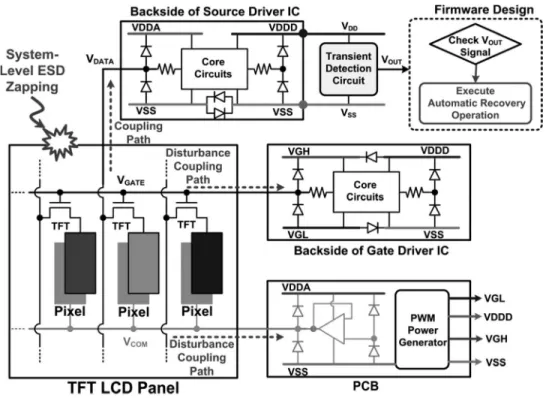
Fig. 3. Hardware/firmware system codesign with transient detection circuit in display panel product.
In this paper, a new on-chip 4-bit transient-to-digital con-verter composed of capacitor-resistor (CR)-based transient detection circuits is proposed to detect the fast electrical transients and provide output digital codes under system-level ESD stresses. The new proposed converter is designed to reduce the large decoupling capacitor used in a noise filter network. Experimental results in a 0.13-µm CMOS process with 1.8-V devices have verified that the output digital codes can correctly correspond with the magnitude of fast electrical transients under system-level ESD tests.
II. DISPLAYPANELPROTECTIONDESIGN
AGAINSTSYSTEM-LEVELESD STRESS
It had been proven that the hardware/firmware codesign can effectively improve the robustness of the industrial products against electrical transient disturbance. For a display system protection design with a thin-film transistor liquid crystal dis-play panel, multiple power systems are needed for electri-cal display functions, as shown in Fig. 3. For example, in the backside of a source driver IC, the analog power line (VDDA) is used for digital-to-analog converter circuit, and the digital power line (VDDD) is used for shifter register to store display signals. A transient detection circuit, designed for detecting and memorizing the occurrence of ESD-induced transient disturbance, can connect with a 1.8-V VDDD power line to implement the hardware/firmware protection design in a display system. The detection results from the detection circuit can be temporarily stored as a system recovery index for firmware check, as shown in Fig. 3. In the beginning, the output(VOUT) state of the detection circuit is initially reset to logic “1.” When the electrical transients happen, the detection circuit can detect the occurrence of system-level ESD-induced
Fig. 4. New proposed on-chip CR-based transient detection circuit.
transient disturbance and transit the output state (VOUT) to logic “0.” At this moment, the firmware index is also changed to logic “0” to initiate automatic recovery operation to restore the microelectronic display system to a desired stable state as soon as possible. After the automatic recovery operation, the output of the detection circuit and the system recovery index are reset to logic “1” again for detecting the next ESD-induced electrical transient disturbance events.
III. NEWON-CHIPCR-BASEDTRANSIENT
DETECTIONCIRCUIT A. Circuit Implementation
Fig. 4 shows the new proposed on-chip CR-based ESD detection circuit. The CR-based circuit structure is designed to realize the transient detection function. The NMOS (Mnr) is used to provide the initial reset function to set the initial volt-ages at nodeVOUTand nodeVAas 1.8 V with theVDDof 1.8 V
in a 0.13-µm CMOS process. In Fig. 4, node VG is biased at
VSS during the normal operating condition. Under the system-level ESD stress with an overshooting ESD voltage, nodeVG
1280 IEEE TRANSACTIONS ON INDUSTRIAL ELECTRONICS, VOL. 59, NO. 2, FEBRUARY 2012
will be coupled with a positive voltage. Then, the NMOS device (Mn1) can be turned on by the overshooting ESD voltage to pull down the voltage level at nodeVA. Therefore, the logic level
stored at nodeVAcan be changed from logic “1” to logic “0”
to memorize the ESD-induced transient disturbance. With the buffer inverters, the output voltage is finally changed from 1.8 to 0 V to detect the occurrence of system-level ESD events. Furthermore, by different combination design ofR1 and R2, the ESD energy coupled to nodeVGcan be adjusted. Therefore,
the minimum ESD voltage to cause transition at the output (VOUT) of the proposed detection circuit can be designed by this resistive voltage divider technique.
B. HSPICE Simulation
It has been investigated that the underdamped sinusoidal voltage waveform has been observed on the power line of CMOS IC during the system-level ESD stress. Therefore, a sinusoidal time-dependent voltage source given by
V (t)=V0+ Va· sin (2πf(t − td)) · exp (−(t − td)Da) (1)
is used to simulate the ESD-induced transient disturbance coupled on the power lines of the proposed detection circuit. With the proper parameters (including the applied voltage amplitude Va, initial dc voltage V0, damping factor Da =
2 × 10⁷ s−1, frequency f = 50 MHz, and time delay t d=
300 ns), the underdamped sinusoidal voltage can be used to simulate the electrical transient waveforms under system-level ESD tests.
The simulatedVDD andVOUT waveforms of the proposed detection circuit with a positive-going (negative-going) under-damped sinusoidal voltage onVDDline are shown in Fig. 5(a) and (b). The positive-going underdamped sinusoidal voltage with an amplitude of +3 V (−3 V) is used to simulate the coupling ESD transient noise under the system-level ESD test. From the simulated waveforms, VDD begins to increase (decrease) rapidly from 1.8 V.VOUTalso acts with a positive-going (negative-positive-going) underdamped sinusoidal voltage wave-form during the simulated system-level ESD events on VDD line. After this disturbance duration, VDD returns to its nor-mal voltage level of 1.8 V, and the output state (VOUT) of the detection circuit is changed from 1.8 to 0 V, as shown in Fig. 5(a) and (b). As a result, the detection circuit can detect the occurrence of simulated ESD-induced electrical tran-sients. Furthermore, with increasing resistor ratio of R1/R2, the ESD energy coupled to nodeVG will be decreased, and the minimum ESD amplitude(≡ Va(min)) to cause transition of the proposed detection circuit will be increased, as shown in Fig. 6.
IV. EXPERIMENTALRESULTS
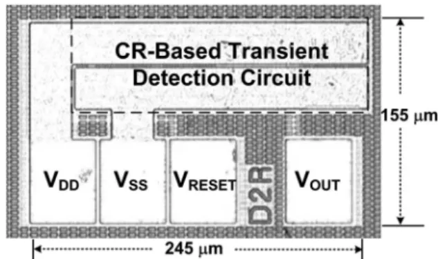
The proposed detection circuit has been designed and fab-ricated in a 0.13-µm CMOS process. The fabricated chip for transient disturbance tests is shown in Fig. 7. The silicon area of the proposed on-chip detection circuit is245 µm × 155 µm.
Fig. 5. Simulated VDD and VOUT waveforms of the new proposed on-chip CR-based transient detection circuit under system-level ESD test with (a) positive-going and (b) negative-going underdamped sinusoidal voltages.
Fig. 6. Relation between resistor ratio and minimum simulated amplitude.
Fig. 7. Chip photo of the new proposed on-chip CR-based transient detection circuits fabricated in a 0.13-µm CMOS process.
Fig. 8. Measurement setup for TLU test on display panel. A. TLU Test
Fig. 8 shows such a component-level transient-induced latchup (TLU) measurement setup on a display system. An ESD simulator (ETS910A) is used to generate the TLU-triggering source,VCharge, to produce an underdamped sinusoidal volt-age stimulus. Through applying a positive (negative) charged voltageVCharge, the intended positive-going (negative-going) underdamped sinusoidal voltage can be generated similar to transient disturbance generated from the ESD gun. In the equivalent circuit of a machine-mode module shown in the inset of Fig. 8, a charging capacitance of 200 pF is used to store charges for the TLU-triggering source,VCharge, and then, these stored charges are discharged to a 1.8-V power line of the display system through the relay. The intended underdamped sinusoidal voltage can be produced to simulate the transient voltage on the power pins of CMOS ICs under the system-level ESD test.
Fig. 9(a) and (b) shows the measuredVDD andVOUT tran-sient responses of the proposed detection circuit under the TLU test withVChargeof+200 and −200 V, respectively. As shown in Fig. 9(a), under the TLU test withVChargeof+200 V, VDD begins to increase rapidly from 1.8 V with a positive-going underdamped sinusoidal voltage waveform. During the TLU test,VOUTis influenced simultaneously with a positive-going underdamped sinusoidal voltage coupled to VDD power line. After the TLU test with the VCharge of +200 V, the output voltage (VOUT) of the proposed detection circuit can transit from 1.8 to 0 V. In Fig. 9(b), under the TLU test withVCharge of −200 V, VDD begins to decrease rapidly from 1.8 V with a negative-going underdamped sinusoidal voltage waveform. During the TLU test,VOUTis influenced simultaneously with a negative-going underdamped sinusoidal voltage coupled to VDDpower line. After the TLU test with theVChargeof−200 V, the output voltage(VOUT) of the proposed detection circuit can transit from 1.8 to 0 V.
From the TLU test results, the proposed detection circuit can successfully memorize the occurrence of electrical transients. With positive or negative underdamped sinusoidal voltages coupled toVDDpower line, the output voltages(VOUT) of the proposed detection circuit can both change from logic“1” to logic“0” after TLU tests.
Fig. 9. MeasuredVDDandVOUTwaveforms on the new proposed CR-based transient detection circuit under TLU tests with VCharge of (a) +200 and (b)−200 V.
B. System-Level ESD Test
In IEC 61000-4-2, two test modes have been specified, which are the air-discharge test mode and the contact-discharge test mode [7]. In the case of air-discharge test mode, the round discharge tip should be approached as fast as possible to touch the EUT. The air discharge is actuated by a spark to the EUT, and the ESD energy holding time is at least 5 s. In the case of contact-discharge test mode, the sharp discharge tip is used to simulate the mechanical ESD damage on the EUT. The contact discharge is applied to the conductive surfaces of the EUT (direct application) or to the horizontal or vertical coupling planes (indirect application). The measurement setup of the system-level ESD test consists of a wooden table on the grounded reference plane (GRP). In addition, an insulating plane of 0.5-mm thickness is used to separate the EUT/cables from the HCP. The HCP is connected to the GRP with two 470-kΩ resistors in series.
Fig. 10 shows the measurement setup of the system-level ESD test standard with an air-discharge test mode in a dis-play system. When the ESD gun is approaching the EUT, the electromagnetic interference coming from the ESD gun will be coupled into all CMOS ICs inside EUT. The power lines of CMOS ICs inside EUT will be disturbed by the ESD-coupled energy.
With such a measurement setup shown in Fig. 10, the cir-cuit function of the proposed detection circir-cuit after system-level ESD tests can be evaluated. Before each system-system-level ESD test, the initial output voltage (VOUT) of the proposed
1282 IEEE TRANSACTIONS ON INDUSTRIAL ELECTRONICS, VOL. 59, NO. 2, FEBRUARY 2012
Fig. 10. Measurement setup for system-level ESD test with air-discharge test mode [7] to evaluate the detection function of the fabricated on-chip transient detection circuit on display system application.
detection circuit is reset to 1.8 V. After each system-level ESD test, the output voltage (VOUT) level is monitored to check the final voltage level and to verify the detection function.
The measuredVDD and VOUT waveforms of the proposed detection circuit under a system-level ESD test with an ESD voltage of +4 kV are shown in Fig. 11(a). VDD begins to increase rapidly from the normal voltage of+1.8 V. Meanwhile, VOUTis disturbed under such a high-energy ESD stress. During the period with positive-going ESD-induced electrical transient disturbance, VDD and VOUT are influenced simultaneously. Finally, the output voltage(VOUT) of the proposed detection circuit transits from 1.8 to 0 V. Therefore, the proposed detec-tion circuit can sense the positive-going electrical transient on the power line and memorize the occurrence of the system-level ESD event.
The measuredVDDandVOUTtransient voltage waveforms of the proposed detection circuit with the ESD voltage of−4 kV under a system-level ESD test are shown in Fig. 11(b). Dur-ing the negative-goDur-ing ESD-induced electrical transient distur-bance onVDDpower line, VOUTis disturbed simultaneously. After the system-level ESD test with the ESD voltage of−4 kV, VDD returns to the operation voltage level of 1.8 V, andVOUT transits from logic“1” to logic“0.” The detection function of the proposed on-chip detection circuit after the system-level ESD tests has been verified by both the experimental results in silicon chip and HSPICE simulation.
For advanced system-level ESD verification on industrial display products, there are nine zapping locations defined on the display panels with air-discharge test mode, as shown in Fig. 12.
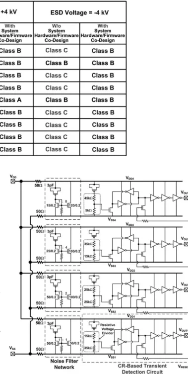
In the IEC 61000-4-2 standard, for microelectronic products after system-level ESD zapping, class A, class B, and class C denote normal performance, automatic recovery, and manual recovery, respectively. By using the output digital codes as the firmware index, the display panel can automatically recover all electrical functions to successfully release the locked or frozen states caused by system-level ESD transient
distur-Fig. 11. MeasuredVDDandVOUTtransient voltage waveforms of the new proposed detection circuit under system-level ESD tests with ESD voltages of (a)+4 and (b) −4 kV.
Fig. 12. Test point definition on display panel under system-level ESD tests with air-discharge test mode.
bance. Table I shows the comparison among the measured results between the display panel without and with system hardware/firmware codesign via the proposed detection circuit. The display system criterion can be improved from “class C” to “class B” to meet the typical specifications of commercial microelectronic products.
V. TRANSIENT-TO-DIGITALCONVERTER A. Circuit Implementation
It has been investigated that noise filter networks can reduce the susceptibility of CMOS ICs against electrical transients by
TABLE I
MEASUREDRESULTS OFDISPLAYPANELWITHOUT ANDWITHSYSTEMHARDWARE/FIRMWARECODESIGN
Fig. 13. Relation between current-gain device width ratio and the simulated peak-to-peak voltage value of degraded transient disturbance.
decoupling or bypassing noise energy. In the previous design, a 10-pF on-chip decoupling capacitor is used in a noise filter network [30]. In this paper, a 3-pF on-chip capacitor(C1) with a current mirror is adopted to replace the large decoupling capacitor between power lines, as shown in the inset of Fig. 13. If the current-gain device width ratio isN, the capacitor (C1) can be scaled up by a factor ofN + 1. As shown in Fig. 13, when the underdamped sinusoidal voltage with an amplitude of +10 V is applied on VDDpower line, the transient disturbance coupled on internal power line(VDD(i)) will be decreased by increasing the current-gain device width ratio of the current mirror.
Fig. 14 shows the proposed on-chip 4-bit transient-to-digital converter consisted of four CR-based transient detection cir-cuits and four different noise filter networks. With different device ratios in the current mirror, different ESD levels on VDD and VSS will reach to each transient detection circuit. For the CR-based circuit structure shown in Fig. 4, the ESD energy coupled to nodeVGcan be further adjusted by different resistive voltage dividers. Therefore, the minimum ESD voltage
Fig. 14. Proposed 4-bit transient-to-digital converter realized with four CR-based transient detection circuits and four different noise filter networks.
to cause transition at the output(VOUT) of the detection circuit can be designed for each stage in the transient-to-digital con-verter. Under the system-level ESD zapping conditions, the four transient detection circuits will have different output voltage responses.
Therefore, by combining different noise filter networks, the proposed on-chip transient-to-digital converter can be designed to detect different ESD voltage levels and transfer output volt-ages into digital codes under system-level ESD tests.
1284 IEEE TRANSACTIONS ON INDUSTRIAL ELECTRONICS, VOL. 59, NO. 2, FEBRUARY 2012
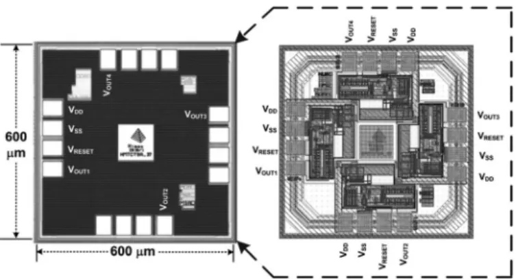
Fig. 15. Chip photo and layout of the proposed 4-bit transient-to-digital converter realized in a 0.13-µm CMOS process.
B. Experimental Results
The layout of the proposed on-chip 4-bit transient-to-digital converter is consisted of four unit cells of the CR-based detection circuit and different noise filter networks. The silicon area is600 µm × 600 µm, as shown in Fig. 15. The system-level ESD test standard with indirect contact-discharge test mode is used to verify the output digital codes.
The measured VOUT1, VOUT2, VOUT3, and VOUT4 wave-forms of the proposed 4-bit transient-to-digital converter under a system-level ESD test with an ESD voltage of +0.7 kV zapping on the HCP are shown in Fig. 16(a). During the fast transient of ESD stress,VOUT1, VOUT2,VOUT3, and VOUT4 are disturbed simultaneously during VDD/VSS electrical dis-turbance. Finally, when VDD returns to the normal operation voltage level of 1.8 V, VOUT1 will be changed from 1.8 to 0 V, andVOUT2, VOUT3, and VOUT4 are still kept at 1.8 V. Therefore, the detection output voltages can transfer the +0.7-kV ESD voltage level into a digital code of “1110.”
Similarly, under a system-level ESD test with ESD voltages of +0.8, +1.0, and +1.3 kV, the transferred digital codes generated by the proposed 4-bit transient-to-digital converter are “1100,” “1000,” and “0000,” as shown in Fig. 16(b)–(d), respectively. Therefore, the proposed on-chip converter can successfully transfer different positive ESD voltage levels into different digital codes. The digital code goes from “1110” to “0000” as the magnitude of positive ESD voltage increases from+0.7 to +1.3 kV.
The measuredVOUT1,VOUT2,VOUT3, andVOUT4 voltage waveforms of the proposed transient-to-digital converter under a system-level ESD test with an ESD voltage of−0.2 kV are shown in Fig. 17(a). During the fast transient of ESD stress, all transient detection circuits are affected by ESD-induced transient disturbance coupled on VDD line. Finally, VOUT1 transits from logic “1” to logic “0,” while VOUT2, VOUT3, andVOUT4 are still kept at logic “1” states. Therefore, under the system-level ESD test with the ESD voltage of−0.2 kV, the output responses of the proposed 4-bit converter can be transferred into a digital code of “1110.”
Similarly, under a system-level ESD test with ESD voltages of−0.3, −0.6, and −1.1 kV, the transferred digital codes gener-ated by proposed 4-bit transient-to-digital converter are “1100,” “1000,” and “0000,” as shown in Fig. 17(b)–(d), respectively.
Fig. 16. MeasuredVOUT1,VOUT2,VOUT3, andVOUT4transient voltage waveforms under system-level ESD test with ESD voltages of (a) +0.7, (a)+0.8, (a) +1.0, and (d) +1.3 kV zapping on the HCP.
Fig. 17. MeasuredVOUT1,VOUT2,VOUT3, andVOUT4transient voltage waveforms under system-level ESD test with ESD voltages of (a) −0.2, (a)−0.3, (a) −0.6, and (d) −1.1 kV zapping on the HCP.
TABLE II
ESD-VOLTAGE-TO-DIGITAL-CODECHARACTERISTIC
From the measurement results, the detection and response time of the proposed converter is about 300 ns.
Table II shows the ESD-voltage-to-digital-code character-istic of the proposed 4-bit transient-to-digital converter. The digital code goes from “1110” to “0000” as the magnitude of ESD voltage increases from+0.7 to +1.3 kV and from −0.2 to −1.1 kV. Different ESD voltage levels can successfully respond to different digital codes.
C. Hardware/Firmware Codesign
To perform the hardware/firmware codesign, the digital codes from the transient-to-digital converter can be temporarily stored as a system recovery index for firmware check. The display system can be programmed to execute different recov-ery procedures according to different digital codes with the consideration of system recovery time and energy saving.
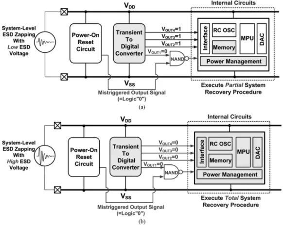
In the beginning, the output digital code is set as “1111.” When the electrical transients happen, the transient-to-digital converter can detect the occurrence of system-level electrical transient disturbance and transfer the ESD voltage levels into digital codes. At this moment, the firmware index is also changed to initiate a system recovery procedure to restore the system to a known stable state as soon as possible. According to the different digital codes, the firmware can program the corresponding system recovery procedures. For example, under a system-level ESD test with low ESD voltage zapping, the transferred digital code is “1110,” and the firmware can execute a partial system recovery procedure in a display panel, as shown in Fig. 18(a). With high ESD zapping, the transferred digital code is “0000,” and the firmware can execute a total system recovery procedure, as shown in Fig. 18(b).
For system initial state setting, a power-on reset circuit can further be designed into a hardware/firmware codesign to set the initial digital code into “1111.” However, there are some mistriggered conditions for the power-on reset circuit. For ex-ample, a sudden surge can result in a very short interval between the power-down and power-up transitions. Such short interval of power-off creates difficult situations for some power-on reset circuits to work properly. Therefore, theNANDlogic gate circuit can be further added into the hardware/firmware codesign flow. TheVOUT1 signal of the transient-to-digital converter and the output signal of the power-on reset circuit are connected as the input signals of theNANDlogic gate. When electrical transient disturbance happens, the system recovery procedure can be still initiated to protect microelectronic display products against the electrical transitions caused by system-level ESD events.
1286 IEEE TRANSACTIONS ON INDUSTRIAL ELECTRONICS, VOL. 59, NO. 2, FEBRUARY 2012
Fig. 18. Hardware/firmware operation in display panel system during (a) low and (b) high system-level ESD zapping conditions.
VI. DISCUSSION
In this paper, the proposed transient-to-digital converter can successfully transfer different ESD voltage levels into different digital codes. The modified converter to distinguish positive and negative ESD voltages with symmetric digital codes will be further studied in our future works. Furthermore, with the on-chip ESD power clamp circuit and the CR-based transient detection circuit in a chip together, it can be further considered to share the sameRC triggering circuit to provide on-chip ESD protection and transient disturbance detection.
VII. CONCLUSION
An on-chip transient-to-digital converter composed of four CR-based transient detection circuits and four different noise filter networks has been successfully verified in this paper. The measured results show that the output digital codes can correspond to the different magnitudes of the ESD voltages under system-level ESD tests. These output digital codes can be used as the firmware index to execute different autorecovery procedures of industrial products. The proposed circuit has been practically applied to the display panels of mobile phones to release the system locked or frozen states caused by ESD-induced transient disturbance under system-level ESD tests.
ACKNOWLEDGMENT
The authors would like to thank C.-C. Tsai and Dr. T.-Y. Chen for their valuable technical discussions.
REFERENCES
[1] A. Ristow, M. Begovic, A. Pregelj, and A. Rohatgi, “Development of a methodology for improving photovoltaic inverter reliability,” IEEE Trans. Ind. Electron., vol. 55, no. 7, pp. 2581–2592, Jul. 2008.
[2] C. Rodriguez and G. Amaratunga, “Long-lifetime power inverter for photovoltaic ac modules,” IEEE Trans. Ind. Electron., vol. 55, no. 7, pp. 2593–2601, Jul. 2008.
[3] H. Hansson, T. Nolte, C. Norstrom, and S. Punnekkat, “Integrating re-liability and timing analysis of CAN-based systems,” IEEE Trans. Ind. Electron., vol. 49, no. 6, pp. 1240–1250, Dec. 2002.
[4] P. Hammond, “Enhancing the reliability of modular medium-voltage drives,” IEEE Trans. Ind. Electron., vol. 49, no. 5, pp. 948–954, Oct. 2002. [5] S. Petrovic, A. Ramirez, T. Maudie, D. Stanerson, J. Wertz, G. Bitko, J. Matkin, and D. Monk, “Reliability test methods for media-compatible pressure sensors,” IEEE Trans. Ind. Electron., vol. 45, no. 6, pp. 877–885, Dec. 1998.
[6] M.-D. Ker and S.-F. Hsu, Transient-Induced Latchup in CMOS Integrated Circuits. Hoboken, NJ: Wiley, 2009.
[7] EMC—Part 4-2: Testing and Measurement Techniques—Electrostatic Discharge Immunity Test, Int. Std. IEC 61 000-4-2, 2008.
[8] G. Escobar, A. Valdez, J. Leyva-Ramos, and P. Mattavelli, “Repetitive-based controller for a UPS inverter to compensate unbalance and har-monic distortion,” IEEE Trans. Ind. Electron., vol. 54, no. 1, pp. 504–510, Feb. 2007.
[9] E. Monmasson and M. Cirstea, “FPGA design methodology for industrial control systems—A review,” IEEE Trans. Ind. Electron., vol. 54, no. 4, pp. 1824–1842, Aug. 2007.
[10] J. Rodriguez, J. Dixon, J. Espinoza, J. Pontt, and P. Lezana, “PWM re-generative rectifiers: State of the art,” IEEE Trans. Ind. Electron., vol. 52, no. 1, pp. 5–22, Feb. 2005.
[11] G. Buja and M. Kazmierkowski, “Direct torque control of PWM inverter-fed AC motors—A survey,” IEEE Trans. Ind. Electron., vol. 51, no. 4, pp. 744–757, Aug. 2004.
[12] R. Daily and D. Bevly, “The use of GPS for vehicle stability control sys– tems,” IEEE Trans. Ind. Electron., vol. 51, no. 2, pp. 270–277, Apr. 2004. [13] S. Voldman, ESD: Circuits and Devices. Hoboken, NJ: Wiley, 2006. [14] K. Muhonen, P. Erie, N. Peachey, and A. Testin, “Human metal model
(HMM) testing, challenges to using ESD guns,” in Proc. EOS/ESD Symp., 2009, pp. 387–395.
[15] D. Liu, D. Pommerenke, S. Kwon, and K. Martwick, “Full wave model for simulating a Noiseken ESD generator parameters,” in Proc. IEEE Int. Symp. EMC, 2009, pp. 334–339.
[16] G. Muchaidze, J. Koo, Q. Cai, T. Li, L. Han, A. Martwick, K. Wang, J. Min, J. Drewniak, and D. Pommerenke, “Susceptibility scanning as a failure analysis tool for system-level electrostatic discharge (ESD) prob-lems,” IEEE Trans. Electromagn. Compat., vol. 50, no. 2, pp. 268–276, May 2008.
[17] N. Lacrampe, F. Caignet, M. Bafleur, N. Nolhier, and N. Mauran, “Characterization and modeling methodology for IC’s ESD susceptibility at system level using VF-TLP tester,” in Proc. EOS/ESD Symp., 2007, pp. 304–310.
[18] M. Honda, “EMI power measurements of ESD radiated fields,” in Proc. EOS/ESD Symp., 2006, pp. 160–165.
[19] M.-D. Ker and S.-F. Hsu, “Component-level measurement for transient– induced latch–up in CMOS ICs under system-level ESD considerations,” IEEE Trans. Device Mater. Rel., vol. 6, no. 3, pp. 461–472, Sep. 2006. [20] T.-H. Wang, W.-H. Ho, and L.-C. Chen, “On-chip system ESD
pro-tection design for STN LCD drivers,” in Proc. EOS/ESD Symp., 2005, pp. 316–322.
[21] M.-D. Ker and S.-F. Hsu, “Physical mechanism and device simulation on transient-induced latchup in CMOS ICs under system-level ESD test,” IEEE Trans. Electron Devices, vol. 52, no. 8, pp. 1821–1831, Aug. 2005. [22] W. Stadler, S. Bargstadt-Franke, T. Brodbeck, R. Gaertner, M. Goroll, H. Gosner, N. Jensen, and C. Muller, “From the ESD robustness of products to the system-level ESD robustness,” in Proc. EOS/ESD Symp., 2004, pp. 67–74.
[23] N. Shimoyama, M. Tanno, S. Shigematsu, H. Morimura, Y. Okazaki, and K. Machida, “Evaluation of ESD hardness for fingerprint sensor LSIs,” in Proc. EOS/ESD Symp., 2004, pp. 75–81.
[24] M.-D. Ker, “Whole-chip ESD protection design with efficient VDD-to-VSS clamp circuit for submicron CMOS VLSI,” IEEE Trans. Electron Devices, vol. 46, no. 1, pp. 173–183, Jan. 1999.
[25] M.-D. Ker and S.-F. Hsu, “Evaluation on board-level noise filter networks to suppress transient-induced latchup in CMOS ICs under system-level ESD test,” IEEE Trans. Electromagn. Compat., vol. 48, no. 1, pp. 161– 171, Feb. 2006.
[26] H. Ott, Noise Reduction Techniques in Electronic Systems, 2nd ed. Hoboken, NJ: Wiley, 1988.
[27] M. Montrose, Printed Circuit Board Design Techniques for EMC Compli-ance. Piscataway, NJ: IEEE Press, 2000.
[28] M.-D. Ker and C.-C. Yen, “New transient detection circuit for on-chip protection design against system-level electrical transient disturbance,” IEEE Trans. Ind. Electron., vol. 57, no. 10, pp. 3533–3543, Oct. 2010. [29] M.-D. Ker, W.-Y. Lin, C.-C. Yen, C.-M. Yang, T.-Y. Chen, and S.-F. Chen,
“On-chip ESD detection circuit for system-level ESD protection design,” in Proc. IEEE ICSICT, 2010, pp. 1584–1587.
[30] M.-D. Ker and C.-C. Yen, “Transient-to-digital converter for system-level ESD protection in CMOS integrated circuits,” IEEE Trans. Electromagn. Compat., vol. 51, no. 3, pp. 620–630, Aug. 2009.
[31] M.-D. Ker, C.-C. Yen, and P.-C. Shin, “On-chip transient detection circuit for system-level ESD protection to meet electromagnetic compatibility regulation,” IEEE Trans. Electromagn. Compat., vol. 50, no. 1, pp. 13– 21, Feb. 2008.
Ming-Dou Ker (S’92–M’94–SM’97–F’08) received
the Ph.D. degree from the Institute of Electronics, National Chiao-Tung University, Hsinchu, Taiwan, in 1993.
He was the Department Manager of the VLSI Design Division, Computer and Communication Re-search Laboratories, Industrial Technology ReRe-search Institute, Hsinchu. Since 2004, he has been a Full Professor with the Department of Electronics Engi-neering, National Chiao-Tung University. In 2008, he was rotated to be a Chair Professor with and Vice President of I-Shou University, Kaohsiung, Taiwan. Currently, he is a Distinguished Professor with the Department of Electronics Engineering, National Chiao-Tung University, and serves as the Executive Director of the National Science and Technology Program on Nanotechnology, Taiwan. In the technical field of reliability and quality design for microelectronic circuits and systems, he has published over 400 technical papers in international journals and conferences. He has proposed many solutions to improve the reliability and quality of integrated circuits, which have been granted with 185 U.S. patents and 157 Taiwan patents. He had been invited to teach and/or to consult the reliability and quality design for integrated circuits by hundreds of design houses and semiconductor companies in the worldwide IC industry. His current research interests include reliability and quality design for nanoelectronics and gigascale systems, high-speed and mixed-voltage I/O interface circuits, on-glass circuits for system-on-panel applications, and biomimetic circuits and systems for intelligent prosthesis.
Dr. Ker has served as a member of the Technical Program Committee and the Session Chair of numerous international conferences for many years. He served as an Associate Editor for the IEEE TRANSACTIONS ON VLSI SYSTEMS
from 2006 to 2007. He was selected as the Distinguished Lecturer in the IEEE Circuits and Systems Society (2006–2007) and in the IEEE Electron Devices Society (2008-2011). He was the President of Foundation in Taiwan ESD Association. In 2009, he was awarded as one of the top ten Distinguished Inventors in Taiwan.
Cheng-Cheng Yen (S’07–M’09) received the B.S.
degree from the Department of Electrical and Control Engineering, National Chiao-Tung Univer-sity, Hsinchu, Taiwan, in 1998 and the M.S. and Ph.D. degrees from the Institute of Electronics, Na-tional Chiao-Tung University, in 2000 and 2009, respectively.
He is currently a Postdoctoral Researcher with the National Chiao-Tung University. His current re-search interests include transient detection circuits and IC reliability.
![Fig. 1 shows the measurement setup of the system-level ESD test with the indirect contact-discharge test mode [7]](https://thumb-ap.123doks.com/thumbv2/9libinfo/7688394.142928/1.891.462.836.256.456/fig-shows-measurement-setup-level-indirect-contact-discharge.webp)