218 IEEE ELECTRON DEVICE LETTERS, VOL. 21, NO. 5, MAY 2000
Retardation in the Chemical–Mechanical Polish of
the Boron-Doped Polysilicon and Silicon
Wen Luh Yang, Chih-Yuan Cheng, Ming-Shih Tsai, Don-Gey Liu, and Ming-Sun Shieh
Abstract—This letter reports on the chemical–mechanical
pol-ishing (CMP) of boron-doped polysilicon and silicon. Successive polishing was carried out to investigate how the removal rate cor-relates to the boron concentration as a function of depth in the polysilicon and crystalline silicon. It is found that the removal of boron-doped samples is significantly retarded and strongly corre-lated with the doping concentration. To the author’s knowledge, this work is the first report discussing the retardation effect of boron in the Si-CMP process. This effect is attributed to the acti-vated dopant atoms which are conjectured to inhibit the hydrolysis reaction of Si–Si bonding in the alkaline aqueous solution. In our study, the retardation effect is evident for the boron concentration higher than5 1018cm 3. As a consequence, it may become an issue in CMP process for those layers of selected or complemented doping.
Index Terms—Boron, chemical–mechanical polish,
planariza-tion process, semiconductor impurities, semiconductor process modeling.
I. INTRODUCTION
C
HEMICAL–MECHANICAL POLISH (CMP) is a useful tool for global surface planarization in the semiconductor industry [1]. The main applications of CMP are planarization of interlayer dielectric (ILD) and interconnection metal layers in the multilevel technology. Trench isolation can also be improved by CMP [2]. Recently, CMP technique has been considered to improve the surface roughness of the poly-Si film to increase its carrier mobility [3]. The dielectric films whether deposited or thermally grown on such polished poly-Si present excellent breakdown properties and much lower leakage [4], [5]. How-ever, the details of Si-CMP process, especially for the dopants involved in the reaction, are seldom discussed and less under-stood.In this letter, the polishing characteristics of the boron-doped poly-Si and crystalline silicon in the CMP process are studied. Successive CMP were performed for each sample to investigate the profile of removal rates along the layer depth. Effects of boron implanted in the samples were studied by comparing the
Manuscript received October 15, 1999; revised January 20, 2000. This work was supported by the National Nano-Device Laboratory under Contract NDL-88-C-046 and supported in part by Feng Chia University and the National Science Council, R.O.C. The review of this letter was arranged by Editor H.-H. Vuong.
W. L. Yang, C.-Y Cheng, and D.-G. Liu are with the Institute and Depart-ment of Electrical Engineering, Feng Chia University, 40724 Taichung, Taiwan, R.O.C. (e-mail: [email protected])
M.-S. Tsai is with the National Nano-Device Laboratory, 300 Hsinchu, Taiwan, R.O.C.
M.-S. Shieh is with the National Chiaotung University, 300 Hsinchu, Taiwan, R.O.C.
Publisher Item Identifier S 0741-3106(00)03893-3.
doped and undoped samples. It is found that the removal rates for the boron-doped samples are significantly lower as com-pared with the undoped samples. The influence of boron con-centration will be quantitatively analyzed by comparing the sec-ondary-ion mass spectroscopy (SIMS) profiles and the resulting removal rates. It is found that the removal rates strongly corre-late with the boron concentration. Similar phenomena were also found in our study in the wet etching of p-type Si in the alkaline aqueous solutions. In this paper, the effects of boron on the re-moval of Si will be demonstrated. The possible role of boron in the CMP process will also be discussed.
II. SAMPLEPREPERATION
In this study, both poly-Si films and Si substrates are under investigation. For preparation of p-type poly-Si, a 100 nm wet oxide layer was first grown on the n-type (100) Si wafers to isolate the effects from the substrate. After that, a 600-nm poly-Si film was deposited on the oxidized substrate in an LPCVD system at 620 C. Samples were then implanted with cm boron or arsenic of 50 and 100 keV, respectively, for the following polishing experiments. The doped impurities were activated by two steps, i.e., furnace annealing at 700 C for 1 h and then rapid thermal annealing at 950 C for 25 s. In order to show the effect of dopant impurities, a control sample with a layer of undoped poly-Si was also fabricated. Except for the ion implantation, such control sample undergoes all the same processes as the other doped samples.
For all samples, the poly-Si layer was trenched to form equally spaced parallel stripes on the oxide layer by pho-tolithography and ECR plasma etching. These stripes are 20- m wide and spaced by 20 m. The step heights of the patterned poly-Si were measured by a surface profilermeter. Since the oxide layer can be a stop layer in the later CMP process, the obtained step heights are just the thickness of the poly-Si. For each polishing, changes of step heights were averaged to estimate the removal rate for that run. Successive removal rates were obtained for each sample to investigate the depth-dependent relation along the substrate side.
All the CMP experiments were carried out on an IPEC/Westech 372M polisher. The polishing parameters were kept fixed for all CMP processes. These parameters such as down pressure, platen and carrier rotation speed, slurry flow rates and polishing time were set to be 3 psi, 50 rpm, 60 rpm, 150 ml/min, and 30 s, respectively. Rodel Politex Reg. E polish pad and Rodel R200-T3 carrier film were used in our polish process. In this study, CABOT SC1 slurry, which contains 30 wt.% fumed silica abrasives suspended in the
YANG et al.: BORON-DOPED POLYSILICON AND SILICON 219
Fig. 1. Removal rates for boron-, arsenic-doped and undoped poly-Si layers. The inset is the removal rates for phosphorus- and boron-doped silicon wafers.
KOH aqueous solution, was diluted with DI water in 1 : 10 volume ratio to make its pH value around 10–11. After each polishing, the samples were cleaned for thereafter step height measurements by the diluted NH OH of a concentration less than 3%. Since all the parameters in our experiment were the same for each sample and each run, interference caused from the equipment variations or transients can be kept as low as possible. Therefore, discrepancies between the removal rates of the samples can be mainly attributed to the dopant impurities.
Distributions of boron were analyzed by SIMS. They are used to investigate the relation between the boron concentration and the removal rates.
The same conditions as described above were also used in the study of the single crystalline Si wafers. However, only p-type and n-type (100) substrates were verified. These substrates are doped by boron and phosphorus with resistivities around 20 and 6 -cm, respectively.
III. RESULTS ANDDISCUSSION
Fig. 1 shows the comparison of removal of doped and un-doped poly-Si films. Each removal rate is drawn with its cor-responding depth. Such depth is estimated as the total removed thickness in previous runs plus the half of the currently removed layer. As seen in Fig. 1, the removal rates for undoped and ar-senic-doped samples are reduced down from the surface and kept almost constant around 1200 Å/min. We have observed the surface topography of a sample by the atomic force micro-scope (AFM) and confirm that the rougher surface will result in a higher removal rate. Therefore, such reduction of removal rate can be mainly attributed to the progressive improvement of surface roughness. It is also noted that the initial removal rates for each sample are nearly the same around 2000 Å/min. This fact reveals that the initial surfaces of doped or undoped samples are very similar. However, seeing the curves in Fig. 1, the trend of the boron-doped poly-Si is much different from the other two and can not be interpreted simply by the effect of surface rough-ness. The removal rate is significantly reduced near the depth of 0.2 m where the peak concentration of boron is expected. This finding indicates that, in addition to the surface roughness, the
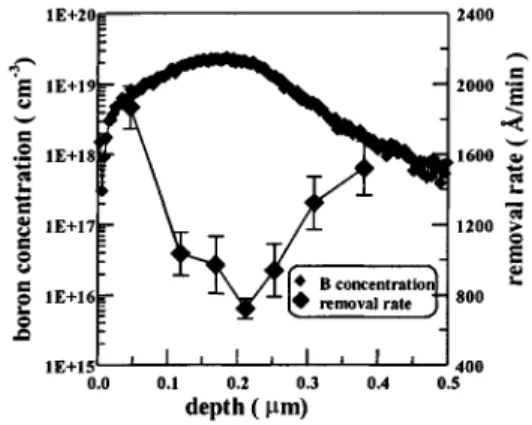
Fig. 2. Comparison of the removal rates and boron concentration.
polishing is strongly affected by the boron. The inset in Fig. 1 shows a similar result for the (100) n- and p-type Si wafers. The same trend can be concluded as that the p-type substrate exhibits lower removal rates.
The effect of boron to retard the removal of Si will be more obvious in Fig. 2. Fig. 2 demonstrates the correlation between the removal rates and the SIMS profile of boron. The removal rate is reduced as the boron concentration increases. Let us take the difference between the curves for the boron-doped and un-doped samples in Fig. 1; the effect of surface roughness can then be eliminated and the effect of the boron on the removal of Si will be manifest. By comparing the above result and the SIMS profile in Fig. 2, retardation is found to be more pronounced for boron concentration higher than cm .
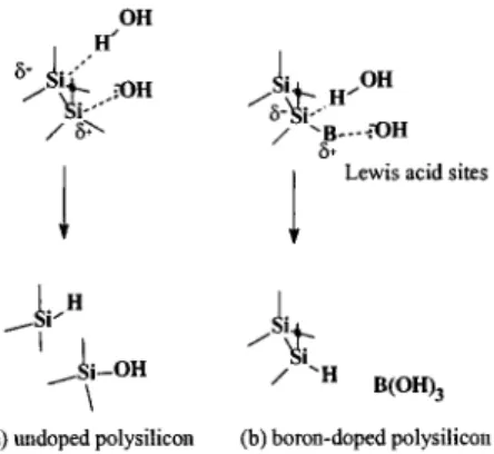
All the above results point out that the retardation of silicon polishing is due to the presence of boron and is less depen-dent on the arsenic concentration. The above finding also tell us that even the amount of impurity are relatively insignificant in the Si, the chemical characteristics of Si will be modified seri-ously. Similar phenomenon has been reported in the wet chem-ical etching of p-type Si in alkaline solutions. It was concluded that the reduction of etching rate for p-type silicon is purely due to the presence of holes [6]. In the meanwhile, Pietsch et al. have studied the Si-CMP mechanisms by the Fourier transform infrared (FTIR) spectroscopy. The removal rate was found to be strongly dependent upon the concentration of OH in the slur-ries. In describing the polish process, it was proposed that the Si–Si bonds are first polarized and then hydrolyzed to form two products, i.e., Si–H hydrophobic bonding left on the surface and silicates, Si(OH) , dissolved into the slurry [7]. According to this model, the overall hydrolysis of Si–Si bonding will involve two critical steps, i.e., the bonding polarization and the redox reactions between these two Si atoms. In other words, the sur-face nonpolar Si–Si bonding should be polarized before reacting with the OH anions. As shown in Fig. 3(a), the positively po-larized Si tends to be oxidized and reacts with hydroxide to form silicates. On the other hand, the negatively polarized one would be reduced and react with water to form Si–H bonding. In this study, it is suggested that the hydrolysis of Si would be hindered if the Si–Si bonding could not be polarized. This may be the case of polishing boron-doped polysilicon as shown in Fig. 3(b). After activation, the intrinsic polar Si–B bonding would be formed and the surrounding Si–Si bonds would not
220 IEEE ELECTRON DEVICE LETTERS, VOL. 21, NO. 5, MAY 2000
Fig. 3. Proposed hydrolysis reactions during polishing in the alkaline aqueous solution for: (a) undoped poly-Si and (b) boron-doped poly-Si.
be polarized easily even in the presence of external electrical field from the OH anions. Furthermore, since boranes (B–Si) are known to show very strong tendency to react with the Lewis base, boron would be attacked preferably by hydroxide ions, and would thus reduce the activity of Si–Si hydrolysis. Neverthe-less, the detailed mechanisms for boron to retard the reaction in CMP are still not fully understood at present and more evidence is needed for further confirmation.
IV. CONCLUSION
In this study, the effect of dopant atoms in the CMP process is investigated. It is found that the removal rates are signif-icantly reduced for the boron-doped Si. The removal rates for each sample was measured to investigate the influences
of boron concentration. The retardation effect for silicon hydrolysis is found to be significant for boron concentration higher than cm . A possible chemical reaction for boron involved in the silicon hydrolytic reaction is proposed according to Pietsch’s model. More works are ongoing for us to investigate the relation between the removal rates and doping species both for the n-type and p-type Si.
ACKNOWLEDGMENT
The authors thank the Instrument Center, Department of Chemistry, NTHU, for SIMS analyses, for their technical support.
REFERENCES
[1] C. Y. Chang and S. M. Sze, ULSI Technology. New York: McGraw-Hill, 1996, ch. 8.
[2] M. Nandakumar et al., “Shallow trench isolation for advanced ULSI CMOS technologies,” in IEDM Tech. Dig., 1998, pp. 133–136. [3] C. Y. Chang, H. Y. Lin, and T. F. Lei, “Fabrication of thin film transistors
by chemical mechanical polished polycrystalline silicon films,” IEEE Electron Device Lett., vol. 17, pp. 100–102, Mar. 1996.
[4] A. B. Y. Chan, C. T. Nguyen, and P. K. Ko, “Polished TFT’s: Surface roughness reduction and its correlation to device performance improve-ment,” IEEE Trans. Electron Devices, vol. 44, pp. 455–463, 1997. [5] T. F. Lei, J. Y. Cheng, S. Y. Shiau, T. S. Chao, and C. S. Lai,
“Charac-terization of polysilicon oxides thermally grown and deposited on the polished polysilicon films,” IEEE Trans. Electron Devices, vol. 45, pp. 912–917, Apr. 1998.
[6] J. R. Senna and R. L. Smith, “Gallium doping for silicon etch stop in KOH,” in Proc. 8th Int. Conf. Solid-State Sensors and Actuators and EUROSENSORS IX, Stockholm, Sweden, 1995, pp. 194–197. [7] G. J. Pietsch, Y. J. Chabal, and G. S. Higashi, “The atomic-scale
re-moval mechanism during chemo-mechanical polishing of Si(100) and Si(111),” Surf. Sci., vol. 331-333, pp. 395–401, 1995.