Electron mobility enhancement in strained-germanium n-channel
metal-oxide-semiconductor field-effect transistors
Y.-J. Yang, W. S. Ho, and C.-F. Huang
Department of Electrical Engineering, National Taiwan University, Taipei, Taiwan 106, Republic of China and Graduate Institute of Electronics Engineering, National Taiwan University, Taipei, Taiwan 106, Republic of China
S. T. Chang
Department of Electrical Engineering, National Chung Hsing University, Taichung, Taiwan 402, Republic of China
C. W. Liua兲
Department of Electrical Engineering, National Taiwan University, Taipei, Taiwan 106, Republic of China; Graduate Institute of Electronics Engineering, National Taiwan University, Taipei, Taiwan 106,
Republic of China; and National Nano Device Laboratories, Hsinchu, Taiwan 30076, Republic of China 共Received 16 February 2007; accepted 14 August 2007; published online 4 September 2007兲 The dependence of electron mobility on strain, channel direction, and substrate orientation is theoretically studied for the germanium n-channel metal-oxide-semiconductor field-effect transistors. For the unstrained channel,共111兲 substrate can provide the highest mobility among the three orientations, mainly due to its largest quantization mass and smallest conductivity mass in L valley. The tensile strain parallel to the关1¯10兴 channel direction on 共111兲 substrate gives 4.1 times mobility of Si at 1 MV/ cm, and the mobility enhancement starts to saturate for the strain larger than 0.5%. The compressive strain of ⬃1.5% transverse to 关1¯10兴 on 共111兲 substrate yields 2.9 times mobility enhancement at 1 MV/ cm. © 2007 American Institute of Physics.
关DOI:10.1063/1.2779845兴
Strained-Si technology has been extensively used to im-prove the performance of advanced Si integrated circuits re-cently. However, due to the strong demand of high drive current to increase circuit speed, Si is still approaching its physical limits. Ge channel metal-oxide-semiconductor field-effect transistors共MOSFETs兲 with high mobility attract great interest.1,2Although extensive study on strained-Si mobility has been reported,3–6not much is known regarding the mo-bility of Ge under strain. Therefore, we investigate the theo-retical limit of Ge mobility under various strain conditions, channel directions, and substrate orientations.
The conduction valley configuration is shown in Fig. 1. In addition to eight half-ellipsoidal L valleys, six ellipsoidal ⌬ valleys and one conduction sphere at ⌫ point are also taken into consideration due to their proximity to L valleys in terms of energy. The quantization mass共mz兲 and the in-plane density-of-state mass共md兲 are derived according to Stern and Howard7and Rohman et al.8Note that the mass anisotropy is much stronger for L valleys of Ge than⌬ valleys of Si 共⬃20 for Ge and⬃5 for Si兲.
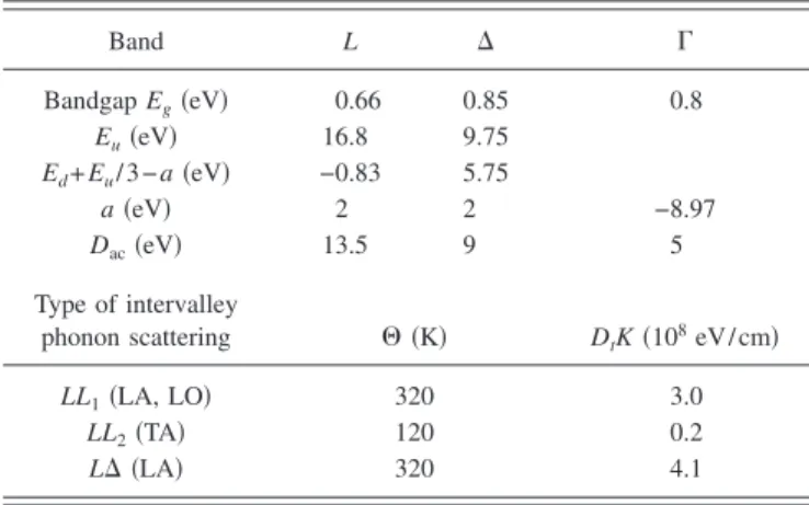
For strained Ge, given the stress magnitude and direc-tion, the strain tensor is obtained using a generalized Hooke’s law.9 The effect of substrate orientation is consid-ered by performing coordinate transformation. The strain-induced band-edge shifts are calculated using the linear deformation-potential theory with the parameters listed in Table I.10–12 The two-dimensional subband structure is ob-tained by solving the Poisson and Schrödinger equations self-consistently. The subband energy is a function of
un-strained band gap, strain-induced band-edge shift, and quan-tization splitting. The momentum relaxation rate is assumed to be isotropic using the relaxation time approximation. The anisotropy of the Ge band structure is retained, and the ef-fective masses are assumed to be unchanged under strain. The Kubo-Greenwood formula13is used to calculate the mo-bility for each subband. The scattering mechanisms take into account intravalley acoustic phonon scattering for each val-ley, L-L intervalley phonon scattering, L-⌬ intervalley pho-non scattering, and surface roughness scattering. The phopho-non scattering types and parameters are listed in TableIand are defined in Refs. 14 and 15. Autocorrelation function ⌬ = 0.4 nm and correlation length l = 1nm共Refs.16and17兲 are
used for surface roughness scattering; these are the values of Si, since values of Ge are not known, and a Si passivation layer is sometimes deposited on the Ge channel.18The total effective mobility is the population weighted average of all subband mobilities.
The highly anisotropic L valley results in unstrained mo-bility to be significantly dependent on substrate orientation,
a兲Author to whom correspondence should be addressed; electronic mail: [email protected]
FIG. 1.共Color online兲 Schematic diagram of the constant-energy contours in the conduction band for various substrate orientations. The inset shows the longitudinal and transverse effective masses of each band共Ref.8兲.
APPLIED PHYSICS LETTERS 91, 102103共2007兲
0003-6951/2007/91共10兲/102103/3/$23.00 91, 102103-1 © 2007 American Institute of Physics Downloaded 13 Feb 2009 to 140.112.113.225. Redistribution subject to AIP license or copyright; see http://apl.aip.org/apl/copyright.jsp
i.e., Ge共111兲⬎Ge共110兲关1¯10兴⬎Ge共001兲⬎Ge共110兲关001¯兴. 共 兲 and关 兴 are the notations of substrate orientation and channel direction, respectively. Regarding the in-plane mobility an-isotropy in unstrained channels, only共110兲 substrate shows anisotropy for different channel directions due to the twofold symmetry of the valley configuration共Fig.1兲. In the case of
unstrained共111兲 substrate, most electrons occupy the central L valleys 共Fig. 1兲 due to its relatively large quantization
mass, and the smallest conductivity effective mass of the central L valleys leads to the highest mobility.
In general, the mobility under uniaxial strain is channel-direction dependent. The channel channel-directions to achieve the highest mobility on共111兲, 共110兲, and 共001兲 substrates occur at关1¯10兴, 关1¯10兴, and 关110兴, respectively, with the tensile stress of 1 GPa 共⬃0.7% strain兲 parallel to the channel direction 共Fig.2兲.5The enhancement is mainly attributed to the reduc-tion of average conductivity mass caused by the electron repopulation from valleys with large conductivity mass to those with small conductivity mass. To ensure the validity of our approach, the calculated mobility of Si 共001兲 is com-pared with the published data19 共Fig. 2兲 and reasonable
agreement is achieved.
Figure3shows mobility as a function of biaxial strain on 共001兲 substrate. For strain smaller than 0.7% 共⬃1 GPa兲, L valleys dominate the mobility due to its occupancy exceed-ing 70%. Thus, the mobility under small biaxial strain is
similar to the unstrained case. In the case of the tensile strain larger than 2%共⬃2.8 GPa兲, the mobility increases rapidly. Significant occupancy in light-mass⌫ band for tensile strain larger than 2% is responsible for this共Fig.3兲. However, the
mobility enhancement for Ge channel on共001兲 substrate un-der large biaxial tensile strain is not as high as that in the bulk case, which has no quantum confinement and yields mobility over 10 000 cm2/ V s at 2% biaxial tensile strain.10 This is due to the quantum confinement at high vertical field, which leads to less occupancy of⌫ band in Ge channel than that of bulk Ge. On the other hand,⌬4valleys dominate the occupancy when compressive strain is larger than 1%, and the mobility is degraded due to the larger mass in⌬4valleys than that in L valleys.
Mobility as a function of strain for 共111兲关1¯10兴, 共110兲关1¯10兴, and 共001兲关110兴 at 1 MV/cm is shown in Fig.4. Note that biaxial strain is independent of the stress direction, while uniaxial tensile and compressive stress are applied par-allel and perpendicular to the channel direction, respectively, as shown in Fig.4. The perpendicular tensile strain has lower mobility than the parallel tensile strain, and the mobility un-der the parallel compressive strain is inferior to the perpen-dicular compressive strain. Therefore, these data are not shown in Fig.4. Under large strain, electrons are all popu-lated in the valleys with the lowest energy, and the average conductivity mass remains constant. Therefore, the mobility remains constant at large strain. Biaxial tensile strain and longitudinal tensile strain along the 关1¯10兴 channel direction TABLE I. Bandgap Eg, dilation deformation potentials Euand a, and shear
deformation potential Edfor L,⌬, and ⌫ bands. Also shown are the acoustic deformation potential Dacfor intervalley phonon scattering, and the defor-mation potential⌰ and DtK for intervalley phonon scattering.
Band L ⌬ ⌫ Bandgap Eg共eV兲 0.66 0.85 0.8 Eu共eV兲 16.8 9.75 Ed+ Eu/ 3 − a共eV兲 −0.83 5.75 a共eV兲 2 2 −8.97 Dac共eV兲 13.5 9 5 Type of intervalley
phonon scattering ⌰ 共K兲 DtK共108eV/ cm兲
LL1共LA, LO兲 320 3.0
LL2共TA兲 120 0.2
L⌬ 共LA兲 320 4.1
FIG. 2. 共Color online兲 Mobility as a function of effective vertical field for the uniaxial tensile stress of 1 GPa parallel to the channel direction on different substrate orientations. The mobility of unstrained Ge共111兲 channel and the Si universal mobility curve共Ref.19兲 are also shown for comparison.
FIG. 3. 共Color online兲 Mobility as a function of biaxial strain for 共001兲 substrate at Eeff= 1 MV/ cm. The inset shows the corresponding valley oc-cupation vs strain.
FIG. 4.共Color online兲 Mobility as a function of strain under different stress conditions, channel directions with notation of关 兴, and substrate orientations with notation of共 兲.
102103-2 Yang et al. Appl. Phys. Lett. 91, 102103共2007兲
give similar mobility enhancement on 共111兲 substrate. For 共111兲关1¯10兴, the highest mobility enhancement of 4.1 times of Si共001兲 universal mobility is achieved when tensile strain is larger than 0.5% 共⬃0.7 GPa兲. For transverse compressive strain larger than 1.5% 共⬃2.1 GPa兲, the mobility enhance-ment is found to be 2.9 times of Si共001兲 universal mobility. However, the mobility decreases very rapidly under biaxial compressive strain and falls below the Si universal mobility 共Fig.2兲 for 共110兲 and 共111兲 substrates. The band edges of L
valleys and ⌬ valleys become close under biaxial compres-sive strain, and the scattering rate increases accordingly. Both increases of conductivity effective mass and scattering rate account for the mobility degradation under compressive biaxial strain.
The strain effect on electron mobility of Ge n-MOSFETs is investigated. The共111兲 Ge FETs have the highest mobility among all three substrate orientations. The mobility enhance-ment can be found for all three substrate orientations if the channel direction and strain condition are optimized. The mobility optimization can facilitate the device design of Ge channel MOSFETs.
The National Taiwan University group is supported by National Science Council, Taiwan, under Contract No. NSC 95-2221-E-002-357. The grant from TSMC 共Taiwan Semi-conductor Manufacturing Company兲 is highly appreciated.
1C. C. Yeo, B. J. Cho, F. Gao, S. J. Lee, M. H. Lee, C.-Y. Yu, C. W. Liu, L. J. Tang, and T. W. Lee, IEEE Electron Device Lett. 26, 761共2005兲. 2M. L. Lee and E. A. Fitzgerald, Appl. Phys. Lett. 83, 4202共2003兲. 3S. Maikap, C.-Y. Yu, S.-R. Jan, M. H. Lee, and C. W. Liu, IEEE Electron
Device Lett. 25, 40共2004兲.
4S. Dhar, H. Kosina, V. Palankovski, S. E. Ungersboeck, and S. Selberherr, IEEE Trans. Electron Devices 52, 527共2005兲.
5H. Irie, K. Kita, K. Kyuno, and A. Toriumi, Tech. Dig. - Int. Electron Devices Meet. 2004, 225.
6K. Uchida, T. Krishnamohan, K. C. Saraswat, and Y. Nishi, Tech. Dig. -Int. Electron Devices Meet. 2005, 129.
7F. Stern and W. E. Howard, Phys. Rev. 163, 816共1967兲.
8A. Rahman, M. S. Lundstrom, and A. W. Ghosh, J. Appl. Phys. 97, 053702共2005兲.
9J. J. Wortman and R. A. Evans, J. Appl. Phys. 36, 153共1965兲. 10I. Balslev, Phys. Rev. 143, 636共1966兲.
11M. V. Fischetti and S. E. Laux, J. Appl. Phys. 80, 2234共1996兲. 12J. Liu, D. D. Cannon, K. Wada, Y. Ishikawa, D. T. Danielson, S.
Jongth-ammanurak, J. Michel, and L. C. Kimerling, Phys. Rev. B 70, 155309 共2004兲.
13R. Kotlyar, D. Giles, P. Matagne, B. Obradovic, L. Shifren, M. Stettler, and E. Wang, Tech. Dig. - Int. Electron Devices Meet. 2004, 391. 14S. Takagi, J. L. Hoyt, J. J. Welser, and J. F. Gibbons, J. Appl. Phys. 80,
1567共1996兲.
15C. Jacoboni and L. Reggiani, Rev. Mod. Phys. 55, 645共1983兲. 16T. Low, M. F. Li, C. Shen, Y.-C. Yeo, Y. T. Hou, and C. Zhu, Appl. Phys.
Lett. 85, 2402共2004兲.
17B. Ghosh, X. Wang, X.-F. Fan, L. F. Register, and S. K. Banerjee, IEEE Trans. Electron Devices 52, 547共2005兲.
18C.-Y. Peng, F. Yuan, C.-Y. Yu, P.-S. Kuo, M. H. Lee, S. Maikap, C.-H. Hsu, and C. W. Liu, Appl. Phys. Lett. 90, 012114共2007兲.
19S. Takagi, A. Toriumi, M. Iwase, and H. Tango, IEEE Trans. Electron Devices 41, 2357共1994兲.
102103-3 Yang et al. Appl. Phys. Lett. 91, 102103共2007兲