2004 IEEE Asia-Pacific Conference on Advanced System Integrated Circuits(AP-ASIC2004)/ Aug. 4-5,2004
15-5
A
1-4 GHz DLL
Based Low-Jitter Multi-Phase Clock Generator
for Low-Band Ultra-Wideband Application
Tsung-Te Liu and Chomg-Kuang Wang
Graduate Institute of Electronics Engineering, and Department of Electrical Engineering, National Taiwan University, 106 Taipei, Taiwan R. 0. C.
E-mail: ckwang@cc.ee.ntu.edu.tw
&ISTRACT or, equivalently, in terms of Tcw:
This paper presents the implementation of a low-jitter system clock generator for low-band ultra-wideband (UWB) application based on a wide-range adaptive-bandwidth delay-locked loop (DLL). The false-locking problem commonly along with the wide-range DLL is eliminated by the proposed digital self- correcting loop which also speeds up the lock-in time of the DLL. With self-biased techniques, the proposed DLL adaptively adjusts bandwidth and exhibits optimal jitter transfer characteristic over a wide frequency range and across process, voltage, and temperature (PVT) variations. Fabricated in a 0.18- pm CMOS technology, the design achieves an output multi- phase sampling clock rate of 1 to 4 GHz and exhibits the maximum input tracking jitter of 12.06 ps (m) and 88.9 ps (pk- pk) over the operating frequency range kom 31.25 to 125 MHz. The prototype occupies an active area of 360 x 245 pm' and consumes 32 mW from a 1.8-V supply at 125 MHz.
1. INTRODUCTION
The Federal Communications Commission (FCC) has opened the frequency bands for unlicensed ultra-widehand
(UWB)
wireless systems since February, 2002 [I]. System architectures for pulse-based UWB radio have been recently proposed targeting applications such as positioning system and sensor network. One critical aspect of VLSI implementation of pulse- based UWB radio is the accurate generation of timing signals to support reliable data communications [2].Phase-locked loops (PLLs) and delay-locked loops (DLLs) have been typically employed to generate high-frequency accurate system clock from a low-kequency, precise, and stable oscillator. Usually, DLLs are easier than PLLs to implement the clock generator. A DLL is unconditionally stable and only needs one capacitor
in
its fust-order loop filter, while a PLL generally requires a higher order filter which usually occupies large areas or needs to be off chip in order to guarantee the stability and performance. Moreover, a DLL offers hener jitter performancethan
a PLL because phase errors induced by supply or substrate noises do not accumulate over many cycles in the voltage- controlled delay line (VCDL) [3]. However, conventional DLLs may sutTer from false locking, which is undesirable if multi- phase clocks are needed. The maximum and the minimum delays of the VCDL, TvcDL.,, andTvcDL.,i,,
should satisfy the following inequalities to avoid a false locking [4]:0.5 X TCLK < TVCVL.,, < TCLK
TCLK
<TVCOL.-<
1.5 X TCLK (1)This work was supported in part by MediaTek Inc. Hsin Chu, Taiwan 300.
Max ( T V C D L . ~ U ~ 213 x T V C D L . ~ ) < TCLK
< Min ( 2 x T v c D L . ~ ~ ~ . TVCDL.,,
1
(2)where TcLK is the period of the input reference clock. If the target clock period.satisfies the inequality (2), the DLL works and does not posses a false-locking. However, if TvcDL., ? 3 x T v c o i . ~ , which is usually the case when process, voltage, and temperature (PVT) variations are taken into consideration, then there is no range of TcLK that satisfies the inequality (2). Therefore, the conventional DLL can only operate over a narrow frequency range if an exotic tedious trimming circuit for correct locking is not employed [4].
This paper proposes a novel DLL architecture without the false-locking problem which combines two techniques [SI, 161 for implementation of a low-jitter wide-range multi-phase clock generator. The output sampling clock rate of the proposed DLL spans from I GHz to 4 GHz, which is sufficient for low-band 960 MHz UWB system application [2].
The rest of this paper is organized as follows. Section 11 describes the proposed DLL architecture followed by the circuit design in Section 111. Experiment results are presented in Section IV. Section V concludes this paper.
11. DLL ARCHITECTURE
CK
.. ... ... . ...
.
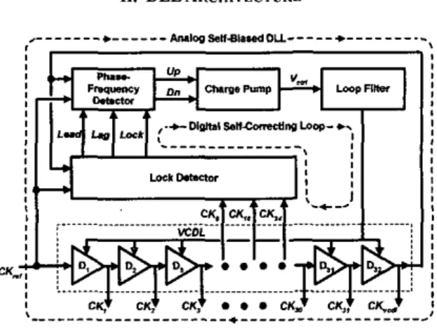
Fig. I Block diagram of the proposed DLL architecture.
Fig. 1 shows the architecture of the proposed low-jitter wide- range adaptive bandwidth DLL, which consists ofa main unalog se(f-biused DLL and an auxiliary digital sey-correcting loop. The phase-kequency detector (PFD), charge pump, loop filter, and 32-stage VCDL compose the DLL core. The self-biased circuits adjust the DLL Imp bandwidth adaptively. Therefore,
2004
IEEE
Asia-Pacific Conferenceon
AdvancedSystem
Integrated Circu~~(AF'-ASlC2OM)/ Aug. 4-5,2004the loop stability and an optimal jitter hansfer characteristic can be maintained over a wide frequency range and across PVT variations [6 ] . The auxiliary digital self-correcting loop consists of the same components of the DLL core except employing a lock detector to replace the PFD. It continuously monitors the DLL acquisition behavior and takes control of the loop if the phenomenon of false locking is detected. The lock detector utilizes three additional delayed clocks, CK,, CK,,, and CK, from VCDL to determine the preset lock-in state. It then generates three digital control signals, namely, Lead, Lug, and Lock. These digital control signals indicate whether the DLL is in false-locking state. That is, when the delay of the VCDL is too small, the Lead control signal is activated. The Lug control signal is activated to indicate the delay is too large. The lock detector can take over the loop from PFD and directly sense the charge pump to charge or discharge the loop through the Lead and the Lag control signals. On the other hand, if the delay of the VCDL is within the correct-locking range, the Lock control signal is activated and the DLL core restarts to acquire locking as usual. The auxiliary digital self-correcting loop extends correct-locking range of the DLL four times wider than that of the conventional design constrained by the inequality (I).
The critical path timing contributed by gate delays of the digital decision logics in the auxilialy digital self-correcting loop may he so large in high-speed operation that the switching from the auxilialy digital self-correcting loop to the DLL core cannot be accomplished in time. This might result in instability of the loop. The PFD is adopted to effectively increase switching timing margin and mitigate the problem of loop instability because it has a wider capture range of (-2
x
,+2x
) than the phase detector (PD) used in the previous architecture [ 5 ] .T m @SI
Fig. 2 Simulated loop acquisition behavior of the DLL (a) at 40 MHz and (b) at input clock frequency changed to 100 MHz afler 1.5 p.
Fig. 2 shows the simulated loop control voltage V , i and the Lock control signal when the DLL starts to acquire locking. In Fig. 2(a), the DLL starts at an input clock frequency 40MHz and the minimum VCDL delay. Once the lock detector detects the DLL core in false-locking state, it immediately disables the Lock control signal. Although the DLL core suffers 60m false locking, the loop can still lock to the right direction and exhibit slew behavior of maximum speed because of the operation of the auxiliary digital self-correcting loop. The Lock control signal is activated and the DLL core then regains control of the loop until the delay ofthe VCDL is within the correct-locking range. when the input clock frequency is suddenly changed to 100 MHz after 1.5 ps, where the conventional DLLs would suffer false-
locking problem, the proposed DLL can still react and operate properly, as shown in Fig. 2(h).
Ill. CIRCUITDESIGN A. Lock Detector ... L d L& L.p ;lnpufl.(rhuj j D T & c W C U ~ O ~ O L L I D ~ M ~ M . D ~ .
1
I ... 1 L ... , L d L& L.p ;lnpufl.(rhuj j D T & c W C U ~ O ~ O L L I D ~ M ~ M . D ~ .1
I ... 1 L ... ,Fig. 3 Schematic ofthe proposed lock detector.
(a) (b)
Fig. 4 Timing diagram ofthe DLL (a) with and (b) without guard latches included in the lock detector.
The schematic of the lock detector is shown in Fig. 3. The three delayed clocks from the VCDL, CK,, CK,,, and CKJI are first latched at the rising edge of the input reference clock
CK,<, The outputs of these latches are further processed to determine the present lock-in state by decode circuits. Two guard latches, which are trigged respectively by CK,,, and the delayed clock from the last stage of the VCDL, CKvcd,, are included in the decode circuits generating Lock control signal. Fig. 4 shows the detailed timing diagram of the DLL when the lock-in state of the DLL is changed from the Lag state to the
Lock
state. It illustrates the functionsof the
guard latches. The guard latches ensure the Lock control signal can be activated at the right momentso
that the PFD can generate proper control signals to keep the DLL core locking to the correct direction when it regains control of the loop from the reset state.B.
Dynamic-Switched Phase-Frequency DetectorFig. 5 shows the dynamic-switched PFD circuit, which consists of a dynamic logic PFD and digital control logics for lock detector. The Lead and Lag control signals
can
bypass the dynamic logic PFD to directly control the following charge- pump stage through these digital control logics. The logics included in the reset path properly reset the PFD when theLock
control signal is disabled. The exh'a gate delays in the reset path also help the PFD periodically produce a chain of short pulses in
2004
IEEE
Asia-Pacific Conference on Advanced System Integrated Circuits(AP-ASIC2004)/ Aug. 4-5,2004the locked state which can reduce the dead zone of the PFD effectively. The dynamic logic PFD is adopted here for the capability of higher speed operation in comparison with the static counterpart.
...
i ~ n u I 1 o * p F D ~
, ...
Fig. 5 Schematic of the dynamic-switched PFD circuit
C. Charge Pump and Voltage-Controlled Delay Line
Fig. 6 (a) Charge pump (b) delay cell of the VCDL with replica bias [ 6 ] .
The charge-pump circuit and the delay cell of the VCDL with replica bias are similar to those used in [6], as shown in Fig. 6. These circuits are biased with the VCDL control voltage, and their currents can he scaled with the operating frequency ofthe DLL consequently.
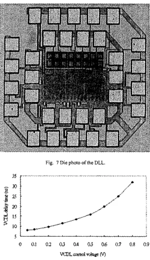
Fig. 7 Die photo of the DLL.
... ~
.
...i
4 0.1 0.2 03 0.4 0.5 06 0.7 0.R 0.9
WLccmtdV%arrN) Fig. 8 Measured transfer curve of the VCDL.
Fig. 9 DLL output jilter histogram at 125 MHz.
IV.
EXPERIMENTAL
RESULTSThe DLL has been designed and fabricated in a 0.18-@n ChlOS technology.
As
shown in the die photo in Fig. 7, the DLL core area is 0.09 nun' (360 @n x 245 pm). The experimental results show that the DLL can operate in the frequency range of 31.25 to 125MHz with a 1.8-V supply. Fig. 8 depicts the measured transfer curve of the VCDL. The tracking jitter2004
IEEE
Asia-Pacific Conferenceon
Advanced System
Integrated Circuits(AP-ASIC2004)/Aug.
4-5,2004Opcmting voltage Operating frequency range Output multi-phase dock rate
RMS jitter
Peak-to-peak jitter
Supply sensitivity Lock time Power dissipation
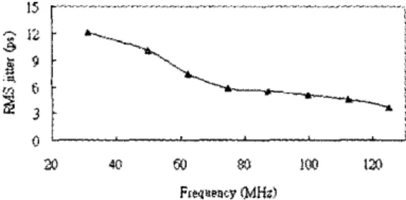
performance ofthe DLL output at 125MHz is demonstrated in Fig. 9. The jitter histogram measures 3.63-ps rms and 30.67-ps peak-to-peak jitter characteristics in a quiet supply. Fig. I O shows the measured rms jitter characteristics of the DLL over different operating frequencies. If a 100 mV Gaussian random noise is injected externally to the supply, the
rms
jitter and peak-to-peak jitter are increased to 12.23 ps and 90.7 ps respectively when the DLL operates at 125MHz, as demonstrated in Fig. 11. The equivalent jitter supply sensitivity is less than 0.91 pdmV. Table I summarizes the performance of the proposed DLL.~~ ~ 1.8V 31.25 MHz- 125 MHz I G H z - 4 G H z 12.06ps@3I.25 MHz 3.63 ps @ 125 M H z 88.9ps@31.25 MHz 30.67 ps @ 125 MHz < 0.91 psimV
~ 54 clock cycles (simulated)
32 mW @ 125 MHz
m
40 60 a3 1m 150Frequency (MHd
Fig. I O Measured ms jitter characteristics of the DLL over different operating frequencies.
Fig. I I DLL output jitter histogram at 125 MHz with LOO mV supply m i s e injected to the supply.
TABLE I
Performance summary of the pmpmed DLL
PrOCESS
I
0.18-pm lP6M TSMC CMOS processV. CONCLUSION
A self-hiased adaptive bandwidth DLL using an auxiliary digital self-correcting loop is proposed to achieve an optimal jitter transfer characteristic and avoid false-locking problem over a wide eequency range and across PV? variations. Compared with previous wide-range DLLs [4]-[8], the proposed DLL demonstrates smaller area cost, lower power consumption, and better jitter performance. The equivalent sampling clock rate of multi-phase clocks generated eom 32 taps of the VCDL can operate up to 4 GHz, which makes this DLL suitable for low- jitter clock generation in low-band UWB application.
ACKNOWLEDGEMENT
The authors would like to acknowledge Wei-Hsuan Tu, Hueng-lie Tsai, Chien-Cbih Lin and Prof. Shen-luan Liu for valuable technical discussions, Sung-Rung Han, Hsiang-Hui Chang, Rong-Jyi Yang and Chun-Pang Wu for testing support. They would further like to thank National Chip Implementation Center, Hsin Chu, Taiwan, for chip fabrication. This work was supported in part by MediaTek Inc. Hsin Chu, Taiwan 300.
REFERENCES
“Fint repon and o r d a in the matter of revision of P a l IS of the commission’s m l e ~ regarding Ultra-Wideband transmission rystans,” FCC, released. ET Dockel 98-153, FCC 0248, Apr. 22,2002. I. 0. Donnell, S. W. Chen, B. T Wan& and R. Brodnson. “An integrated IOW power ulm- wideband transceiver mhitechxe for low rate i n d w r wireless systems,” IEEE CAS Workhop on Wireless Communications andNeworking. Sep, 2002.
B. Kim, T. Weigands and P. Gray, “ P L I D L L system noise analysis for
low jitter clock rpthesirer d s i m , ” plot Int. S y q . Circuict ond Sysrem. Vol. 4, 1994, pp. 31-38.
Y. Mwn, J. Choi, K. Lee, D.-K Jeona and M.-K Kim, “An all-analog
multiohase delav-loek Iwo
~.
urine I a mlica.
delav line for wide-ranee Ioperation and low-jitter performance.” I E E E J Sold-State CirwiU, MI. 35, no.3,pp.377-3&2,Mar 2M)O.
D. J. Foley and M. P. Flynn, “CMOS DLL-based 2-V 3.2-ps jiller I. GHz clock s p t h s i a e r and temperahre-cornpensled tunable
oscillator,” IEEE J. Sold-St-srofe Circuits vol. 36, “0.3, pp. ~~ 417423, Mar. 2001.
J. Manpatis, “Low-jiuer pmeess-independent DLL and PLL based on sclf-biased techniques,” IEEE J. Sol;d-Srore Cimtlo, vol. 31, “0.1 I , pp. 1723-1732, Nov. 1996.
S. Sidimpoulos and M. A. Homwiu, “A semidigital dual delay-locked
Imp,”lEEEJ. Solid-Store Circuits, vol. 32, “0.1 I, pp. 1683-1692, Nov. 1997.
H. H. Chang, J. W. Lin, C. Y. Yang and S. 1. Liu, “A widerange delay locked loop with a fired latency of one clock cycle,”lEEEJ Solid-Store
Circuils. vol. 37,no.8,pp. 1021-1027, Aug. 1997.